
Wafer fab, process and packaging
From blank wafer to packaged die, explained step by step
Chartered Semi is a plain-language reference for chip design, wafer fabrication and advanced packaging, written for the people who work next to the process rather than around it.

Newest first
Latest explainers
The most recent guides published here, in the order they went up.
ESD Protection in Chip Design Explained: A Guide (2026)
ESD protection in chip design means building circuits on the die itself, at the I/O bond pads and supply rails, that shunt…
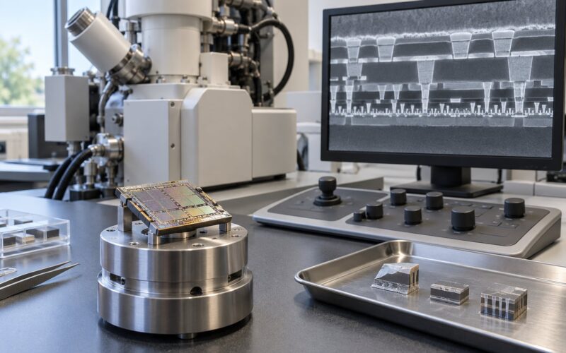
Scanning Electron Microscope for Semiconductor Failure Analysis 2026
Scanning electron microscope use in semiconductor failure analysis : how SEM reveals voids, cracks and delamination, and how to prepare and read…
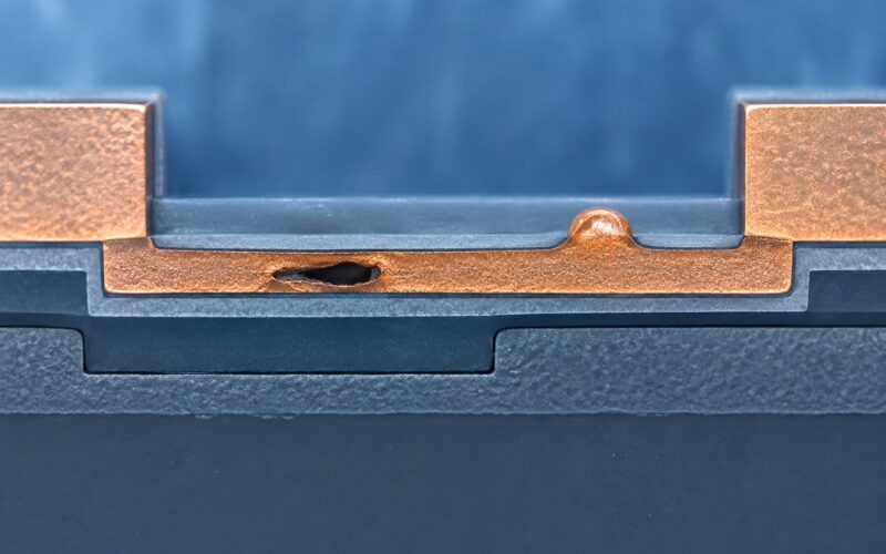
What Electromigration Is and Why It Kills Chips: A Guide 2026
What electromigration is and why it kills chips in : how current density, temperature, atom drift and rising resistance produce voids, opens…
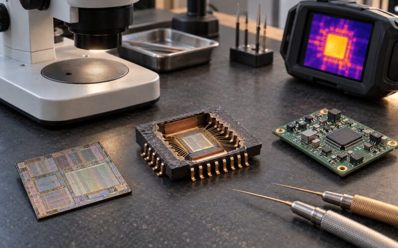
Failure Analysis Methods for Chips Explained (October 2026)
Failure analysis methods for chips explained step by step: electrical tests, X-ray and microscopy, fault localization, thermal imaging, chemistry, and root…
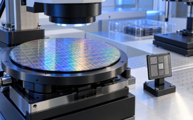
Metrology and Inspection in Chip Fabs Explained (2026)
Metrology and inspection in chip fabs explained : the tools, the process steps they watch, how defects are caught, and how the…
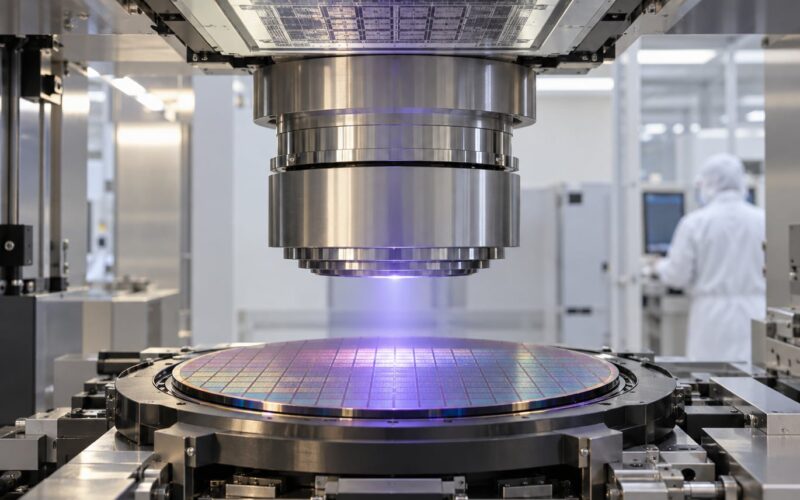
Reticle and Stepper Basics Explained Simply for Chipmakers 2026
Reticle and stepper basics explained through a clear chipmaking workflow, from photomasks and UV light to alignment, resolution, defects, and inspection.
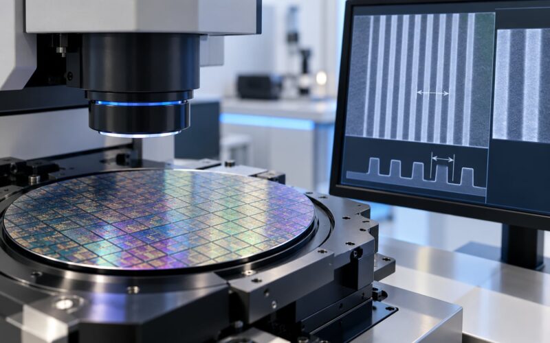
Critical Dimension Measurement Explained for IC Fabs (October 2026)
Critical dimension measurement explained for IC fabs: how CD metrology works, the main methods, uncertainty budgets, sampling and process control in .
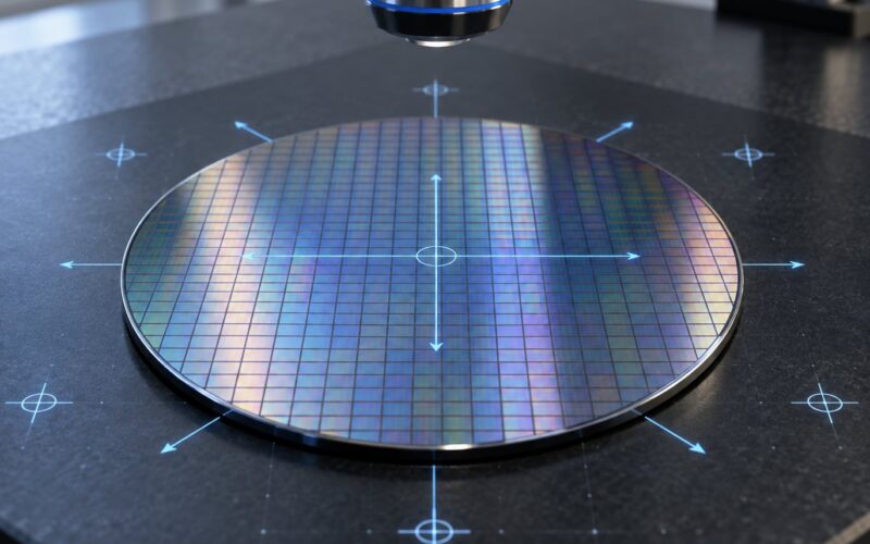
What Overlay Error Means in Lithography: Causes and Fixes 2026
What overlay error means in lithography: X/Y offsets, target marks, vector maps, causes, correction loops, node tolerances, and troubleshooting, updated for…
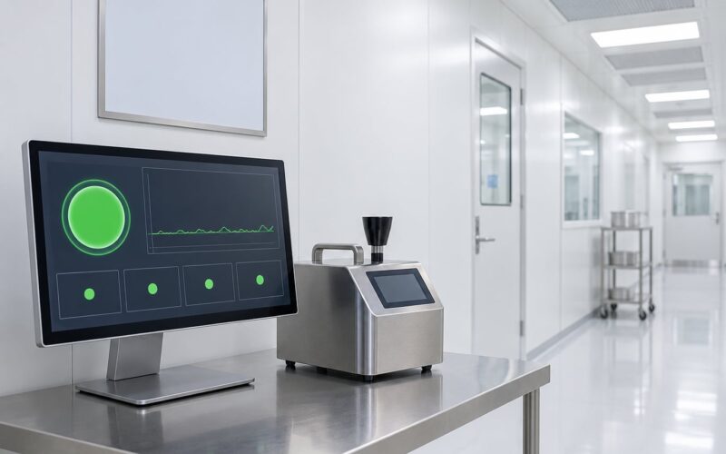
Cleanroom Class Ratings Explained for Semiconductor 2026
Cleanroom class ratings explained for semiconductor pros: ISO 1 to ISO 9 particle limits, fab applications, legacy Class 100 labels and how…
The process stack
Browse by topic
Every guide is filed under the part of the flow it belongs to, from design through fab to assembly and test.
Asked at the design review
Questions this site answers
- What actually happens during a single lithography step?
- Why can a design that passes timing still fail in silicon?
- When does advanced packaging beat moving to a smaller node?
- Which process choices drive the cost of a wafer the most?
What this site is for
A reference for how chips get made
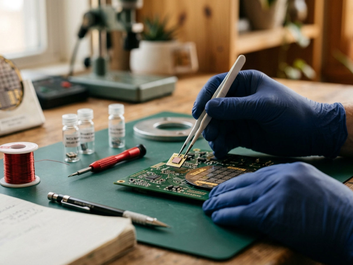
Chartered Semi explains how a chip goes from design intent and mask data through lithography, etch and deposition to assembly, packaging and test, one step at a time and without the marketing layer.
It is written for fabless engineers, EDA and IP users, students reading their way into the industry, and anyone who needs the process described in terms they can use.