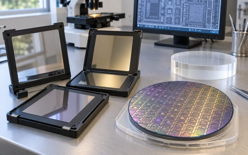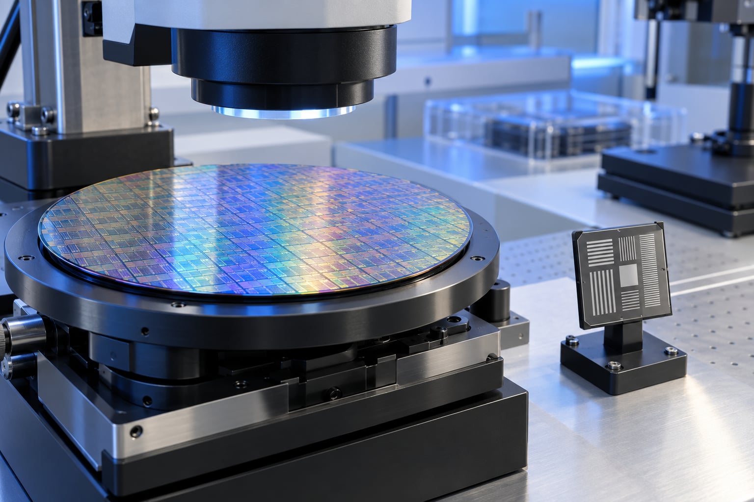
Metrology and inspection in chip fabs explained starts with one simple split: metrology measures a known process parameter, and inspection looks for something that has gone wrong. A fab runs both, repeatedly, across a 400-to-600-step wafer cycle that can take one to two months from start to finish. Without those measurements, a single stray particle or a 2 nm drift in a line width gets copied onto every die on the wafer and then into every wafer behind it.
This guide walks the whole thing in order: what each discipline does, where they sit in the flow, which tools do the work, how engineers measure the parameters that matter, and what happens the moment a defect shows up. It is written for process engineers, fabless designers, packaging engineers, students and business analysts who need a working mental model rather than a vendor pitch.
Table of Contents
- What Is Metrology and Inspection in Chip Fabs?
- Why Metrology and Inspection Matter in Semiconductor Manufacturing
- Yield and defect containment
- Process stability across hundreds of steps
- Customer qualification and reliability
- Wafer cost and throughput
- How the Semiconductor Manufacturing Process Uses These Tools
- 1. Incoming wafer qualification
- 2. Lithography and pattern transfer
- 3. Etch, deposition and ion implantation
- 4. Chemical mechanical planarisation and cleaning
- 5. Back-end metallisation and assembly
- 6. Final test
- The Main Metrology and Inspection Methods in Chip Fabs
- Key Tools Used in Chip Fabs
- How Fab Engineers Measure Critical Process Parameters
- What Happens When a Defect Is Found?
- How Data from Inspection Becomes Process Control
- Statistical process control answers: is this normal?
- Run-to-run control and APC answer: what should I change?
- Fault detection and classification answers: what is the tool doing?
- Virtual metrology answers: can we skip the measurement?
- Metrology and Inspection Limits and Common Challenges
- Frequently Asked Questions
- What is the difference between metrology and inspection in a chip fab?
- Which semiconductor process steps rely most heavily on metrology?
- What is CD-SEM and what does it measure?
- How do fabs detect microscopic defects without stopping every wafer?
- Why are sampling and statistical process control important in semiconductor inspection?
- Does more inspection always improve semiconductor yield?
- Conclusion: Where to Start If You Are New to This
What Is Metrology and Inspection in Chip Fabs?
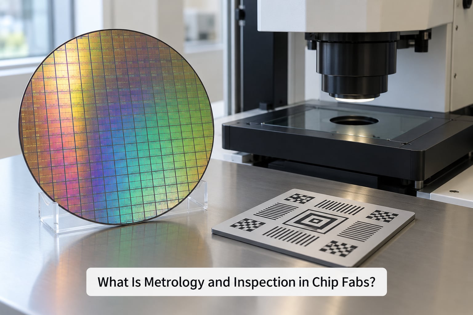
Metrology is the science of measuring a specific, known property of a wafer or device: line width, layer-to-layer registration, film thickness, dopant concentration, sheet resistance. Inspection answers a different question: is there anything on this wafer that should not be there — a particle, a bridge, a broken line, a void inside a package?
That contrast is the single most useful thing to carry out of this article. Metrology asks “how big is it and is it in spec?” Inspection asks “what is there and how bad is it?” Fabs need both, because a process can sit perfectly on target while still producing a defective die, and a die can be clean while the process behind it has drifted off target.
Inline process monitoring is the third thing that gets confused with the other two. Inline tools sit inside the process flow, right after the step that made the feature, so an engineer learns about a problem while the wafer is still early in its cycle. Final electrical test happens weeks later, after packaging, when a bad die can only be binned out rather than prevented. Metrology and inspection in chip fabs sit mostly in the first category: catching problems early enough to fix them.
For scale, one of the structures on an advanced logic wafer is around 1 nm wide. Human hair is 60 to 100 micrometres across, a typical bacterium is about 1 micrometre, and particles in cigarette smoke are roughly 100 nm. The measurement problem is not “can we see it,” it is “can we see it, measure it correctly, and do it fast enough not to slow the line down.”
Why Metrology and Inspection Matter in Semiconductor Manufacturing
Every measurement in a fab exists to stop one of three things: escaped defects, drifting processes, or wasted process time. The economics are severe because a defect caught at step 12 costs a wafer; the same defect caught at step 400 costs twelve months of engineering time.
Yield and defect containment
Yield is simply the number of working dies divided by all dies. Yield loss from random particles scales with process steps, so a 400-step flow punishes any contamination event far harder than a 50-step flow. Inline defect inspection builds a defect map across the wafer, which tells an engineer whether the particles sit on the wafer edge, in a ring pattern, or clustered near a specific tool chamber. That pattern is usually the whole investigation.
Process stability across hundreds of steps
Each tool drifts slightly with every wafer it processes. Nobody runs 400 steps perfectly; a fab runs 400 steps inside a narrow enough window that the finished chip still meets its electrical specification. Metrology is how that window is tracked, and statistical process control (SPC) is the method used to know whether a drift has become a trend.
Customer qualification and reliability
Automotive, aerospace and medical customers qualify a process, not a tool. Qualification packages are built from measurement data showing that a device meets its specification across temperature, voltage and time corners, with margin. A fab that cannot produce repeatable measurements cannot defend that margin to an auditor.
Wafer cost and throughput
Metrology and inspection equipment is a meaningful share of a fab’s capital spending, and every second a tool spends measuring is a second it is not processing. Insufficient inspection raises yield loss; excessive inspection raises cost and cycle time. Most of the engineering judgement in this field sits in that trade-off.
How the Semiconductor Manufacturing Process Uses These Tools
A modern flow is usually grouped into four stages: wafer preparation, front-end-of-line (FEOL, where the transistor is built), back-end-of-line (BEOL, where the metal interconnect is built), and assembly and test. Each stage has its own measurement signature. A new device in development can pass through several thousand individual metrology operations before it is qualified.
1. Incoming wafer qualification
Before processing, bare silicon wafers are checked for bow, warp, thickness variation, surface particles, crystal defects and, for advanced nodes, the defect maps that predict where random defects will appear. Surface particle levels here set the baseline for everything that follows.
2. Lithography and pattern transfer
Lithography is the most metrology-dense step in the entire fab. Overlay (layer-to-layer alignment), critical dimension (the width of a printed line), sidewall angle, pitch and printability are measured on dedicated tools, plus reticle qualification on the mask side. Every EUV or deep-ultraviolet layer repeats this pattern.
3. Etch, deposition and ion implantation
After pattern transfer, optical metrology checks film thickness and composition after every deposition or etch step, and electrical checks such as four-point probe sheet resistance verify that implant and anneal doses landed correctly. Depth profiles from secondary ion mass spectrometry (SIMS) are used during development, where speed matters less than understanding.
4. Chemical mechanical planarisation and cleaning
After each polish step, the wafer is measured for remaining metal, dishing and erosion. Cleaning steps are verified by particle counts, because a clean process is judged as much by what it did not add as by what it removed.
5. Back-end metallisation and assembly
BEOL adds the densest metrology burden in the process. Low-k dielectrics, copper or cobalt lines, and multi-layer stacks are measured for thickness, composition and critical dimension. In advanced packaging, through-silicon vias (TSV), hybrid bonding and high-bandwidth memory (HBM) stacks bring their own metrology discipline: X-ray and computed tomography for buried voids, acoustic inspection for delamination, and overlay measurement on the bond interface.
6. Final test
Wafer sort and final test apply electrical test: probe cards contact pads, parameters are measured, and dies are binned. This is the last line of defence, and unlike inline metrology it tells you the truth about the device rather than about the process.
The Main Metrology and Inspection Methods in Chip Fabs
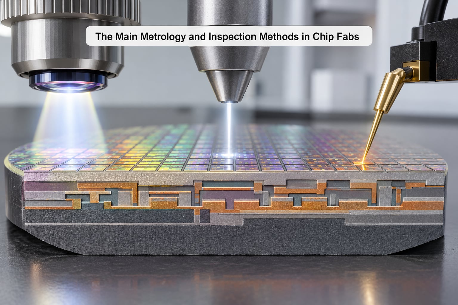
Five measurement families cover nearly everything a fab does. Optical methods are fast and non-destructive, so they carry the volume of routine production measurement. Electron-beam methods are slower but see far smaller features, so they are used for critical dimension and for high-sensitivity defect review. Electrical methods measure what the device actually does. Physical and materials methods explain why.
| Method | What it measures | Typical technique |
|---|---|---|
| Dimensional (CD) | Line width, hole diameter, sidewall angle, pitch | CD-SEM, optical critical dimension (scatterometry), AFM |
| Optical | Film thickness, composition, overlay, topography | Ellipsometry, reflectometry, X-ray reflectometry (XRR), X-ray fluorescence (XRF), overlay tools |
| Electron beam | Fine pattern defects, buried features, high-resolution CD | Scanning electron microscopy (SEM), e-beam defect inspection and review |
| Electrical | Sheet resistance, dopant profile, leakage, timing, capacitance | Four-point probe, SIMS, wafer sort and final test |
| Physical and materials | Surface chemistry, stress, defects inside a stack | X-ray photoelectron spectroscopy (XPS), AFM, X-ray and CT, acoustic inspection |
Inspection is then organised by what it looks at and by the physics it uses. Brightfield and darkfield optical systems trade sensitivity against throughput; electron-beam inspection finds smaller defects but is far slower; X-ray and CT see inside a package without opening it.
| Inspection target | Imaging physics | What it is used for |
|---|---|---|
| Bare wafer surface | Brightfield, darkfield, scatterometry | Incoming particle counts, surface defect maps, bow and warp |
| Patterned wafer | Brightfield, darkfield, e-beam | Line break, bridge, residual pattern, defect density monitoring |
| Mask or reticle | Optical, actinic, e-beam | Absorber defects, phase defects, pattern fidelity before printing |
| Package or advanced stack | X-ray, CT, acoustic, optical | Voiding, delamination, bump and TSV integrity, wire bond quality |
Key Tools Used in Chip Fabs
Eight tool families cover most of what a fab measures. CD-SEM is the workhorse for line width and hole diameter; it scans an electron beam across a pattern and measures from the image. Overlay metrology compares two printed layers to compute misregistration, usually in nanometres, and it is the tool that tells a lithographer whether the scanner is holding alignment. Defect inspection systems sweep a wafer with optical or electron-beam optics and build a defect map with coordinates and severities.
Film and profile tools cover thickness and composition. Ellipsometry and X-ray reflectometry measure dielectric and metal films fast enough for production; reflectometry and profilometry handle thicker films and step heights. Mask metrology tools, frequently supplied by the lithography vendor, check reticles with actinic light or electron beams, since a printing mask defect repeats on every die on every wafer it touches. Electrical test systems, from four-point probe to high-speed parametric test, measure resistance and device parameters. Process-control software sits on top of all of it, turning raw readings into control limits and recipe changes.
Not every technique exists in every production fab. Practitioners on r/Semiconductors make this point often: X-ray photoelectron spectroscopy is frequently a development or lab capability rather than a high-volume production tool, and whether a fab runs atomic force microscopy depends on the company and the product. Treat any vendor claim that one method covers everything with a grain of salt.
Two vendors dominate defect inspection, and practitioners ask for a neutral view of that rather than marketing. KLA Corporation is the reference name in optical and e-beam inspection; Applied Materials, Onto Innovation, Hitachi High-Tech, Camtek, Nova and Zeiss supply meaningful shares across optical, e-beam, metrology and mask inspection. The practical difference between them usually shows up in sensitivity per wafer-hour on a specific layer, not in a feature list.
How Fab Engineers Measure Critical Process Parameters
Eight parameters get measured again and again. Engineers care less about a single number than about whether a number is trending toward a limit, because a process that is drifting is a process that will eventually fail.
| Parameter | Primary tool | How it is sampled |
|---|---|---|
| Line width (critical dimension) | CD-SEM, optical critical dimension | 10 to 100 points per die, a handful of dies per wafer |
| Overlay | Overlay metrology, dedicated and lithography-integrated | Sampled per lot and per field across the wafer |
| Film thickness | Ellipsometry, XRR, reflectometry | Fixed points across the wafer, sometimes full-wafer maps |
| Composition and dopants | XPS, SIMS, XRF | Mostly during development; spot checks in production |
| Topography and profile | AFM, profilometry, SEM cross-section | Infrequent, targeted sites |
| Defects | Brightfield, darkfield, e-beam inspection | Full wafer sweep, sampled fields on large die |
| Electrical parameters | Four-point probe, parametric test, wafer sort | Structures per wafer plus every die at test |
| Process signatures | FDC sensor data, combined with SPC | Every wafer, every chamber |
The sampling numbers matter more than they look. A representative production strategy measures on the order of 10 to 100 points within a die, across 5 to 20 dies on a wafer, on 1 to 2 wafers out of a 25-wafer lot. Nobody measures every point on every die, because the time cost would be impossible and most of the wafer is identical anyway.
What Happens When a Defect Is Found?
The response runs in a fixed order, and engineers describe it roughly the same way regardless of the company. First the defect is detected and its coordinates recorded on a defect map. Then it is reviewed, either automatically or on a review tool that images the site again at higher resolution to separate a real defect from a nuisance signal. Then it is classified by type and size, and the class counts across the lot produce a Pareto picture of what kind of defect dominates.
Next comes root cause. A defect cluster that follows a specific tool chamber, a specific handler, or a specific edge location points to equipment. A cluster that follows a specific wafer position points to a process or handling issue. At this stage the lot is usually held, because a lot on hold means the remaining wafers stay at the fab instead of shipping to a customer.
Then the process is adjusted. Depending on the layer, that might be a lithography dose and focus correction, an etch time or endpoint change, a deposition rate trim, or a clean chamber service. Finally somebody decides disposition: release the held lots if the excursion was contained and electrical test supports it, rework if the failure mode is recoverable, or scrap if it is not.
That last decision is the expensive one. Scrap is simple and unambiguous, but it wastes the whole cycle. Releasing early and shipping a marginal lot risks a field failure months later. Most fabs lean conservative, because a customer return costs far more than a few wafers.
How Data from Inspection Becomes Process Control
Raw measurement data is close to useless on its own. It becomes useful when it passes through four layers, and each layer answers a different question about the process.
Statistical process control answers: is this normal?
SPC plots each measurement against control limits derived from the process history. A point inside the limits is expected behaviour; a point outside them is a signal. This is the simplest and most important layer, and it is also where most engineers on forums say they learned to read a process.
Run-to-run control and APC answer: what should I change?
Run-to-run (R2R) control adjusts a recipe before the next wafer, using the measured output of the previous one. Automated process control (APC) is the fuller version: a model that uses multiple measurements and, where appropriate, fault data to set several tool parameters at once. Both exist to keep a slow drift from becoming an excursion.
Fault detection and classification answers: what is the tool doing?
Fault detection and classification (FDC) watches sensor streams on the tool itself — pressures, temperatures, RF power, motor positions — and labels the many normal behaviours that would otherwise look like anomalies. It separates a real excursion from the ordinary cycle-to-cycle variation of a chamber.
Virtual metrology answers: can we skip the measurement?
Virtual metrology predicts the measurement result from FDC data instead of taking it. It exists purely for throughput: if the prediction is trusted, the tool can skip the physical measurement, and the wafer keeps moving. It is used selectively, on steps where the physical metrology step is the throughput bottleneck.
The loop closes when the lot disposition feeds back into the limits and models that produced the alarm. That feedback is why process control gets better over time rather than simply repeating the same decisions.
Metrology and Inspection Limits and Common Challenges
Five limits shape every decision in this field, and they are worth naming plainly rather than leaving to a vendor’s advantage.
Sampling is the first. Metrology is never 100 percent coverage, because measuring everything on every wafer at every step is economically impossible. That means rare defect populations can hide between sampled sites, and fabs manage the risk with defect detection tools, which do sweep whole wafers even when dimensional metrology does not.
Resolution and sensitivity are the second. Each tool has a defect size it reliably catches, and the industry keeps pushing that number down as features shrink. Brightfield and darkfield optical systems dominate because they are fast; electron-beam systems see smaller defects but trade throughput for it.
Measurement uncertainty is the third, and it is the one that bites hardest at advanced nodes. A process window of a couple of nanometres is being compared against an uncertainty budget that includes tool matching across a fleet, reference standard drift and sampling error. Gauge repeatability and reproducibility (gauge R&R) work exists to quantify that, and a fab that skips it is partly guessing. High-NA extreme ultraviolet (EUV) lithography widens the same gap, because resolution gains arrive with new metrology demands.
False positives are the fourth. Every nuisance signal an inspection tool reports costs review time, and review time costs throughput. Reducing the false-positive rate is one of the clearest genuine wins available to machine learning today: classifying real defects away from noise is a bounded problem with a measurable payoff. Claims beyond defect classification deserve scepticism.
Tool matching and cost are the fifth. A fab that owns 40 copies of the same metrology tool needs all 40 to read the same, or the SPC data becomes meaningless. Matching a fleet, calibrating against reference standards and retiring an outlier tool are real, unglamorous work. Advanced packaging and HBM add a further layer, because stacked die and fine-pitch bonding create defect types that front-end optical and e-beam tools were never designed to see.
Frequently Asked Questions
What is the difference between metrology and inspection in a chip fab?
Metrology measures a known process parameter such as line width, film thickness, overlay or sheet resistance and answers whether it is in specification. Inspection looks for what should not be there, including particles, bridges, broken lines and voids, and produces a defect map with locations and severities. Fabs need both: a process can sit on target and still produce a defective die.
Which semiconductor process steps rely most heavily on metrology?
Lithography is the most measurement-dense step, with dedicated checks on overlay, critical dimension, sidewall angle and printability at every layer. Deposition and etch follow closely, each verified for film thickness and composition. Planarisation and cleaning are checked for residual material and particle counts. Advanced packaging is emerging as a heavy user because stacked die and TSV structures hide defects from optical tools.
What is CD-SEM and what does it measure?
CD-SEM is a critical-dimension scanning electron microscope. It scans a focused electron beam across a pattern on a wafer and builds a high-resolution image from the reflected electrons, then measures line width, hole diameter and sidewall angle from that image. It is slow compared with optical methods, so fabs sample it at points within a die and on a handful of dies per wafer.
How do fabs detect microscopic defects without stopping every wafer?
Inspection systems do sweep whole wafers, so defects are found without stopping production, but they do not stop the flow to report every finding. Real-time signals are streamed to a defect map and triaged automatically; only the worst sites are re-imaged on a slower review tool. That triage is what keeps throughput viable, and machine learning is used mainly to cut the false positives that would otherwise fill the review queue.
Why are sampling and statistical process control important in semiconductor inspection?
Measuring every site on every wafer at every step is economically impossible, so fabs sample and rely on statistics to infer the rest. A common strategy takes on the order of 10 to 100 points within a die, across 5 to 20 dies per wafer, on 1 to 2 wafers of a 25-wafer lot. SPC turns those points into control limits so a genuine drift is separated from ordinary variation.
Does more inspection always improve semiconductor yield?
No. Every inspection step adds cost, cycle time and equipment capacity, and a badly tuned system spends most of that budget on false positives that waste review time. Extra inspection pays off where it targets a defect mode you can actually observe, at a sensitivity that matches the feature size. Excessive or low-yield inspection is overhead, which is why sampling and defect pareto analysis drive the schedule.
Conclusion: Where to Start If You Are New to This
Start with the distinction. Metrology answers how big and in spec; inspection answers what is there and how bad. Everything else in a fab’s measurement organisation follows from that split, including which tool gets bought and where it sits in the flow.
Second, learn one flow end to end. Pick a wafer, walk it from incoming check through lithography, etch, deposition, planarisation, packaging and final test, and write down the measurement made at each step. That single exercise explains sampling, SPC and excursion response better than any definition list.
Third, get comfortable with the numbers. Ten to 100 points per die, 5 to 20 dies per wafer, 1 to 2 wafers per 25-wafer lot, a 400-to-600 step cycle running one to two months, features around a nanometre wide. Metrology and inspection in chip fabs only make sense once those magnitudes are anchored, because every tool choice and every sampling decision is a trade between those scales and your cycle time.