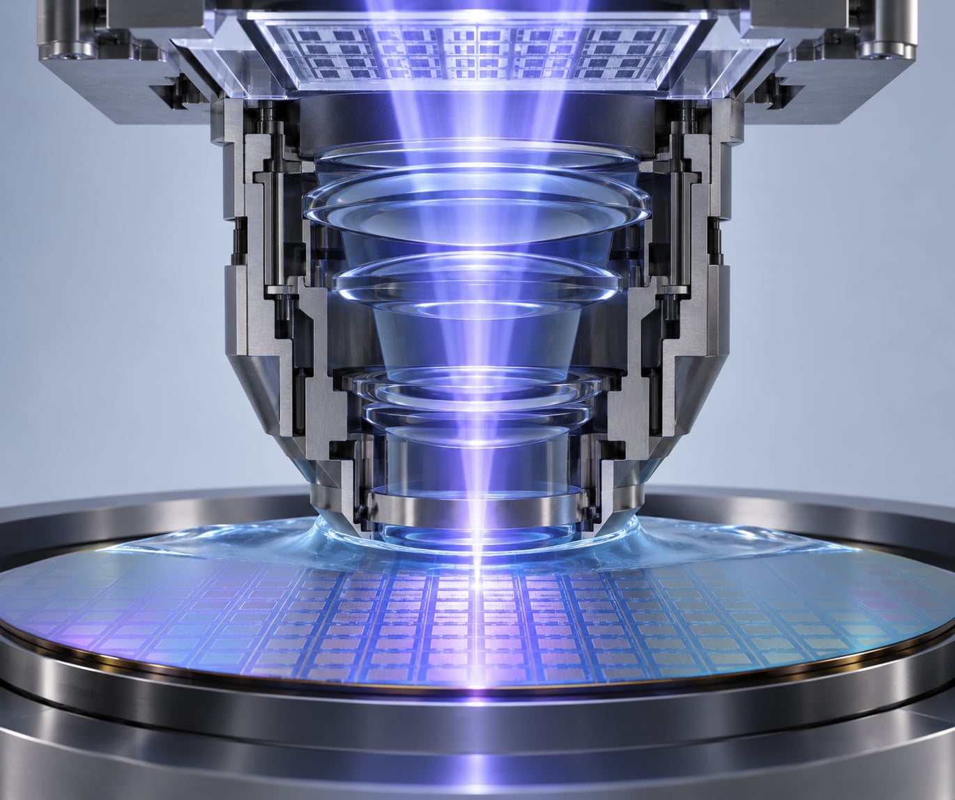
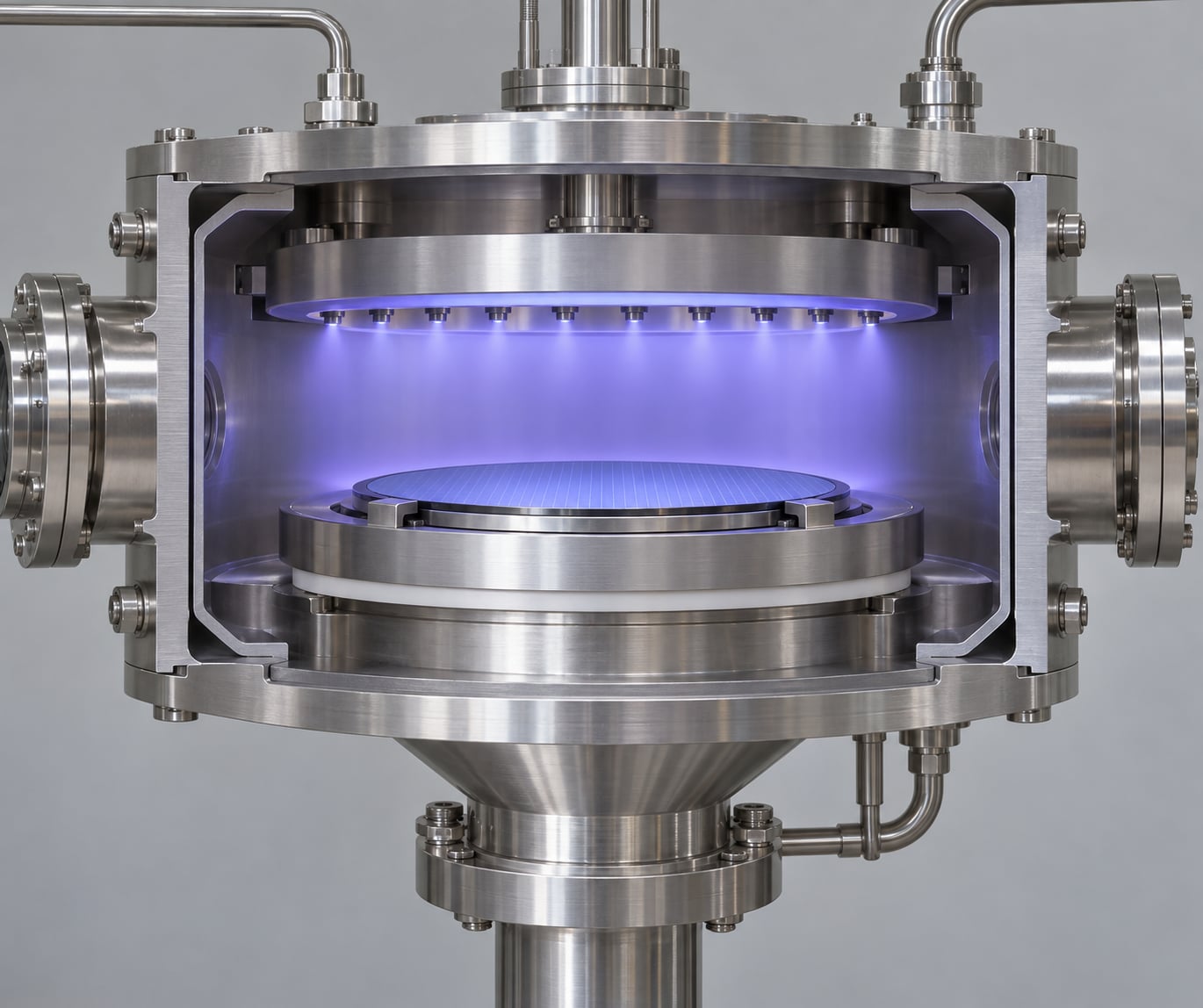
Scanning Electron Microscope for Semiconductor Failure Analysis 2026
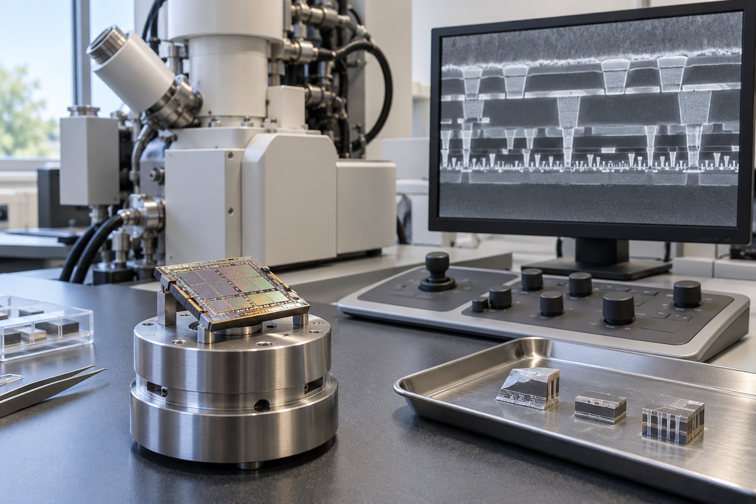
Scanning electron microscope use in semiconductor failure analysis is about looking where the fault is hidden. When a part fails electrically, the SEM gives … Read more
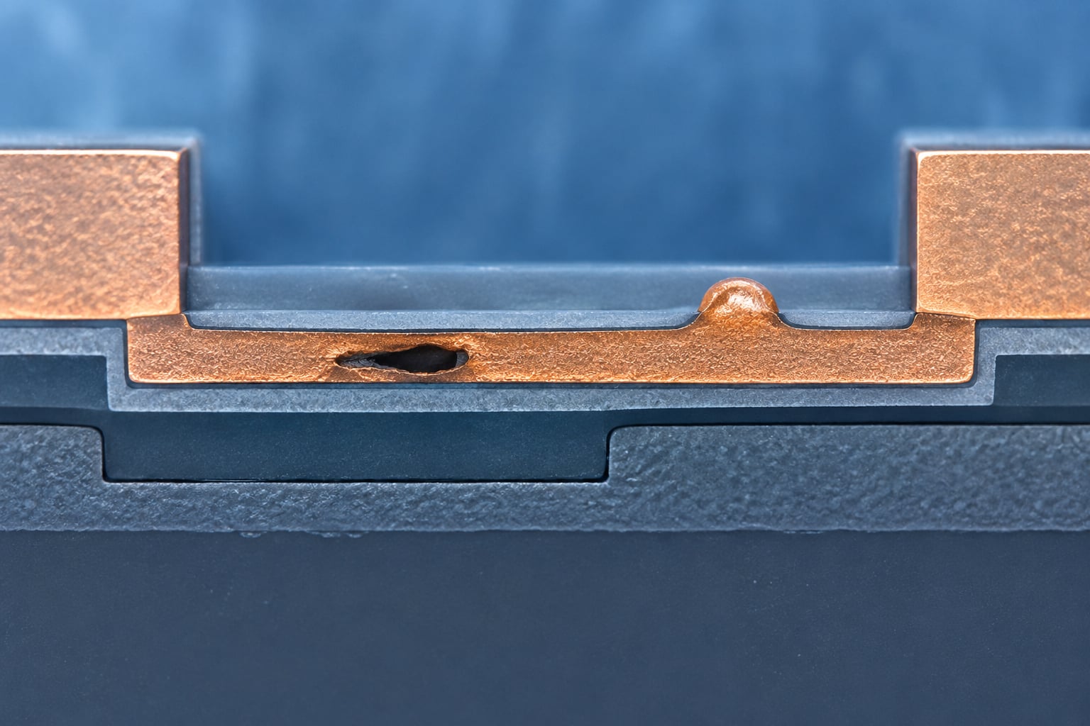
Electromigration is the slow, permanent movement of metal atoms inside a conductor, driven by momentum transfer from electrons that are flowing through it. Inside … Read more
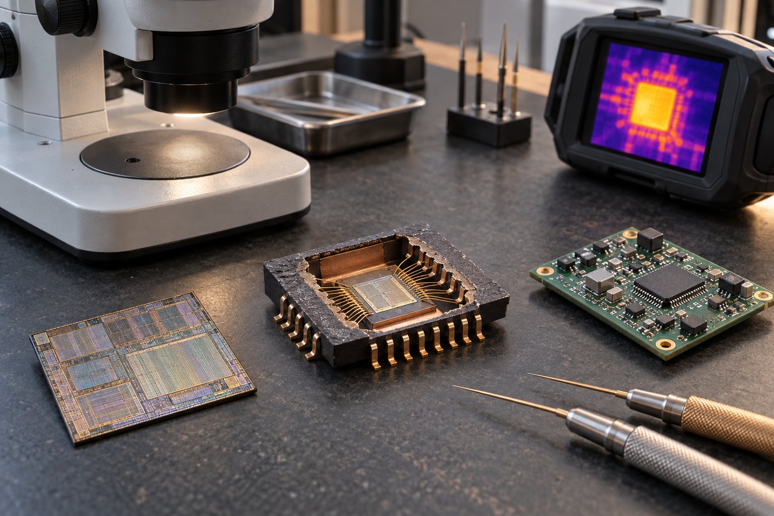
Semiconductor failure analysis is the systematic investigation of why an integrated circuit, its package, or the board around it stopped meeting specification. Failure analysis … Read more
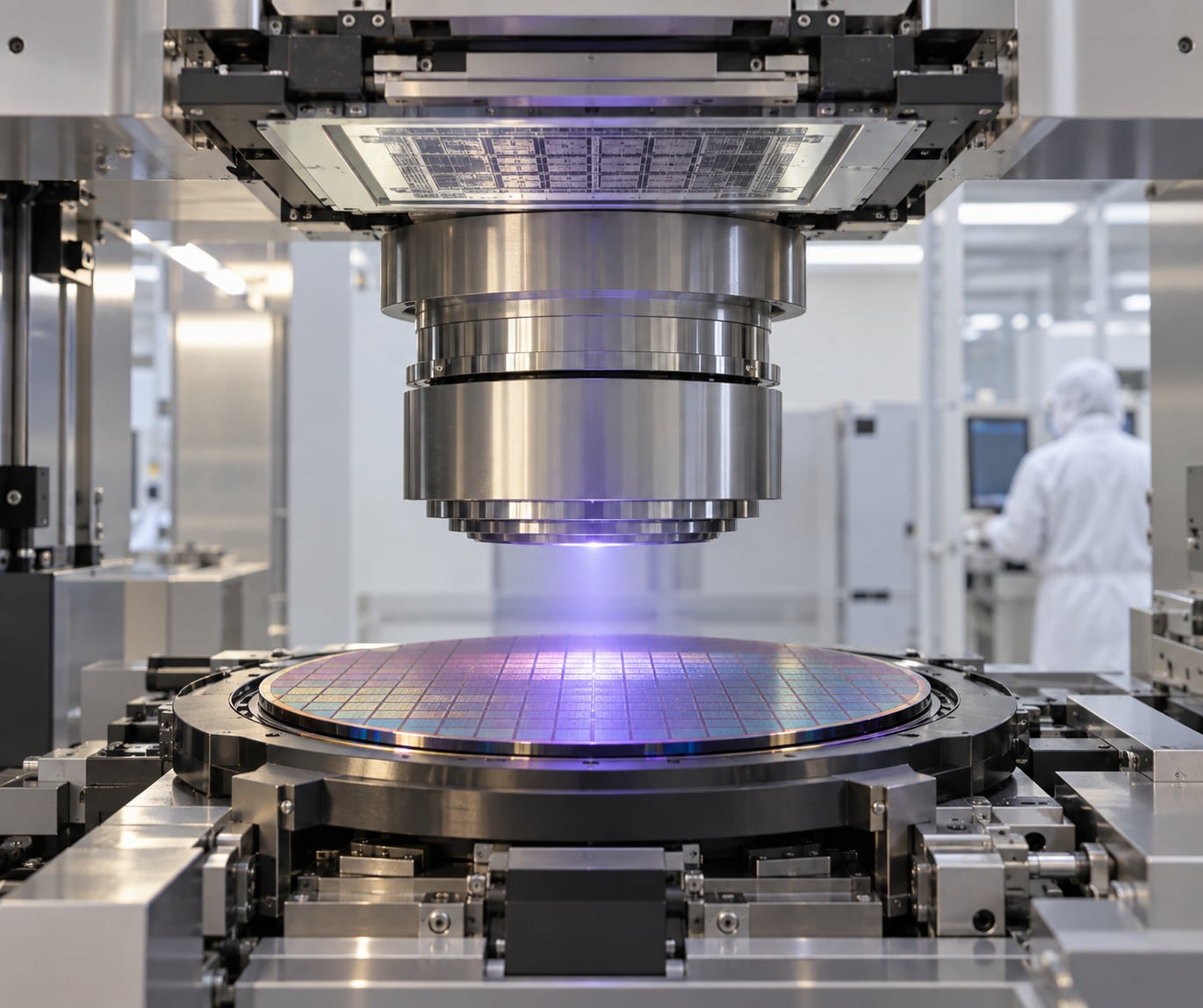
A reticle is the patterned glass plate that holds a chip’s circuit layout, and a stepper is the machine that repeatedly prints that layout … Read more
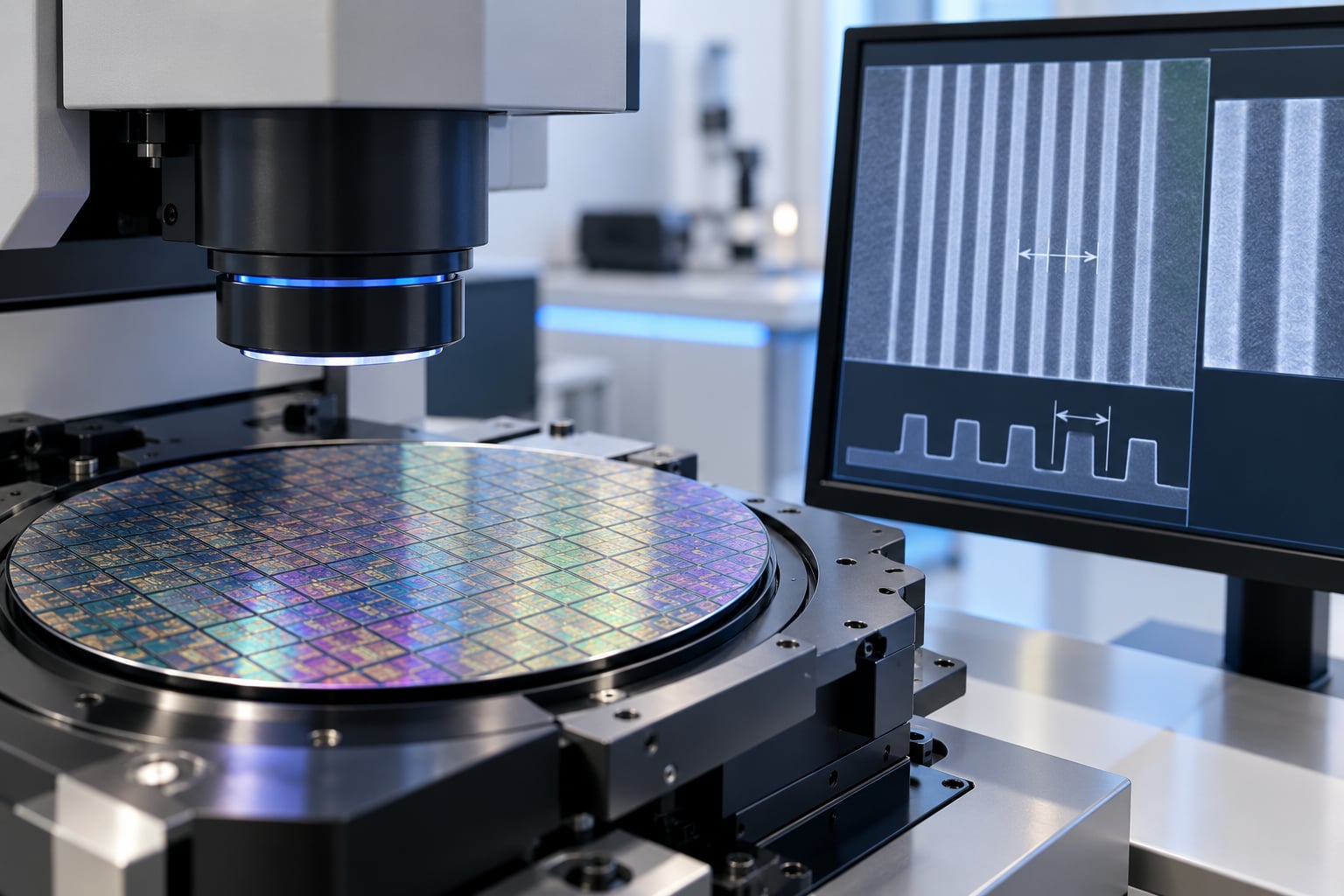
Critical dimension measurement is how a fab measures the width, height or sidewall profile of a printed feature so it can hold it inside … Read more
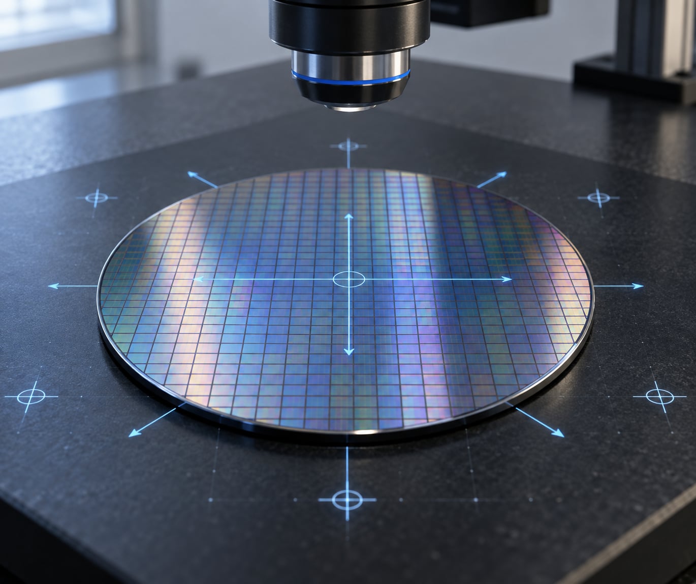
Overlay error is the unwanted positional difference between a lithographic layer and the layer it is supposed to sit on top of. It is … Read more
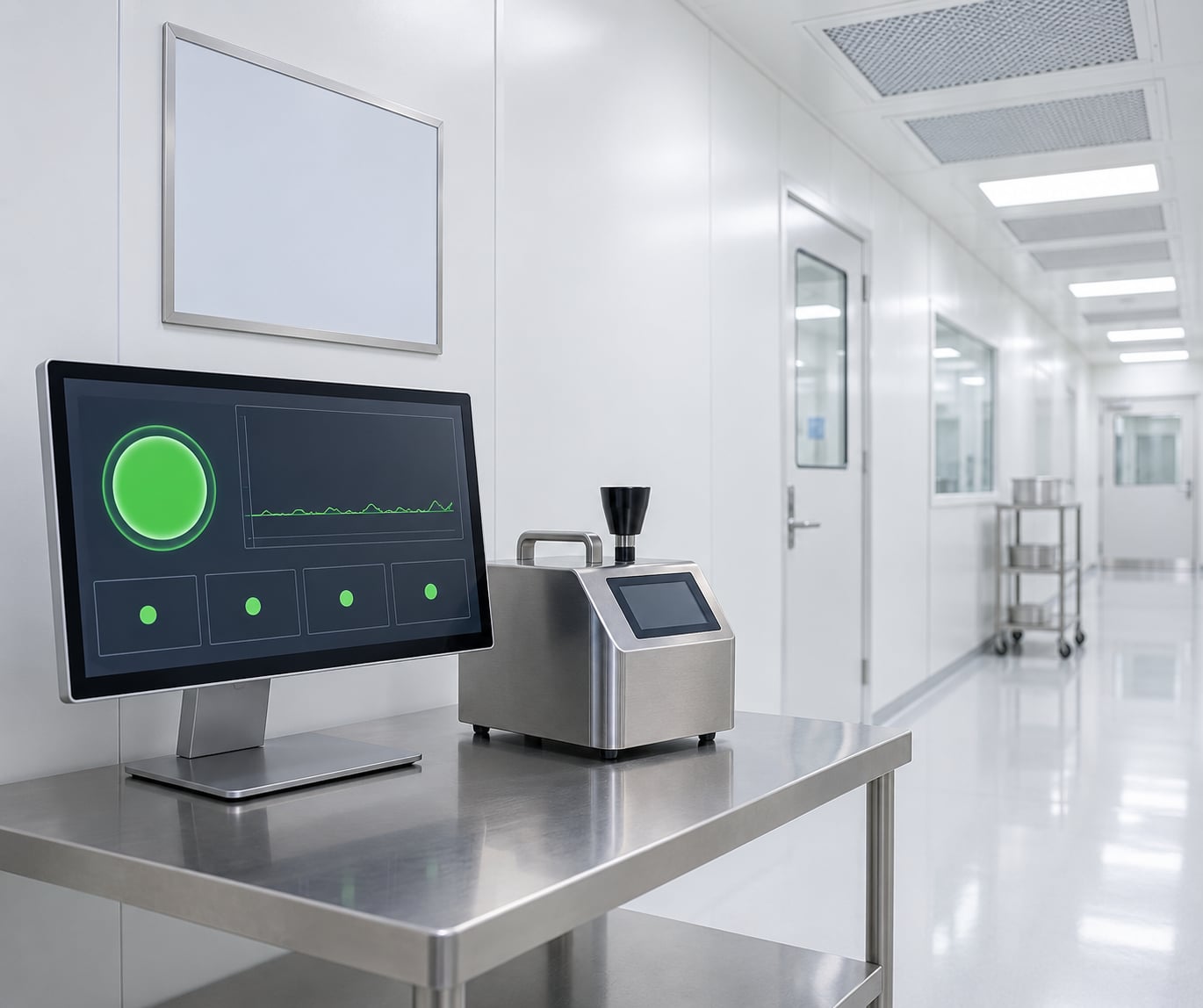
Cleanroom class ratings are ISO 14644-1 designations, running from ISO 1 to ISO 9, that set the maximum concentration of airborne particles allowed in … Read more
Think of chip making as repeated printing. A machine shines light through a stencil onto a light-sensitive coating on a silicon wafer, and where … Read more
If you are specifying an etch step for a wafer process, the short version of wet etch vs dry etch in semiconductor manufacturing is … Read more
Plasma etching is a dry etching technique that removes material from a semiconductor wafer using an ionized gas, excited by radio-frequency power. Reactive neutral … Read more