Metrology and Inspection in Chip Fabs Explained (2026)
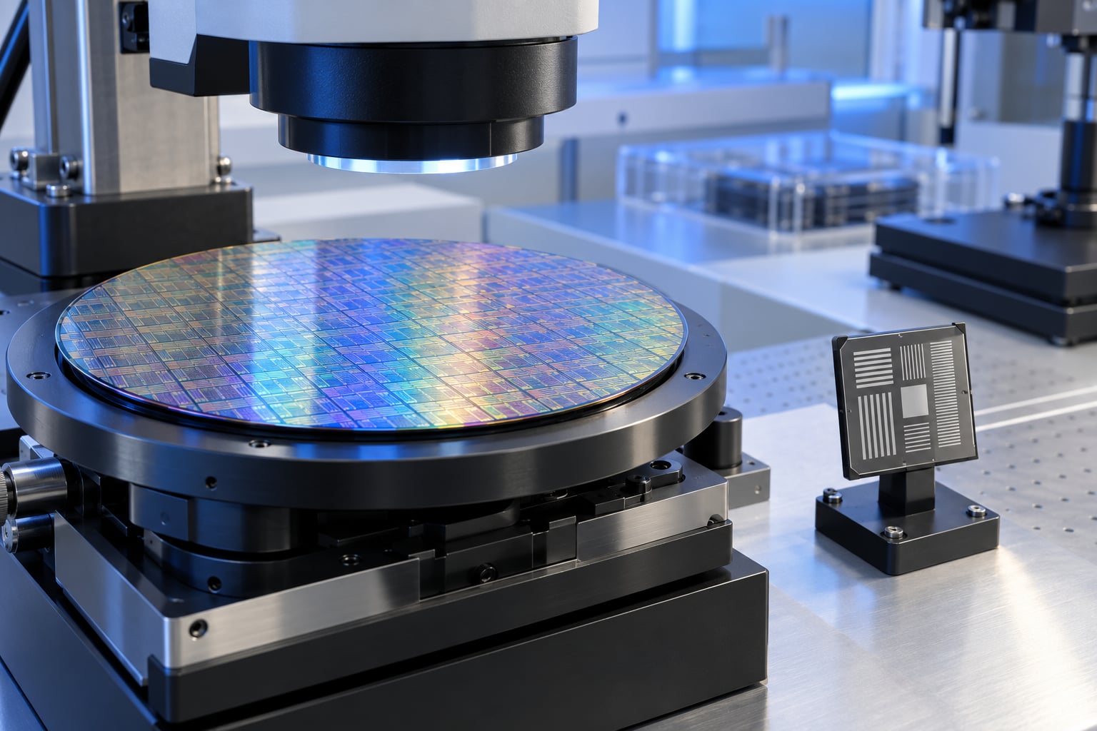
Metrology and inspection in chip fabs explained starts with one simple split: metrology measures a known process parameter, and inspection looks for something that … Read more

Metrology and inspection in chip fabs explained starts with one simple split: metrology measures a known process parameter, and inspection looks for something that … Read more
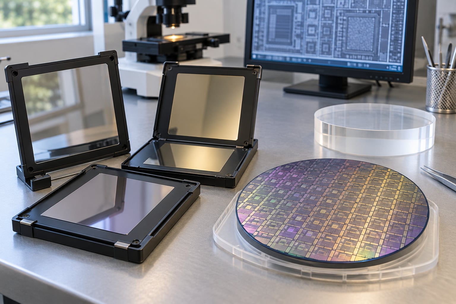
A mask set is the complete, matched group of photomasks a single chip design needs, one for every lithography layer, written and shipped together … Read more
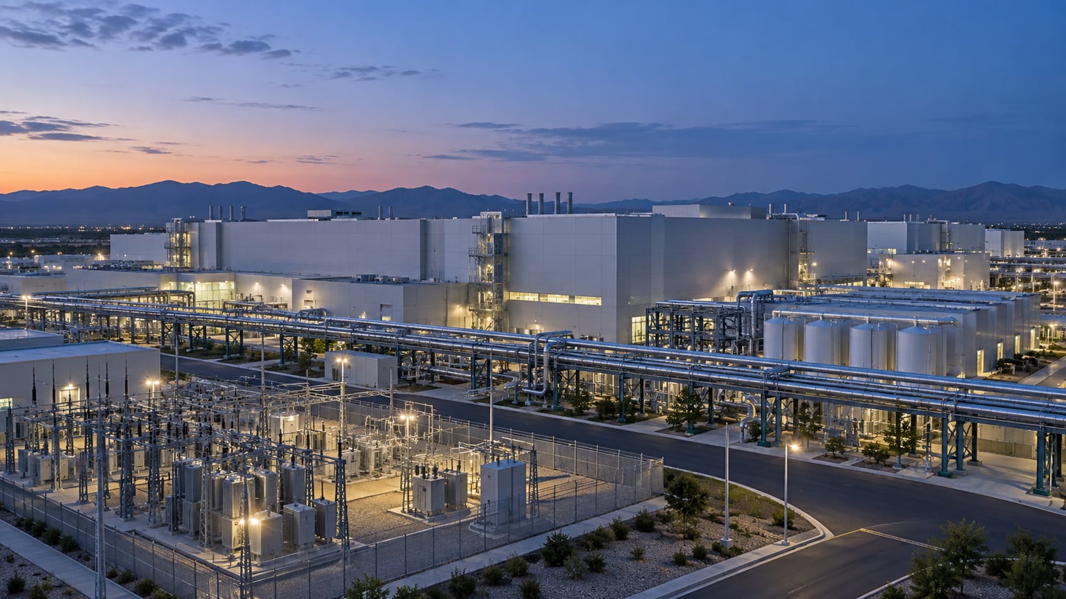
How much electricity does a semiconductor fab consume? A large 12-inch (300mm) fab draws roughly 100 megawatt-hours every hour, which is a continuous load … Read more
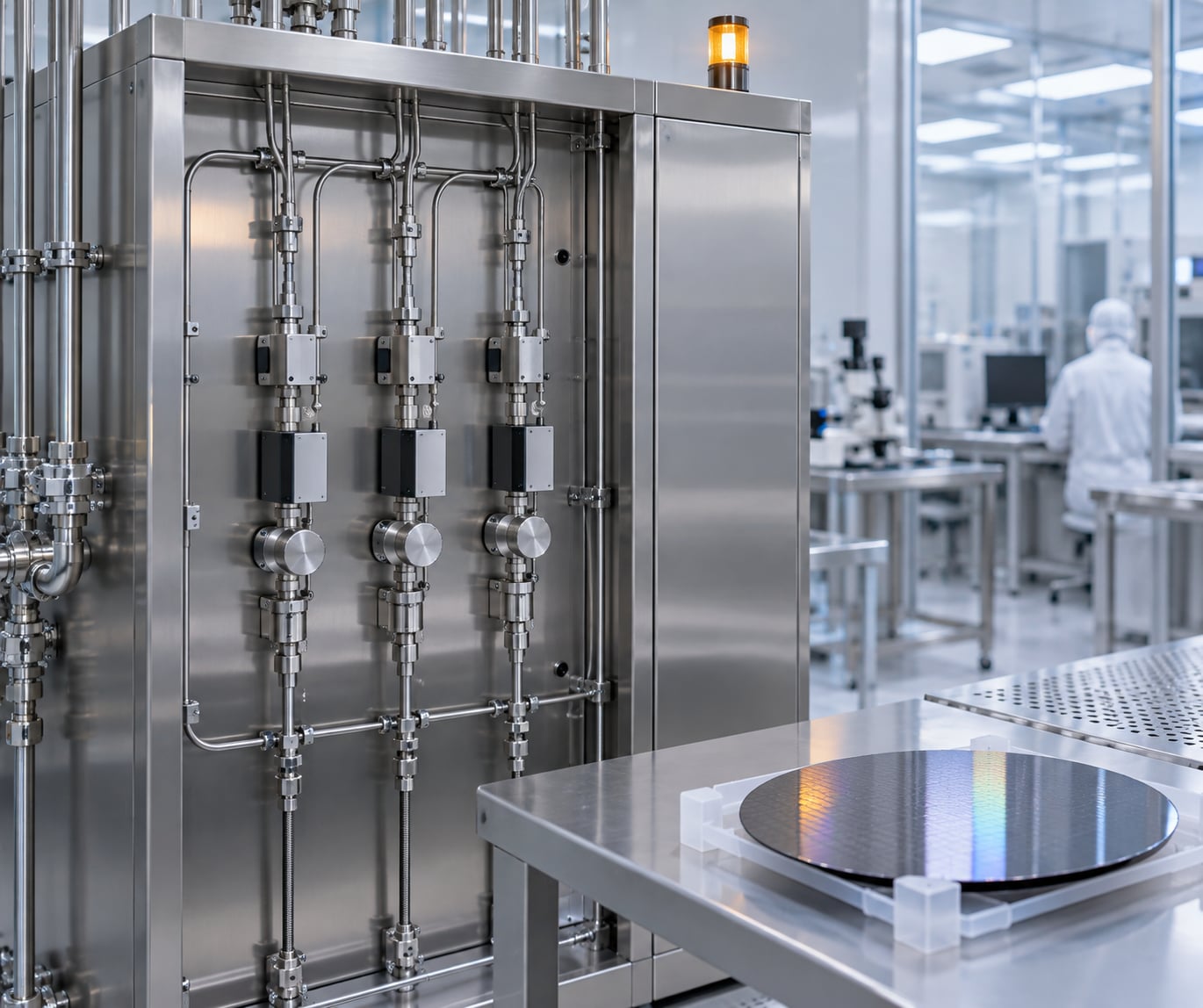
What gases are used in chip manufacturing? Chip fabs run on ultra-high-purity process gases grouped into five functional families: deposition, etching, dopant, chamber cleaning, … Read more
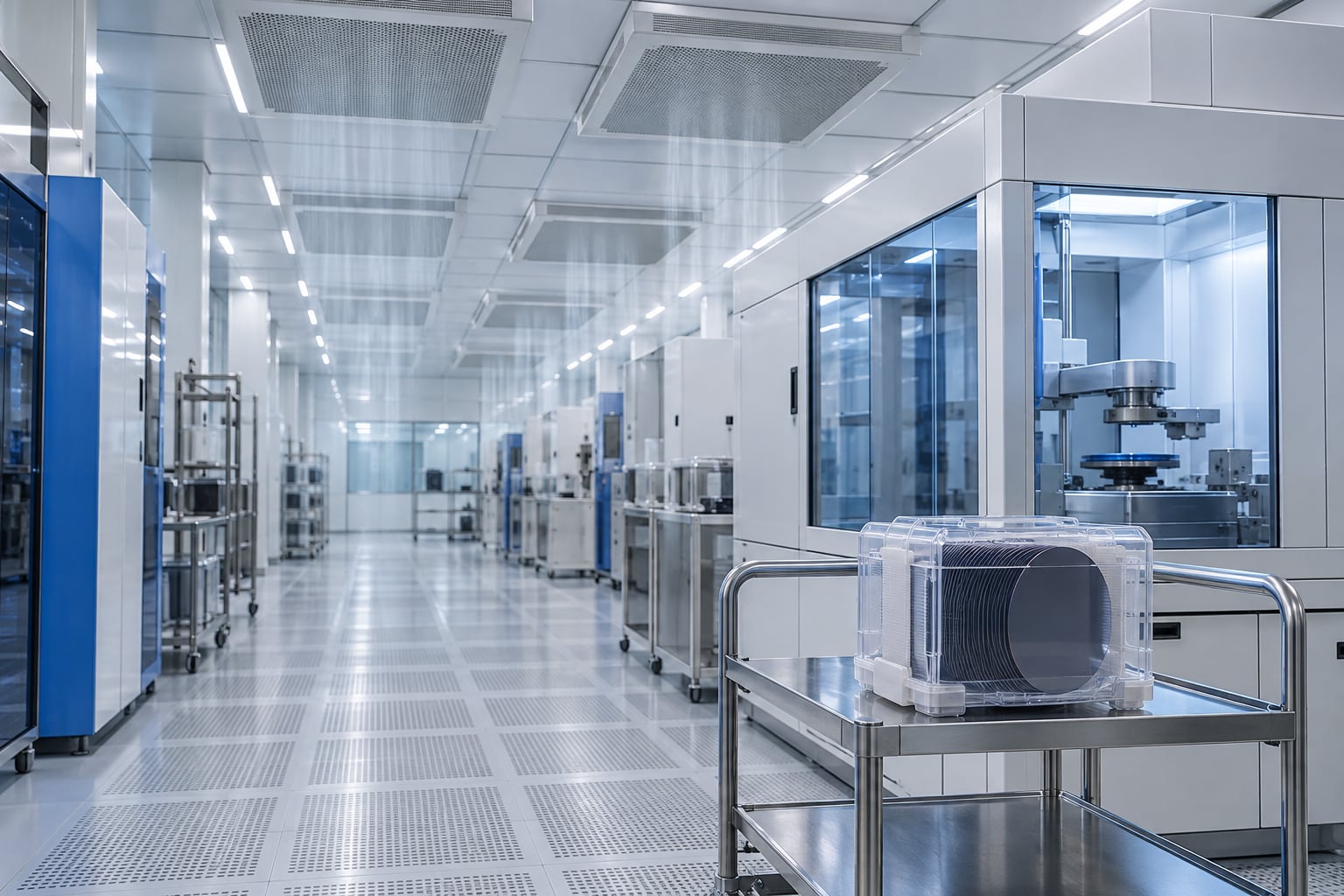
Contamination control in a semiconductor fab is the coordinated set of engineering and operational measures — cleanroom design, ultra-high-purity chemical and gas delivery, particle-controlled … Read more
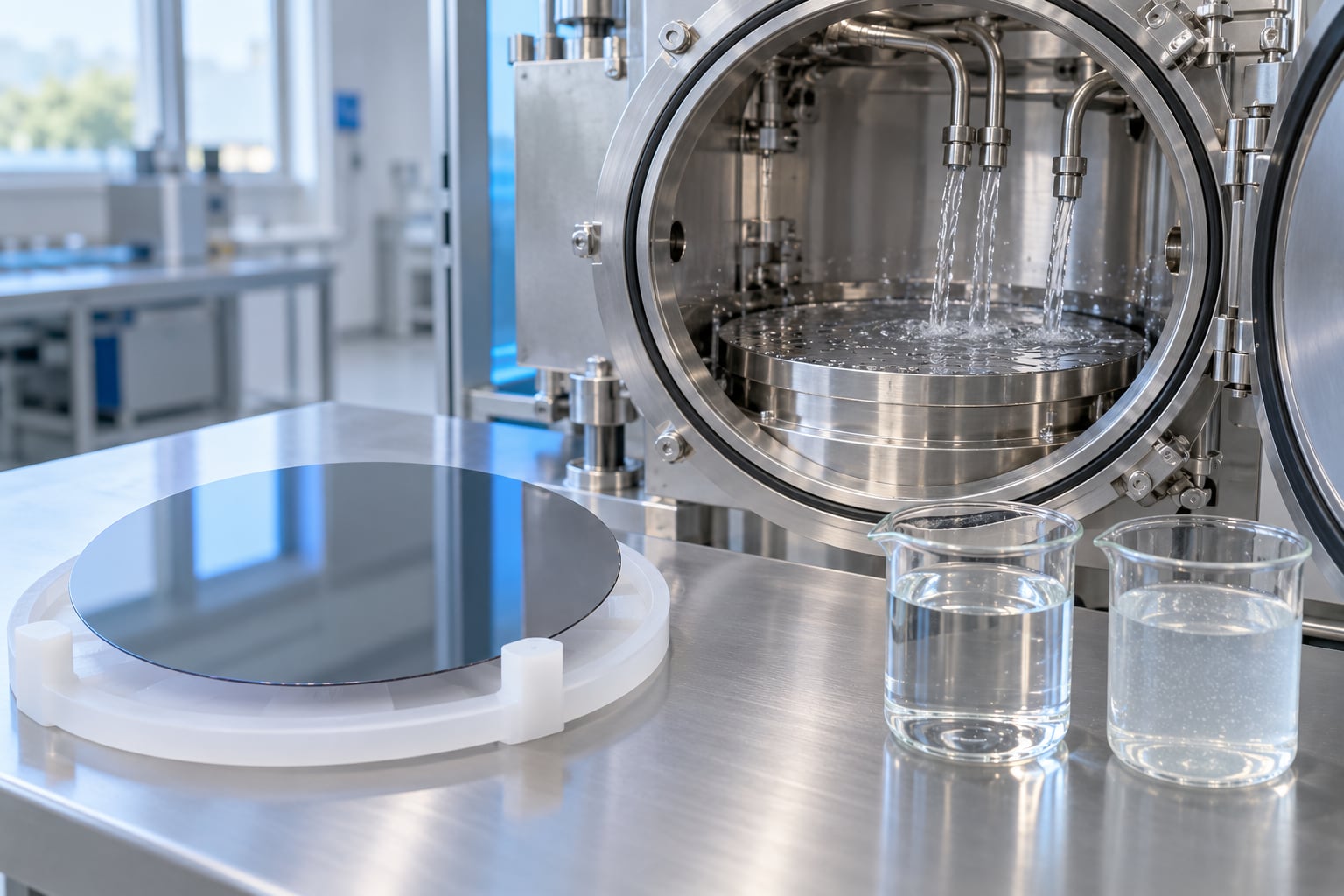
Why fabs use ultrapure water is simple: the wafer surface is the product, and any particle, metal ion, silica colloid or organic film that … Read more
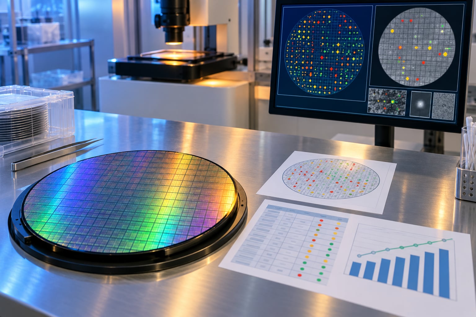
Defect density explained for chip manufacturing comes down to one number: the average number of defects per square centimeter of wafer area, usually written … Read more
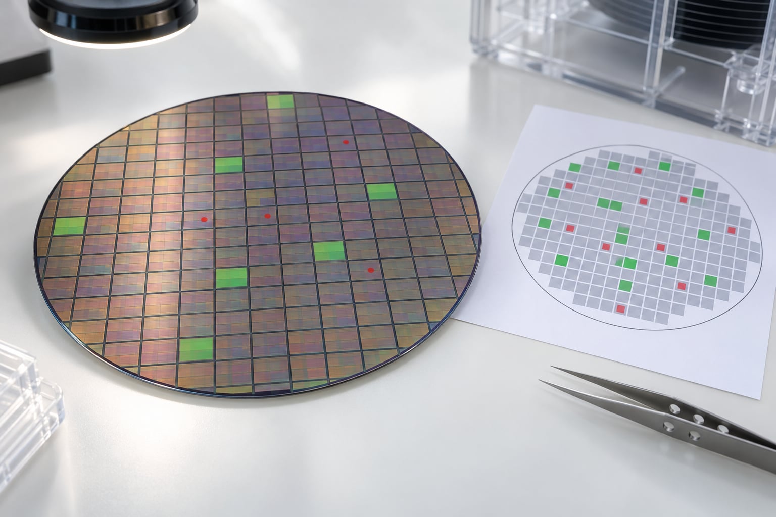
The short version of how semiconductor yield is calculated is one division: the number of functional (good) dies divided by the total number of … Read more
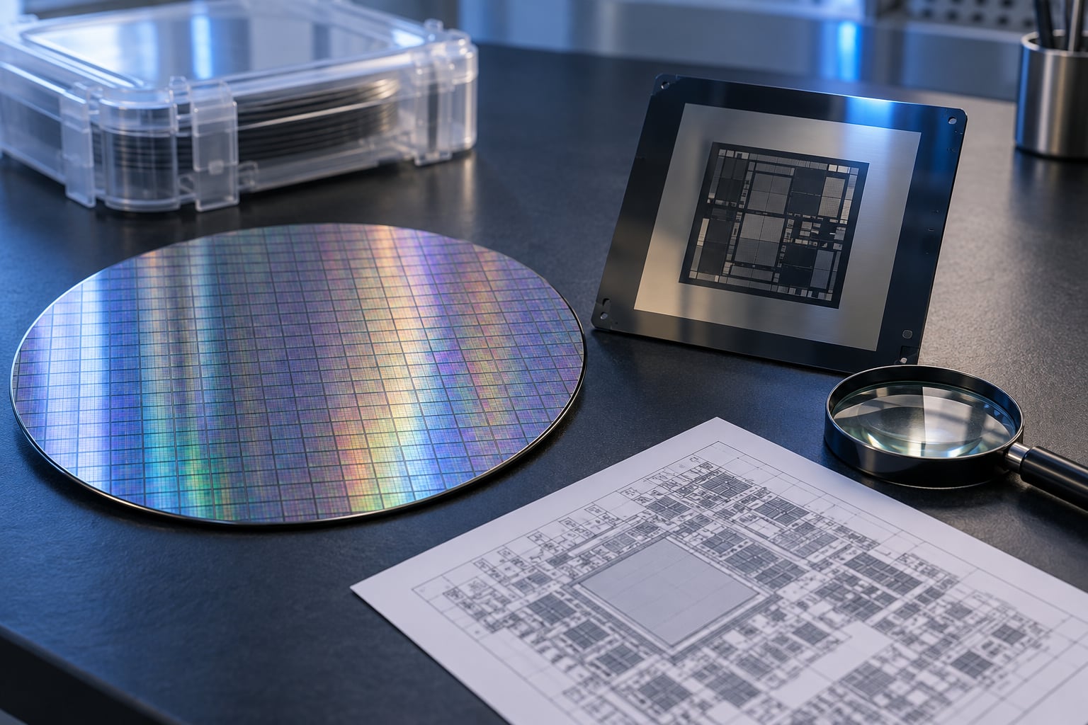
A semiconductor foundry is a company that manufactures chips other companies designed. It takes a finished layout file, prints that layout onto silicon wafers … Read more
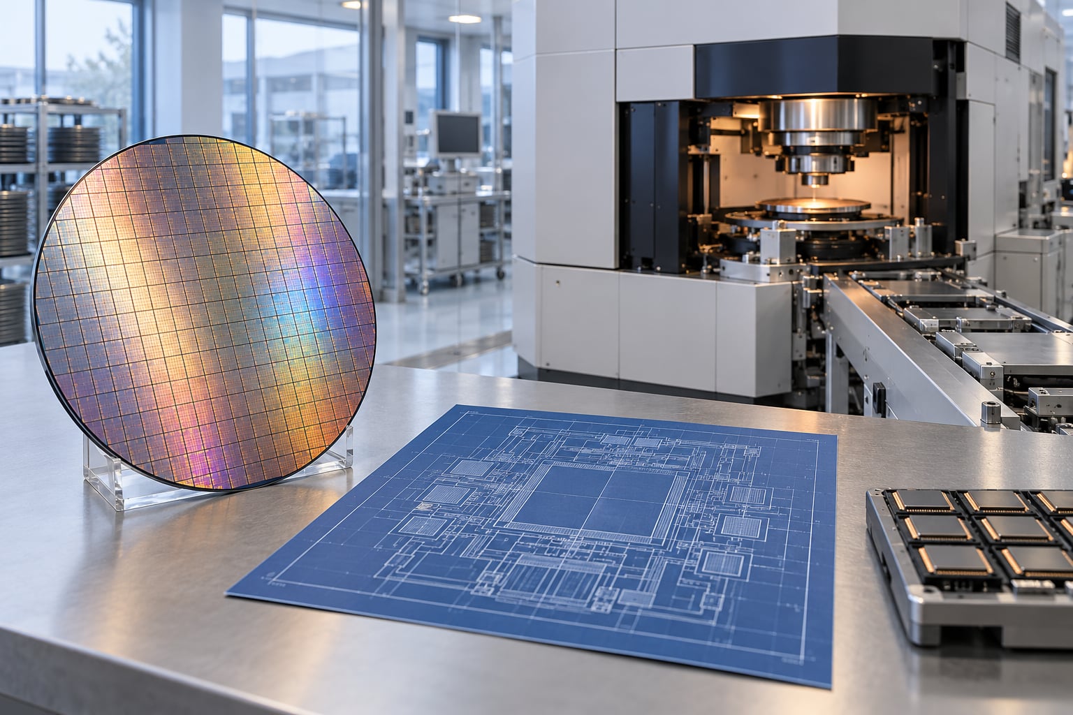
A foundry builds chips that other companies designed, a fabless company designs chips but owns no factory, and an IDM does both under one … Read more