A semiconductor foundry is a company that manufactures chips other companies designed. It takes a finished layout file, prints that layout onto silicon wafers through hundreds of cleanroom process cycles, probes every die on the wafer, and ships the wafers out for packaging before returning working parts. If you have been wondering what a semiconductor foundry actually does with your design, the short answer is that the foundry owns the factory, the process, and the masks, and it turns your drawing into silicon.
That framing matters because most of the confusion around this industry comes from mixing up words. A fab is a building. A foundry is a company that runs fabs for customers. An integrated device manufacturer, or IDM, does both and sells its own chips. Once those are separated, the rest of the industry becomes much easier to follow.
Updated for 2026, this guide walks a chip from the first layout handoff to the packaged part that ships to a distributor.
Table of Contents
- What a Semiconductor Foundry Actually Does
- Where a Foundry Fits in the Chip-Making Process
- How a Foundry Takes a Design Into Manufacturing
- What Happens Inside a Semiconductor Fab
- The Main Services a Foundry Provides
- Why Process Nodes and Yield Matter
- How a Foundry Tests and Ships Finished Chips
- What a Foundry Does Not Do
- How Foundries Make Money
- How to Evaluate a Foundry for a Chip Project
- Frequently Asked Questions
- What is a pure-play foundry?
- What is the difference between a fab and a foundry?
- What are the steps in the semiconductor manufacturing process?
- How long does it take a foundry to make a chip?
- Does the United States make semiconductor chips?
- Is semiconductor manufacturing bad for the environment?
- Conclusion: Start with the Process
What a Semiconductor Foundry Actually Does
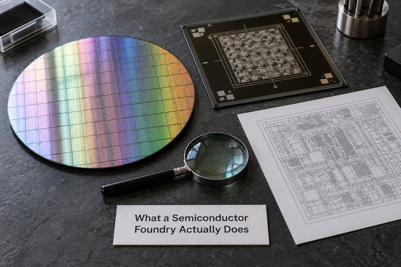
A semiconductor foundry is a contract manufacturer for integrated circuits. It develops its own recipes for building transistors on silicon, and sells that manufacturing capability to any customer willing to follow its design rules. The customer’s chip is only one product running through the same line as hundreds of others, which is why a single fab can serve thousands of designs at once.
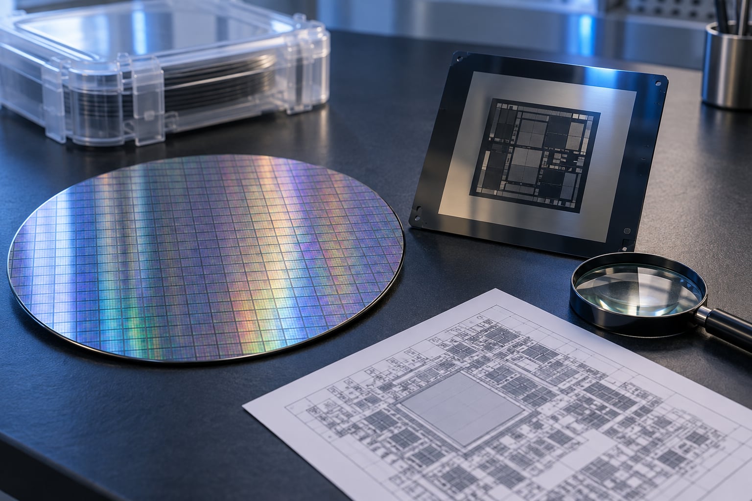
The foundry receives three things from a customer: a GDSII or OASIS layout database containing the full geometric description of every layer, a purchase order for wafers, and the finished tape-out order. What comes back is a tested wafer, or a packaged part once an assembly and test house has done its work.
Put plainly, a foundry does the following:
- Publishes a process technology and a process design kit that defines what can be built.
- Checks the customer layout against design rules for manufacturability before making any masks.
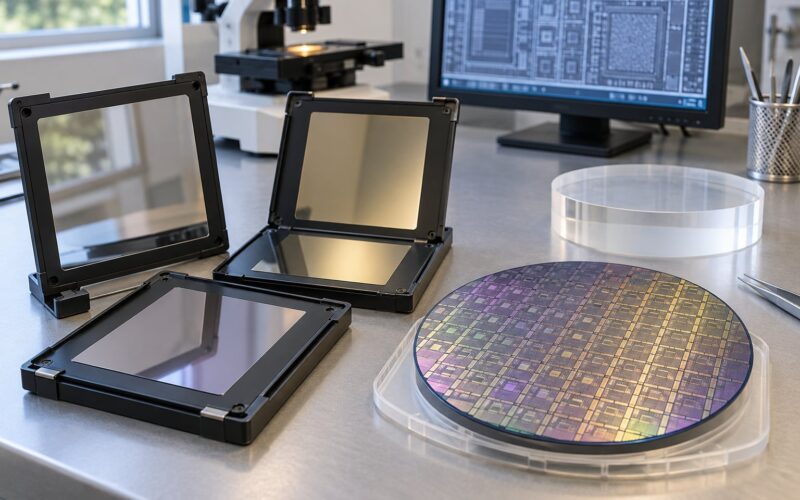
- Orders or reuses a photomask set that transfers the layout pattern onto resist.
- Runs wafers through repeated deposition, lithography, etching, doping, polishing and cleaning cycles.
- Measures defect density and controls the process so that yield climbs over the life of a product.
- Probes each die electrically on the wafer and marks the good ones.
- Ships wafers to an outsourced assembly and test provider, or performs that step in its own facility.
- Delivers parts that meet the reliability, quality and delivery commitments written into the contract.
Now the terminology that trips people up. These five models are frequently used interchangeably in press coverage, but they describe different businesses.
| Business model | Designs chips? | Owns a wafer fab? | Sells its own products? | Examples |
|---|---|---|---|---|
| Fabless | Yes | No | Yes | Apple, Qualcomm, Nvidia |
| Pure-play foundry | Minimal | Yes | No | TSMC, GlobalFoundries, UMC |
| IDM | Yes | Yes | Yes | Samsung, Intel, Texas Instruments, Micron |
| Fab-lite | Partly | Yes, part of a larger operation | Yes | Intel Foundry, Samsung Foundry |
| OSAT | No | No wafer fab | Sometimes | ASE, Amkor, JCET |
A foundry serving Apple and a foundry serving a two-person startup are running the same line of business. The difference is volume, not function.
Where a Foundry Fits in the Chip-Making Process
The customer journey runs from a design file to a working part, and only some of it belongs to the foundry. Here is the sequence, with the owner of each step marked.
- Architecture and design. The customer defines the block diagram, writes RTL, and places and routes the logic using an electronic design automation tool such as Cadence or Synopsys. The customer owns this step.
- Process selection. The customer picks a foundry and a node based on speed, power, area, cost and capacity. The customer owns the decision, the foundry publishes the options.
- Design for manufacturability and signoff. The customer runs the layout against the foundry’s process design kit, fixes rule violations, and signs off on timing and power using the standard-cell libraries and memory models supplied in that kit. Customer work, foundry-supplied data.
- Mask order and data prep. The foundry takes the layout, applies optical proximity correction and process compensation, writes the mask data, and orders a photomask set. Foundry work.
- Wafer fabrication. The foundry runs wafers through the full front-end process. Foundry work.
- Wafer sort. The foundry probes each die, applies its own test limits, and marks good and bad die. Foundry work.
- Assembly and final test. Wafers move to an OSAT that dices, packages and tests the parts, or to a foundry’s own back-end line. Split ownership.
- Shipment and production ramp. Finished parts go to the customer’s distributor or assembly partner, and repeat orders flow back into the same process. Both parties.
Practitioners describe the relationship in much the same way: you hand over a layout and receive tested, packaged parts weeks later, and the foundry owns essentially every process decision in between. The community view is that the quality of the process design kit and its design rules matters more to a small team than node leadership.
How a Foundry Takes a Design Into Manufacturing
The handoff is formal and unforgiving, which is why it deserves its own walkthrough.
First, the customer installs the process design kit, or PDK. The PDK is the foundry’s rulebook expressed as files: standard-cell libraries with real timing and power numbers, memory compiler models, parasitic extraction models, the design rules deck, and the layer stack definition. A design placed against the wrong PDK simply will not work.
Second, the layout is checked against design rules for density, spacing, antenna ratios, minimum enclosure and every other geometric constraint. Violations are fixed in the customer’s environment.
Third, the design goes through timing and power signoff, where the tool reports critical paths and current draw using the PDK’s characterised cells rather than estimates.
Fourth, when the design is clean, the customer places a tape-out order. That is the point of no return: the layout file is frozen and a mask set is ordered, which is one of the largest fixed costs in the whole project.
Fifth, the foundry performs mask data preparation. Optical proximity correction reshapes features so they print correctly at the lithography wavelength, and the foundry checks the mask against the original layout for defects. A mask error here can scrap an entire wafer batch.
Sixth, the design is added to the process queue and receives wafer starts, measured in batches rather than individual pieces. The lot size is usually committed at the tape-out order, which is why early demand estimates matter.
What Happens Inside a Semiconductor Fab
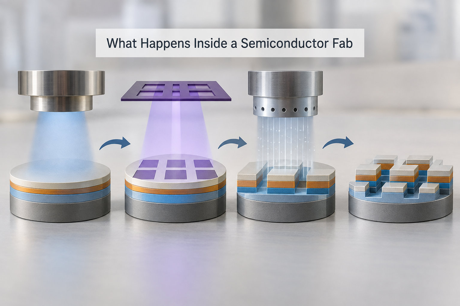
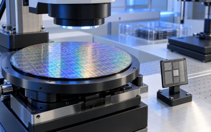
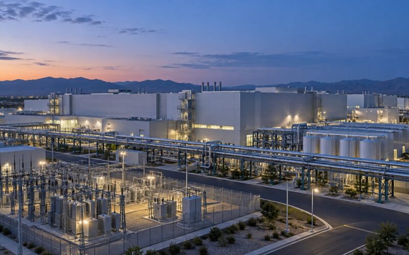
The fab is a cleanroom full of machines that add, remove and pattern material on the surface of a silicon wafer. Nothing is sculpted in three dimensions. A modern chip is built by stacking and patterning many extremely thin layers, then drilling contacts between them, and each of those layers requires a small set of repeated operations.
The core cycle has about half a dozen moves. Oxidation grows a thin insulating layer on the silicon. Deposition lays down a film of oxide, nitride or metal. Photolith coats the wafer in resist, bakes it, focuses light through a reticle to project the mask pattern, and develops the resist so the pattern survives. Etching removes the exposed material underneath. Ion implantation fires ions into the silicon to change its electrical properties. Chemical mechanical planarization polishes the surface flat again, and cleaning washes away residue between steps. Metrology and inspection tools from vendors such as KLA check the result continuously.
That cycle does not run once. It runs for hundreds of layers, with each of the thousands of individual steps tracked against the process recipe. A single advanced chip can involve well over a thousand process steps, and the wafer spends weeks moving through the tool set, sometimes several times as features are built upward.
Two practical consequences follow. First, wafer fabrication is front-end work; everything from here to the finished part is back-end work. Second, because a lot moves as a unit, a single contaminated tool can affect dozens of wafers at once. That is why cleanroom class, air filtration and particle control dominate the cost structure of a modern fab, and why contamination control is the foundry’s core competency rather than a side concern.
The Main Services a Foundry Provides
Manufacturing capacity is the headline service, but it is rarely the whole contract. A typical foundry relationship covers the following.
Process technology. The transistors, interconnect and memory options the foundry is qualified to build, offered in a family of nodes so a customer can trade area against speed and power without switching foundries.
Mask services. Mask data preparation, optical proximity correction, mask inspection, and either a new mask set or a stored one reused across multiple tape-outs of the same design.
Design enablement. Application engineers who help place a design, resolve rule conflicts, and close timing before wafers are ever started. This is often the least visible and most valuable service.
PDK and IP access. The process design kit, standard-cell libraries, and pre-verified interface IP such as SerDes, memory controllers and protocol blocks that shorten design time.
EDA support. Certified flows, reference designs and tool configurations that let the customer’s Cadence or Synopsys environment run predictably on that process.
Test and packaging services. Wafer probe and probe card development, burn-in, and in some cases in-house assembly and final test, or a managed handoff to an OSAT partner.
Volume and lifecycle support. Capacity commitments, forecast management, and the ability to keep a mature node running for a decade after a product has shipped.
The equipment supply chain runs alongside all of this. ASML supplies the extreme ultraviolet lithography systems used at advanced nodes, while Applied Materials, Lam Research and KLA supply deposition, etch and inspection tools that fill the rest of the line.
Why Process Nodes and Yield Matter
A process node name such as 7nm, 5nm or 3nm is a marketing label attached to a generation of transistor design. It no longer maps neatly to a physical dimension, so treat it as a version number. What the version reliably tracks is how much circuitry fits, how fast it runs, and how much it draws.
| Node family | Transistor style | Typical designs | Main trade-off |
|---|---|---|---|
| 3nm and 2nm | Gate-all-around | Flagship phones, AI accelerators | Highest mask, tooling and design cost |
| 5nm and 4nm | FinFET | High-volume mobile and compute | Strong performance, mature learning curve |
| 7nm | FinFET | Established flagship designs | Proven yield, wide IP availability |
| 28nm and above | Planar bulk | Automotive, industrial, analog, microcontrollers | Lower cost per die, high-voltage options |
Yield is the other half of the story. Yield is the share of dies on a wafer that meet specification. A design that costs the same to make on two nodes can differ by a factor of several in cost per good die purely because one process yields more working chips per wafer. That is why a smaller node is not automatically the right choice.
Most of the world’s chips sit on mature nodes, and for good reasons. Analog, power, automotive and microcontroller parts often need features that shrink with scale: high voltage tolerance, precise resistors, embedded non-volatile memory. Those products also ship in volumes large enough that wafer cost dominates. Leading-edge nodes win on power and area; mature nodes win on cost per function and on the availability of qualified tools and third-party IP.
How a Foundry Tests and Ships Finished Chips
Fabrication ends with a wafer full of untested dies, and nobody ships those. Testing starts while the wafer is still whole.
During wafer sort, a probe card with thousands of microscopic needles lands on the wafer and touches the pads of each die in turn. The test program applies voltage, clocks and signals, then records what passes, what fails and how close the marginal parts are to their limits. Good die are marked; bad die are left unmarked. Because testing this early is far cheaper than testing after packaging, foundries probe before they ship.
Some parts then go through burn-in, where they run at elevated voltage and temperature for hours or days to surface early-life failures that a brief test would miss. Automotive and industrial parts are commonly qualified this way.
The wafers go to the back end. They are thinned from a few hundred micrometres down to roughly half a millimetre so they can fit in a package, then diced into individual die. Assembly places each die in a package with bond wires or solder bumps connecting it to the leads, and final test runs the same electrical tests again on the finished part at system-level conditions. Trim, mark and inspection complete the process, and the parts ship.
Where that happens is the customer’s choice. Many designs go to an OSAT such as ASE, Amkor or JCET. Some foundries offer their own back-end lines or qualify specific assembly partners, and advanced packaging is increasingly part of the foundry sale because chiplet designs need interposers and advanced substrates that sit closer to the front end than to a traditional package house.
What a Foundry Does Not Do
Expectations get damaged here, so it is worth being blunt. A foundry does not design your chip. It does not decide your architecture, pick your target market, or tell you what to build. It does not own the intellectual property in your layout; that stays with the customer, and IP leakage was one of the original reasons the pure-play model existed in the first place.
A foundry also does not guarantee that a design will work commercially. It guarantees that a wafer built to its specification will meet its electrical, reliability and delivery commitments. If the design has a logic bug, the process will reproduce that bug faithfully on every one of the twenty thousand die.
The other half of what a semiconductor foundry actually does is absorb work the customer should not have to do: process development, mask making, contamination control, defect detection, test program development, and yield improvement over years. Many providers also offer design support and IP precisely because a well-supported design is cheaper for them to build and more likely to reach volume.
How Foundries Make Money
Foundry revenue has two halves, and the first one surprises people who assume wafer cost is everything.
Mask and setup charges. A tape-out carries non-recurring engineering costs: the mask set, mask data prep, engineering wafers, and the foundry time to qualify the design. These are charged once, and they are the single largest barrier for a small team. Advanced nodes cost far more here than mature ones.
Per-wafer pricing. Volume production is sold by the wafer or the lot, with pricing that reflects the node, the wafer size, the layer count and how much capacity the customer has committed. A customer that reserves capacity or signs a long-term agreement gets better terms and better priority during tight periods; one that buys a few hundred wafers pays list pricing.
Around those sit specialty premiums, where a process with unusual features such as high voltage, embedded memory, photonics or radio-frequency components commands more. Assembly and test fees are usually separate line items, either from the foundry’s own back end or from an OSAT partner.
Two economic facts explain most of the industry’s behaviour. A fab costs billions to build and must run near full utilisation to make sense, so foundries compete hard for volume commitments rather than for walk-in business. And the leading-edge side is close to a monopoly on supply, which is why a handful of firms can set the commercial terms for nearly every new chip design.
How to Evaluate a Foundry for a Chip Project
If you are choosing where to fabricate, here is the checklist that separates a workable relationship from a painful one.
- Process fit. Does the node meet your speed, power and area targets, and does the process support the analog, memory or high-voltage features your design needs?
- PDK and design rules. Are the libraries well characterised, are the rules stable across revisions, and does the flow run cleanly in your EDA environment?
- IP ecosystem. Are the interface blocks you need already available and verified, or will you have to build them?
- Design enablement. Will an application engineer actually review your design before the mask is ordered, and how fast do they respond?
- Capacity and lead time. Can they commit to a predictable number of wafer starts per month, and what happens to your lead time when the line is full?
- Yield track record. Ask for reference products on the same node and the yield curve they reached over the first year.
- Reliability data. Are automotive and industrial qualifications available on this process, and what documentation comes with them?
- Packaging options. Can they supply the package you need, or do you want to own that relationship separately?
- Geographic and policy risk. Where the fab sits, and how many other customers depend on the same site.
- Total cost. Mask charges, wafer price, minimum order quantity, and the cost of a second mask set if you need one later.
The short version matches what practitioners say out loud: for most design teams, PDK quality and design support beat raw node leadership. A well-supported 7nm design that ships beats an unsupported 3nm design that slips.
Frequently Asked Questions
What is a pure-play foundry?
A pure-play foundry manufactures chips for other companies and does not sell products of its own. TSMC, GlobalFoundries and UMC are the standard examples. The model separates design from manufacturing, so a company can build advanced silicon without funding a fab, and a foundry can fill its tools with work from many unrelated customers.
What is the difference between a fab and a foundry?
A fab is the physical facility where wafers are fabricated, with the cleanrooms, lithography tools and process equipment inside it. A foundry is the company that owns and operates those fabs and sells the manufacturing service to customers. One company can run several fabs, and one fab can contain process lines serving many foundry customers.
What are the steps in the semiconductor manufacturing process?
Silicon wafers are repeatedly cycled through oxidation, deposition, photolithography, etching, ion implantation, chemical mechanical planarization and cleaning, with metrology checking the result at every stage. After hundreds of layer cycles, each die is probed on the wafer during wafer sort, then the wafer is thinned, diced, packaged and given a final electrical test before shipment.
How long does it take a foundry to make a chip?
A wafer spends several weeks moving through the fab, because it returns to the lithography and etch tools hundreds of times across the full layer stack. Wafer sort, packaging and final test add more time, so a typical production order lands in the two to three month range. The very first wafers of a new design also run below target yield while the process is tuned.
Does the United States make semiconductor chips?
Yes. Intel operates large fabs in the United States, GlobalFoundries runs facilities in New York and Vermont, and TSMC, Samsung and Texas Instruments are building or operating US capacity with government support under the CHIPS Act. The newest plants target leading-edge and mature nodes, so domestic output is growing from a low base as these fabs come online.
Is semiconductor manufacturing bad for the environment?
It is intensive rather than unique in kind. A modern fab consumes a great deal of ultrapure water for wafer rinsing and cleaning, a large share of a fab’s electricity budget goes to the cleanroom and process tools, and it produces acidic and caustic chemical waste that must be treated. Foundries have cut per-wafer water use sharply through recycling, and abatement systems reduce chemical emissions, but the total footprint remains high.
Conclusion: Start with the Process
A semiconductor foundry converts someone else’s layout into working silicon, and it owns every physical step between the tape-out order and the tested wafer. Once you can separate the fab from the foundry, the foundry from the IDM, and the OSAT from all three, the industry stops being mysterious and starts being a supply chain you can reason about. The first move in any chip project is to match your design, performance, power, cost and volume requirements to a process technology, then pick the foundry whose rules, tools and capacity line up with it.