Overlay error is the unwanted positional difference between a lithographic layer and the layer it is supposed to sit on top of. It is the failure of pattern placement accuracy, measured in nanometers and reported as an X/Y offset at points across the wafer. This guide explains what the term means, how it is measured, where it comes from, and how process engineers pull it back inside spec.
If you have just started working in a fab or a mask shop, you will run into the word everywhere: in SPC charts, in yield excursion reports, in the overlay correction section of a scanner recipe. Nobody bothers to define it because everyone assumes you already know. That assumption is why so much of the published material on overlay is either paywalled or written for people who already spent a decade inside a cleanroom.
Table of Contents
- What Is Overlay Error in Lithography?
- How Is Overlay Error Measured on a Wafer?
- What Are the Main Types of Overlay Error?
- What Causes Overlay Error?
- How Does an Overlay Correction System Reduce the Error?
- How Do Engineers Set Overlay Tolerances?
- How Do You Troubleshoot an Overlay Failure?
- Frequently Asked Questions
- What is overlay error in lithography?
- How is lithography overlay error measured?
- Does a zero overlay mean value guarantee good lithography?
- What is the difference between overlay error and CD error?
- Why does overlay error vary across a wafer?
- Can overlay error be corrected without changing the mask?
- Conclusion
What Is Overlay Error in Lithography?
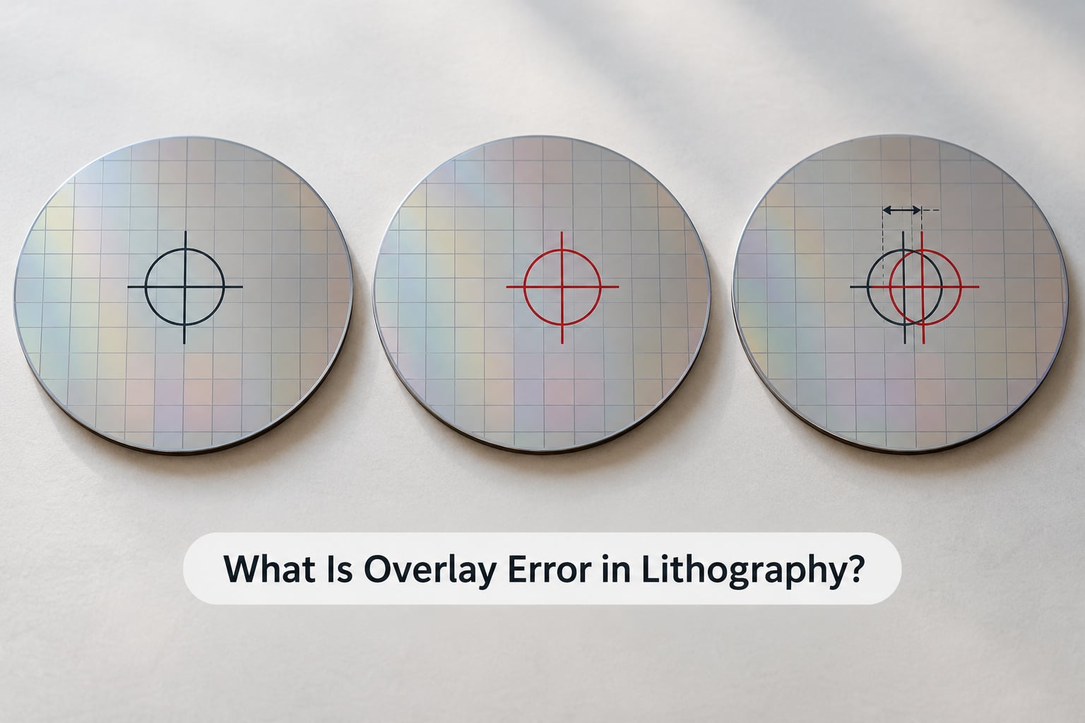
A chip is built by printing one layer, processing it, and then printing the next layer on top of the result. Overlay error is the distance between where the new pattern actually landed and where it was supposed to land relative to the layer underneath. Because a chip is flat, that distance has only two in-plane components: X and Y. There is no Z component to correct for in a two-dimensional overlay measurement.
What overlay error means in practice is simpler than the vocabulary around it. Every exposure prints alignment marks alongside the circuit pattern. After develop, a metrology tool finds those marks, finds the matching marks from the previous layer, and subtracts one position from the other. That subtraction, in nanometers, is the overlay error at that point.
It is worth separating overlay from the other errors that show up on the same wafer map, because they get confused constantly.
- Focus error changes line width. A defocused line is wider or narrower, but it can still be printed in exactly the right place.
- Dose error also changes line width and profile, for the same reason.
- CD error is the critical dimension error, the size of a feature versus its target size. It is a width problem, not a position problem.
- Wafer placement error describes where the wafer itself sits on the chuck. It feeds into overlay but is a different measurement with a different owner.
- Overlay error is purely about position: pattern A did not print on top of pattern B.
Getting that distinction right early pays off later. If you chase a CD problem with overlay compensation, you will spend a week moving the wrong knobs.
Outside lithography, “overlay” gets used for other things entirely: a graphic laid over a photograph, a stencil laid over a road, an artist’s tracing. None of those meanings carry over. In a semiconductor context, overlay always means layer-to-layer registration.
How Is Overlay Error Measured on a Wafer?
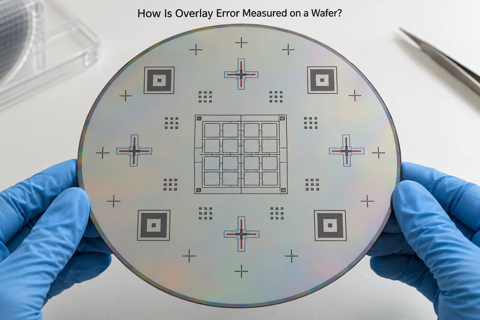
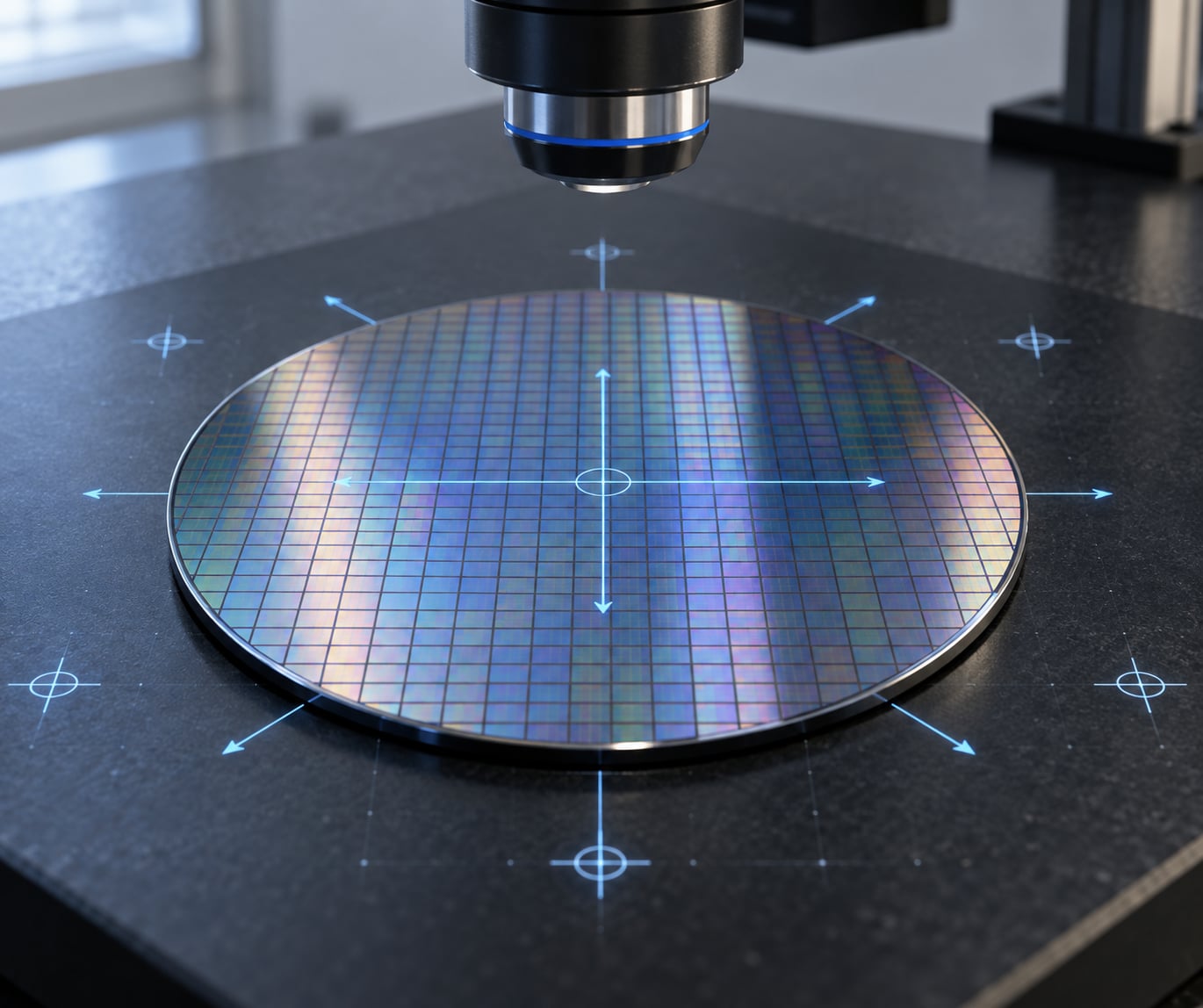
Measurement happens after exposure and develop. The tool, usually a dedicated overlay metrology platform working in visible or near-infrared light, scans the wafer for alignment targets and computes the offset between the current layer’s marks and the previous layer’s marks. The result is not one number. It is a vector field sampled at points across the wafer, and each point has its own X and Y value.
Three target styles cover most production work, and each one suits a different situation.
| Target style | How it works | Where it fits |
|---|---|---|
| Box-in-box | Nested squares read by edge detection in the four directions | Back-end and mature-node layers with relaxed specifications |
| Bar-in-bar | Four long bars read with a directional signal | Advanced layers, better resistance to process asymmetry |
| Grating or diffraction | Signal derived from a first-order diffraction peak, using short wavelengths | EUV layers where a classic optical target can be too large |
Once you have offsets at each sample point, engineers report them in a few standard ways.
- Mean overlay is the average X/Y offset across the wafer. A tool can be perfectly consistent and still be systematically shifted.
- Uniform overlay describes how much the offsets vary from point to point. This is the number that actually breaks circuits.
- 3 sigma is the common specification convention: mean plus three times the standard deviation of the sampled offsets, quoted as a vector magnitude in nanometers.
- Vector magnitude combines X and Y into a single number, so a wafer with a small mean and a large spread still shows a large 3 sigma.
When a chip designer sees a per-layer or per-field number, it is the result of that process: sample points grouped by layer, then by exposure field within the scanner’s grid. Fields are the small rectangular exposure areas the scanner steps across, and because each field is corrected slightly differently, engineers report field-by-field values to see whether the correction is holding up across the reticle.
One practical caveat: overlay metrology is optical, and the exposure wavelength is much shorter. That mismatch limits how small a true offset the tool can resolve, and it puts a floor on measurement uncertainty well above zero. A number read at the metrology resolution limit deserves suspicion.
What Are the Main Types of Overlay Error?
Errors are usually classified by shape, and the shape tells you what kind of correction will work.
Translation is a uniform shift in one direction. The whole wafer moves a couple of nanometers along X. A constant offset like this is easy to correct: subtract it and print.
Rotation is a shift that increases with distance from the rotation centre, like the hands of a clock that are slightly too fast. Correction subtracts an amount proportional to radius, which is why a linear model handles it.
Magnification is a scale error. The pattern prints very slightly larger or smaller than intended, so the offset grows outward from the centre of the wafer. A first-order magnification term fixes most of it.
Higher-order error is whatever is left after translation, rotation and magnification are removed: bow, barrel, pincushion, and the wafer-edge behaviour that shows up as vectors that fan out or curl near the rim. This is where polynomial correction earns its keep. A fit that includes third, fifth or seventh order terms can absorb a shape that a linear model would leave behind, which is why tools that ship only linear correction usually show worse edge-of-wafer performance.
Random error is point-to-point scatter with no reproducible pattern. It cannot be corrected, only characterized and budgeted, because there is no model to fit.
Systematic error has a reproducible pattern. It is the part worth attacking, since a stable pattern can be learned and fed back into the next exposure.
On a vector map, translation shows as parallel arrows of equal length. Rotation shows as arrows whose length grows with radius. Magnification shows as arrows pointing outward or inward. Higher-order error shows as arrows that curve. If you can read the map, you already know which term to add to the correction model.
What Causes Overlay Error?
Error enters the process from three broad directions: the reticle, the exposure tool, and the wafer plus everything done to it. Most teams find that the third one is the one that ruins their week.
| Source | How it shows up | Usual owner |
|---|---|---|
| Wafer deformation and chucking | Edge-of-wafer vectors pointing outward, worst near the rim | Process integration |
| Process-induced film stress | A displacement signature that repeats lot after lot, often anti-correlated with a specific layer’s contraction | Process integration and CMP |
| Film thickness variation and CMP | Smooth radial or low-order vector shapes tied to layout density | CMP and etch |
| Etch-induced displacement | Pattern-dependent shifting, worse where large dense areas meet sparse ones | Etch |
| Track motion and thermal drift | Gradual drift across the lot as the track heats up, improving as the tool stabilises | Track and equipment engineering |
| Stage and scanner calibration | Tool-level offsets that persist across many lots, sometimes with a recognizable zone pattern | Scanner and stage engineering |
| Reticle placement and mask writing | A consistent offset for one specific mask and layer pair | Mask shop |
| Exposure and stage warming | Offset that grows with exposure count within a lot | Scanner engineering |
| Measurement noise and target asymmetry | Scatter without a repeatable shape, or an offset that moves when the target changes | Metrology |
Process-induced stress deserves its own paragraph because it surprises people. A film deposited or etched under tension can physically pull on the wafer, changing its shape in a way that shifts everything printed afterwards. Coherent gradient sensing has been used to map this surface displacement directly and correlate it against the resulting overlay, which turns “something is wrong” into a correction you can calculate before the next lot even runs.
EUV adds its own sources. Mask heating during exposure grows with accumulated dose, so a reticle sitting under the beam for a long exposure can drift slightly as a layer is written. Because the wavelength is short and the target geometry is demanding, a small thermal change matters more than it would at ArF immersion.
How Does an Overlay Correction System Reduce the Error?
Correction is a loop. It runs from measurement, through a model, to an adjustment applied at the next exposure, and then back to measurement again.
- The scanner prints alignment marks together with the layer pattern.
- Develop and any hard bake finish, fixing the printed geometry.
- The overlay metrology tool measures the marks and computes X/Y offsets at each sample point.
- The offsets are grouped into a vector field across the wafer.
- A correction model fits translation, rotation, magnification and higher-order terms to that field.
- The model outputs correction coefficients, usually called correctables.
- The scanner applies those correctables at the next exposure, stage by stage or field by field.
- The corrected layer is measured again to confirm the result.
Two control strategies use the same loop with different timing, and the difference matters when you are diagnosing a problem.
Feed-back waits for measurement. The wafer is already exposed, the data comes back, and the correction applies to the following wafer. It is simple and reliable but always one exposure behind, so it cannot fix anything on the wafer you just printed.
Feed-forward predicts the error before exposure. If you have a process fingerprint that maps process conditions to the displacement they produce, you can apply the predicted correction to the very next layer without waiting for measurement data. Studies of this approach report strong correlations between predicted displacement and measured overlay, which is what makes it usable in production.
Correction can be applied at different granularity: wafer-to-wafer for slow drift, within-wafer with a field or zone correction, or per-exposure for the fastest response. Finer granularity costs more throughput and more tool capability, so most processes settle on a mix.
How Do Engineers Set Overlay Tolerances?
A tolerance is never picked in a vacuum. It comes from the design margin, which is the gap between the printed features and the point where they would touch or separate. Every nanometer of overlay error spends part of that gap, so the specification is a shared decision between the design rules and the process integration team.
| Node | Typical overlay specification | Main driver of the difficulty |
|---|---|---|
| 28 nm | Around 7 to 9 nm | Process stress and basic stage accuracy |
| 14 nm | Around 4 to 5 nm | Film stress accumulation across more layers |
| 7 nm | Roughly 2.5 to 3 nm | Denser films, tighter contact and via overlaps |
| 5 nm | Around 1.5 to 2 nm | Edge-of-wafer wafer deformation |
| 3 nm and beyond | About 1 nm, with sub-1 nm in development | Measurement uncertainty approaching the process floor |
These are typical ranges rather than published standards, and every program negotiates its own numbers. They do show the trend clearly: as nodes shrink, the specification roughly halves each step, which means the overlay error the process allows is now a small fraction of the feature size it must hit.
Three factors move a specific layer’s tolerance away from the node average. First, pitch and pattern orientation. Alternating lines and spaces in one direction tolerate less error along that axis than they do across it, because the failure mode is a bridge between two lines rather than a gap closing.
Second, design rule choices. A designer who adds placement margin to a critical via or contact can trade a looser overlay spec for a slightly larger footprint, and plenty of programs do exactly that.
Third, metrology uncertainty. If your measurement repeatability is a meaningful fraction of your specification, you cannot tell a pass from a fail with confidence. Process capability indices like Cpk exist precisely to catch that situation before it reaches the customer.
One concept worth keeping separate: an overlay budget is not a specification. The budget is the internal allocation of nanometers across contributors, so the team knows which term to attack when the total drifts. The specification is the single number the customer of the process, usually the design organization, is held to.
How Do You Troubleshoot an Overlay Failure?
Work the sequence in order. The temptation is to jump straight to tightening a correction model, and that is usually the slowest path to an answer.
Confirm the measurement first. Check measurement noise and repeatability on the suspect layer. If the same wafer remeasured twice gives materially different offsets, you are debugging metrology, not process. Rule out target asymmetry by comparing a bar-in-bar target against a box-in-box target on the same layer; if the numbers disagree by a consistent amount, the target is the story.
Separate random from systematic. Look at the vector map. Scatter with no shape means random error, and random error is budgeted, not corrected. A clean, repeatable shape means you have something to model.
Read the shape. Uniform arrows mean translation, offset keyed to distance from centre means rotation or magnification, and a curl near the rim points at wafer deformation or chucking. Outward vectors that repeat on every lot usually mean process-induced stress rather than a tool problem.
Check field dependence. If the error varies field to field instead of wafer to wafer, look at the correction granularity in the recipe. A wafer-level correction applied to a zone-dependent error leaves the residual in the field map.
Check lot-to-lot behaviour. Drift within a lot points at thermal history: track warm-up, stage warm-up, or exposure dose accumulation. A shift that appears on one mask and layer pair only is a mask placement issue, and it goes to the mask shop.
Compare against electrical data last. If you suspect overlay is the root cause of a yield cliff, the confirmation is spatial. A yield signature that lines up with the wafer edge, with a high-stress layer’s footprint, or with a specific field of the reticle is overlay. A uniform yield loss across every layer and every position is more likely CD or a process defect issue.
Then, and only then, adjust. Tightening a correction model when the real cause is metrology noise just makes the tool chase its own measurement error.
Frequently Asked Questions
What is overlay error in lithography?
Overlay error is the positional difference between a printed lithographic layer and the layer beneath it, when the two should line up exactly. It is measured in nanometers and reported as an X/Y offset at sample points across the wafer. Because the error shifts position rather than width, it eats into the spacing margin between adjacent features and shows up later as shorts, opens, leakage, or a yield cliff.
How is lithography overlay error measured?
Each exposure prints alignment marks alongside the circuit pattern. After exposure and develop, an overlay metrology tool finds the current layer’s marks and the previous layer’s marks, then subtracts their positions to get an X/Y offset. Repeating this across the wafer produces a vector field. Common targets include box-in-box, bar-in-bar, and diffraction-based gratings, and results are usually reported as mean offset plus a 3 sigma spread.
Does a zero overlay mean value guarantee good lithography?
No. A zero mean simply says the systematic offset was removed, and it can hide a large uniform spread. A wafer can average to zero with random errors scattered in every direction, which is worse for yield than a small consistent shift because nothing predictable remains. Always read the 3 sigma or the range alongside the mean, and check the vector map shape before declaring a layer healthy.
What is the difference between overlay error and CD error?
Overlay error is about position: a pattern prints at the wrong X/Y location relative to the layer below. CD error is about size: a line prints narrower or wider than its target dimension. The two are measured with different tools and fixed with different controls. A focus or dose problem usually shows up as CD error, while a stress or stage problem usually shows up as overlay error.
Why does overlay error vary across a wafer?
Because different parts of the wafer experience different amounts of everything. A stressed film deforms the wafer most near the rim, so edge vectors often point outward. Lithography wafers are also extremely flat, and tiny bending changes alter the working distance under individual fields. Chucking, thermal history, and film thickness variation all add their own radial signature on top of that.
Can overlay error be corrected without changing the mask?
In most cases, yes. Correction happens through scanner correctables: stage and wafer correction offsets, often with higher-order polynomial terms, applied at the next exposure. Feed-forward control goes further and predicts the displacement from process conditions before the wafer is printed. Changing the mask is a last resort, used mainly when the error originates in mask writing or reticle placement rather than in the process.
Conclusion
Overlay error is a position failure, and everything else about it follows from that. It enters from the reticle, the scanner, the stage, the chuck, or the stressed films on the wafer. It gets measured as a vector field, corrected with a fitted model of translation, rotation, magnification and higher-order terms, and judged against a tolerance set by the design margin at that node.
If you are facing an overlay problem right now, start with the failing layer’s vector map, its specification, and its correction history. Compare the three before touching a recipe. Most of the time the shape of the map tells you which of the nine sources you are actually dealing with, and that saves a lot of blind adjustment.