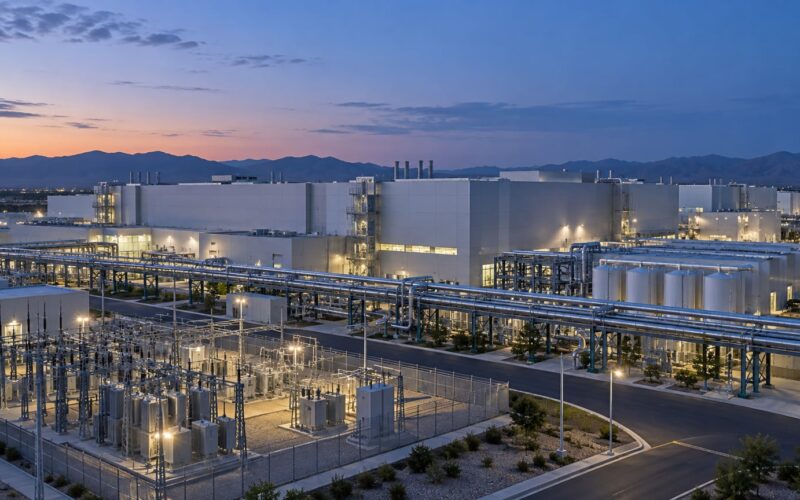
Contamination control in a semiconductor fab is the coordinated set of engineering and operational measures — cleanroom design, ultra-high-purity chemical and gas delivery, particle-controlled process equipment, disciplined personnel and material handling, wafer cleaning, and continuous monitoring — that keeps foreign particles, metals, molecules, and ions off wafers and out of process chambers so yield and process stability hold.
That is the short version. The full answer is messier, and it is worth understanding, because the topic usually gets explained as a list of contaminants rather than as a system. How fabs handle contamination control is really a question about where contamination comes from, which layer of the facility stops it, and how anyone finds out when a layer has failed.
One widely cited estimate from semiconductor manufacturing research puts contamination at roughly 75% of yield loss in integrated circuit fabrication. The other number engineers carry around is the killer particle rule: a particle larger than about a quarter of the minimum feature linewidth can create a fatal defect in the finished device. Both numbers shrink in tolerance as nodes shrink and as 3D structures stack up.
Table of Contents
- How Fabs Handle Contamination Control Across the Process
- What Kinds of Contamination Can Damage a Wafer?
- Particle contamination
- Metallic contamination
- Organic and molecular contamination
- Ionic contamination
- How Do Cleanrooms Reduce Airborne Contamination?
- How Are Wafers, Chemicals, and Process Gases Controlled?
- How Do Semiconductor Tools Prevent Process Contamination?
- What Are the Main Contamination-Control Layers in a Fab?
- How Do Fabs Monitor Particles, Chemicals, and Metals?
- What Happens When a Contamination Excursion Is Detected?
- Frequently Asked Questions
- What is the difference between particle contamination and chemical contamination in a semiconductor fab?
- Does a wafer need a cleanroom every time it is handled during manufacturing?
- How can a fab determine the source of particles found on a processed wafer?
- Which tools are most important for detecting metallic contamination?
- How often should contamination monitoring limits and cleanroom procedures be reviewed?
- Conclusion
How Fabs Handle Contamination Control Across the Process
Four control families do most of the work, and they stack on top of each other so that no single failure reaches a wafer:
- Facility controls — the cleanroom envelope, filtration, airflow, pressure cascade, and zoning that keep airborne contamination from accumulating in the first place.
- Utility and material controls — the delivery of process gases, chemicals, and ultra-pure water at the specified purity, with traceability from supplier to delivery point.
- Equipment controls — tool design, chamber materials, preventive maintenance, and clean-up recipes that stop tools from becoming a contamination source.
- People and material controls — gowning, entry protocols, material-in procedures, and wafer handling rules that limit what crosses the cleanroom boundary.
Running underneath all four is monitoring, and above all of it sits incident response. The governing principle across every fab I have read documentation for is prevention over removal. Contamination that is stopped at the source costs nothing but discipline; the same contamination that reaches a wafer has to be found, cleaned, and re-qualified, and the wafer may already be scrap.
The monitoring side is worth being honest about. Particle counts in a fab are a lagging indicator. By the time an excursion alarm trend shows up, production lots have usually already been exposed, which is exactly why every fab puts far more engineering effort into prevention than into detection.
What Kinds of Contamination Can Damage a Wafer?
Industry teams classify contamination into four main categories — particles, metallic contamination, organic and molecular contamination, and ionic contamination — with electrostatic charge and bio-contamination handled as special cases on top. The categories matter because each one comes from a different place, shows up under a different measurement, and cannot be fixed by the same remedy.
Particle contamination
Solid particles include dust, skin flakes, fibers from garments, silicon shards, and wear debris from moving tool parts. They land on a wafer and either break a device outright or create a nucleation site that becomes a defect later. Sources run from people and the building itself to pumps, motors, and chamber components. Optical particle counters and wafer surface scanners catch them, and the killer particle rule defines when one becomes fatal.
Metallic contamination
Metals such as iron, copper, sodium, and potassium arrive from wetted materials, chamber parts, chemicals, and even the stainless steel of the plumbing. They matter because they diffuse into silicon and silicon dioxide, creating deep-level traps that degrade device lifetime, and because they cross-contaminate a batch: one wafer carrying metal can taint a whole cassette of 25 in a batch clean.
Organic and molecular contamination
Airborne molecular contamination — AMC in industry shorthand — is the hardest class to catch. It includes outgassing from polymers, adhesives, paints, and building materials, plus solvents, pump oils, and skin-derived hydrocarbons. Individual molecules are far too small to see on a wafer, but they adsorb onto surfaces, shift etch rates, poison catalytic surfaces, and skew optical and electrical measurements. Fabs track it with dedicated chemical sensors and periodic surface analysis rather than with particle counters.
Ionic contamination
Mobile ions — usually alkalis such as sodium and potassium — come from wet processing steps, rinse water, glass and quartz components, and handling surfaces. On a thin dielectric they drift under an applied field, which is how a wafer that passed every particle check still produces out-of-spec devices. The classic detection is a surface potential or electrically induced oxide charge measurement.
| Type | Typical source | What it does to the process | How it is detected |
|---|---|---|---|
| Particle | People, building surfaces, tool wear, pump exhaust | Prints onto the wafer, blocks a pattern, seeds a later defect | Real-time particle counters, wafer surface scans, defect inspection |
| Metallic | Wetted parts, chamber components, chemicals, plumbing | Diffuses into films, creates deep-level traps, shortens device life | TXRF, VPD-ICP-MS, surface metal analysis, CV measurement |
| Organic and molecular | Outgassing from polymers and building materials, solvents, oils | Alters etch rates, poisons catalysts, shifts optical measurements | Chemical sensors, AMS headspace analysis, surface residue analysis |
| Ionic | Wet process steps, rinse water, glass and quartz parts | Drifts through thin dielectrics and shifts threshold voltage | Surface potential measurement, electrically induced charge testing |
| Electrostatic charge | Insulating surfaces, wafer handling, triboelectric effect | Attracts particles and can damage thin dielectrics | Ionization monitoring, charge-to-oxide test structures |
How Do Cleanrooms Reduce Airborne Contamination?
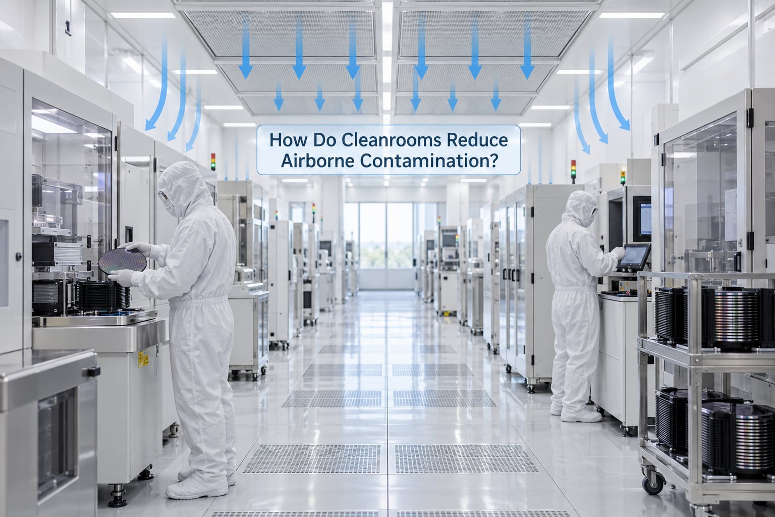
A cleanroom does not clean the air. It removes particles from the air at a controlled rate and then keeps new ones out, which means airflow design matters more than filter efficiency. Filters are only useful if the air actually flows through them.
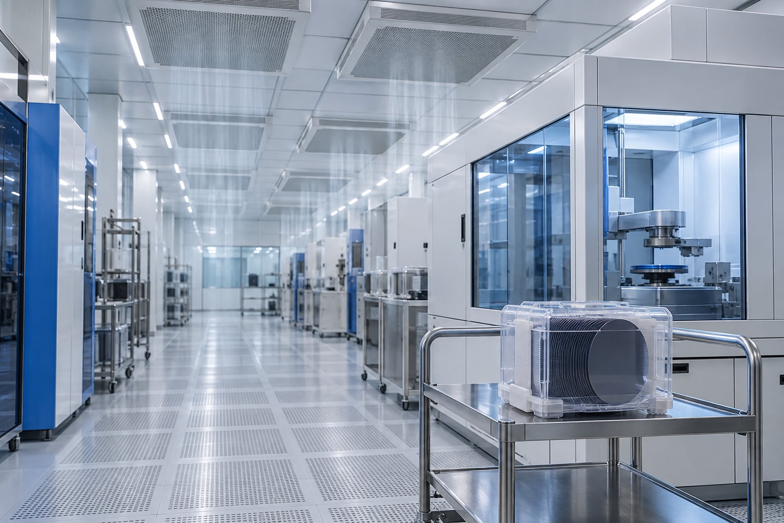
Three ideas do the work. First, unidirectional airflow: air moves in a single vertical path from the ceiling filter units down across the work area, sweeping particles away from the critical zone instead of swirling them through it. Second, the pressure cascade: each room sits at a slightly higher pressure than the one outside it, so air flows outward and contaminated air is never drawn into a cleaner space. Third, controlled entry: air showers, pass boxes, and gowned personnel entering through a controlled sequence rather than walking in from a corridor.
Classification comes from ISO 14644. The standard counts particles at and above 0.5 micrometres and defines a maximum concentration for each class: an ISO Class 5 room is allowed up to 3,520 particles per cubic metre at that size, while an ISO Class 1 space — used as a mini-environment around a lithography scanner — is limited to 10 particles per cubic metre down at 0.1 micrometres.
That gap is the real story. Most fab production areas run around ISO Class 5 to ISO Class 8 depending on the step, and the tightest conditions are created locally, as sealed mini-environments over the tool, inside the process chamber, or under a lithography canopy. The whole surrounding area then only has to protect the mini-environment rather than run at the same standard everywhere.
One more design detail catches people out: the materials in the room itself. A cleanroom full of low-shedding materials — no untreated plywood, no PVC, limited adhesives, no wall covering that flakes — is part of the control scheme, because a room can be filtered and still outgas onto the wafers.
How Are Wafers, Chemicals, and Process Gases Controlled?
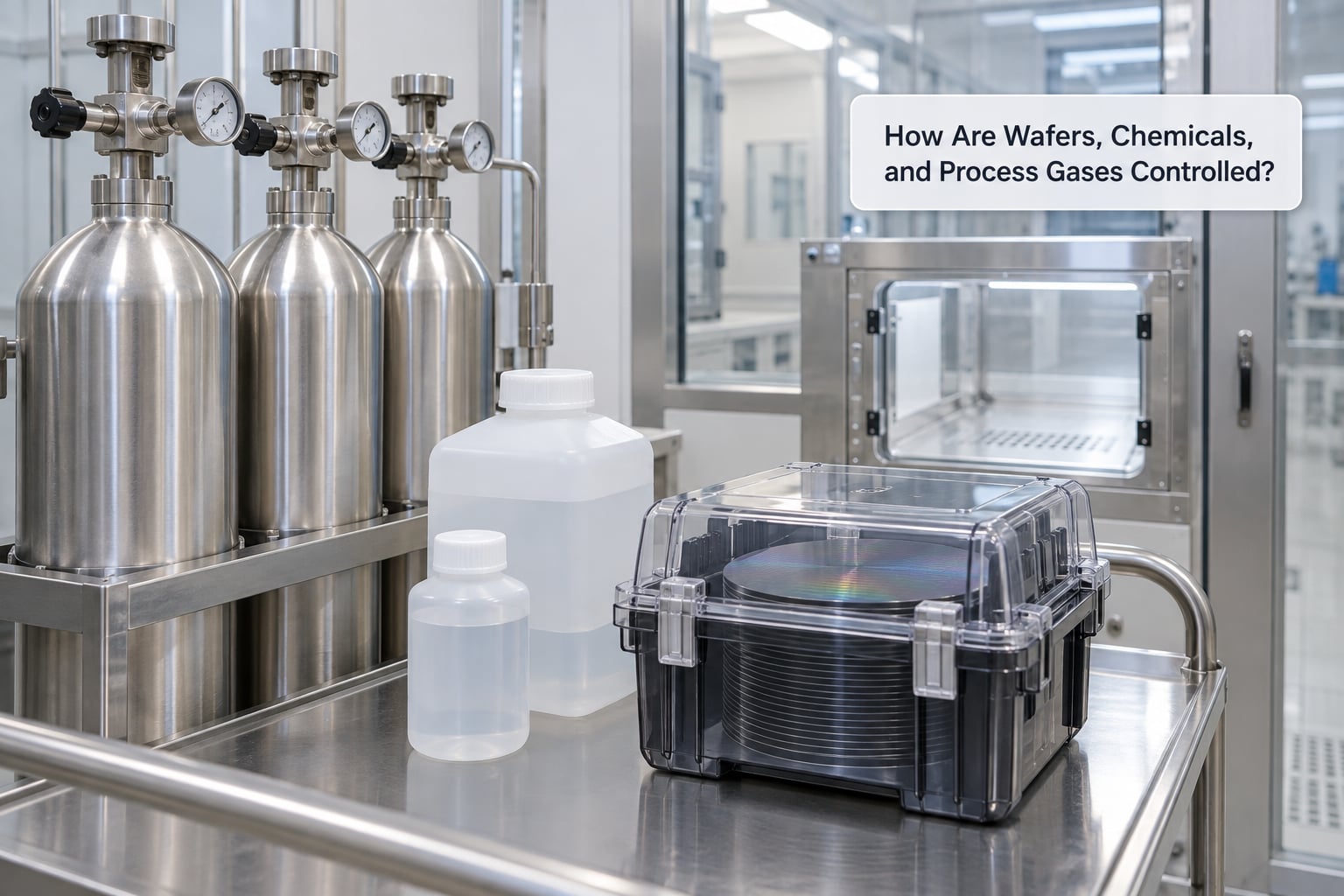
Clean air does nothing for contamination that arrives in a gas bottle or a chemical drum. Everything entering a process has to meet a written specification before it is allowed into the tool, and the delivery system has to get it there without adding anything of its own.
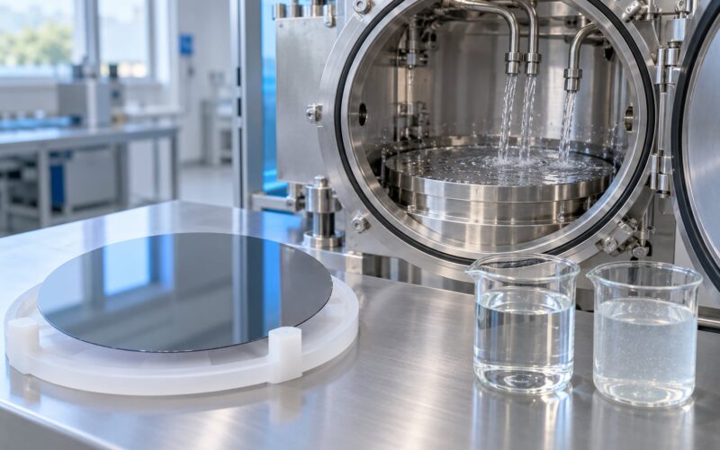
Wafers travel in sealed FOUP pods with filtered lids that keep particles off the surface between steps, get cleaned in wet clean steps between process layers, and are stored in controlled cabinets. Cleaning chemistry is where the last-line defence lives: SC-1 removes organic residue, SC-2 removes metal contamination, dilute hydrofluoric acid strips the native oxide, and ozonated deionized water is used for a final rinse. Batch tools immerse 25 wafers at a time, which is fast but carries the batch loading effect — as contaminants come off one wafer into the bath, later wafers in the same cassette pick them up. Single-wafer spray tools trade throughput for a much tighter per-wafer control, which is why they took over in advanced nodes.
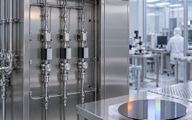
Process gases arrive at a specified purity and are delivered through electropolished stainless piping with minimized dead legs, so there is no stagnant volume where moisture and oxygen can sit and diffuse back into the gas. Systems are purged, pressure-tested, and leak-checked before use, and a gas cabinet outside the cleanroom supplies each tool through a controlled delivery system.
Bulk chemicals follow the same logic at larger scale. Stainless or fluoropolymer-lined delivery, dedicated lines per chemistry to avoid cross-contamination, and inline filtration with filter integrity testing all sit between the supply point and the tool.
Traceability closes the loop. Each container is linked to its lot, its supplier analysis, and the tool and process step where it was used, which is what makes a root-cause investigation possible when an excursion appears weeks later.
How Do Semiconductor Tools Prevent Process Contamination?
A process tool is a contamination source with a recipe. Chamber surfaces, wetted parts, seals, pumping lines, and the robot handling wafers inside the tool all shed, outgas, or accumulate material, and the tool has to be designed and maintained so that this happens slowly and predictably.
Materials of construction matter more than people expect. Chamber liners are chosen for low particle generation and low outgassing, wetted parts are made from materials that do not leach metals into wet chemistry, and elastomer seals are treated as a controlled life item because they age, outgas, and shed. Anything with a moving part is a wear point, and every wear point is a scheduled replacement rather than a failure waiting to happen.
Preventive maintenance is therefore part of contamination control, not just equipment reliability. Pumps get changed on a fixed interval instead of when they fail, chambers get cleaned on a defined schedule, and clean-up recipes — in-situ chamber cleans and the equivalent for wet tools — run on a known frequency. The chamber condition data from all of it feeds a trend, so a gradual increase in particle counts or chamber pressure signals a problem while the tool is still within specification.
Between products, tools run qualification: an empty chamber check, sometimes a wafer-based check. Practitioners refer to these as particle check quals, and they are run routinely on the tool level, with FOUP-based checks used to confirm that a carrier or a specific set of handling parts is not introducing particles before production lots are exposed.
What Are the Main Contamination-Control Layers in a Fab?
Here is the whole program in one view — what each layer controls, and how it typically fails in practice.
| Control layer | What it controls | How it typically fails |
|---|---|---|
| Facility and cleanroom | Airborne particles, airflow, pressure direction | Door left open, filter load too high, pressure cascade broken, construction dust inside the envelope |
| Utilities and materials | Gas and chemical purity, water quality, trace metals | Dead leg in the piping, a leaking seal, a depleted purifier, a chemical lot outside specification |
| Process equipment | Particles and films generated inside the tool | Worn seal, exhausted chamber liner, overdue PM, residue built up between cleans |
| People and material handling | Anything crossing the cleanroom boundary | Bad gowning, unwrapped material on a cart, contact with a bare wafer surface, tool-to-tool transfer residue |
| Wafer cleaning | Residue left on the surface before the next step | Batch loading effect, chemistry drift, incomplete rinse, pattern damage from over-aggressive clean |
| Monitoring and response | Turning an unseen problem into a bounded one | Alarm limits set too loose, sampling too sparse, excursion contained but never root-caused |
Read as a sequence, the layers describe the operating order a fab follows: design the environment, qualify the materials and equipment, monitor process conditions, investigate excursions, contain failures, and restore a verified state before production resumes.
How Do Fabs Monitor Particles, Chemicals, and Metals?
No single instrument covers this, so fabs run a stack of them and look at the trends rather than the absolutes.
Particle counters sit in the cleanroom air, in the tool exhaust, and inside process chambers, in some cases at sub-20 nm sensitivity as nodes shrank the sizes that matter. Wafer surface particle checks confirm that a specific carrier or handling path is not adding particles. Real-time counters are fast but tell you about the room; they do not tell you which lot was exposed.
Chemical and metal analysis works on samples rather than in real time. Surface metal analysis, total reflection X-ray fluorescence, or inductively coupled plasma mass spectrometry on an extracted surface give a quantitative read on metallic contamination. For molecular contamination, headspace analysis and chemical sensors track organic outgassing and specific gas species.
Electrical and process data is where contamination shows up as a business outcome: threshold voltage distributions, leakage current, sheet resistance, etch rate, and defect density per wafer. This is why defect sampling on its own is not enough. A sampling plan catches what it samples and stays silent about the rest, which is why fabs pair limited defect inspection with continuous process KPIs and long-term trend analysis.
The honest limitation is timing. Monitoring tells you a problem exists after the exposure has happened, so it bounds the damage and drives prevention rather than preventing the damage itself.
What Happens When a Contamination Excursion Is Detected?
Excursions are procedure-driven, and the sequence below is the industry-standard shape of the response rather than any one company’s proprietary method.
- Contain the lot. Stop and identify every lot that ran on the affected tool, in the affected process step, inside the exposure window defined by the last known-good check. Quarantine the material before the count grows.
- Preserve the evidence. Hold the suspect carriers, the gas or chemical delivery records, the tool sensor data, and the wafers themselves. A wafer that has already been cleaned tells you very little.
- Narrow the source. Work backwards through the tool: which part, which recipe step, which consumable, which PM was done most recently. Compare the tool’s data against its siblings on the same process.
- Assess the risk. Use the process window to decide whether the exposure could have moved a device parameter. That decision determines whether the lot can be reworked, downgraded to a less demanding product, or scrapped.
- Correct and clean. Change the part, the recipe, the seal set, the chemical lot, or the maintenance interval, then run the appropriate clean.
- Requalify before resuming. Re-run tool qualification and particle check quals, confirm the data sits back inside limits for a defined period, and only then return the tool to production.
- Document and prevent recurrence. Close the investigation with a written root cause, a corrective action, and a specific change to a specification, limit, or procedure so the next occurrence is caught earlier or does not happen at all.
Step seven is the one that gets skipped under production pressure, and it is the reason the same excursion shows up twice.
Frequently Asked Questions
What is the difference between particle contamination and chemical contamination in a semiconductor fab?
Particle contamination is solid matter, such as dust, fibers, or tool wear debris, that sits on a wafer and can block or distort a pattern. Chemical contamination is dissolved or adsorbed matter, including metals, ions, and molecular residues, that alters process chemistry and device electrical behavior rather than printing on the wafer. The two are detected with different tools, traced to different sources, and cleaned with different methods.
Does a wafer need a cleanroom every time it is handled during manufacturing?
Not the whole facility, no. Wafer handling happens in cleanroom areas matched to the process step, and the tightest conditions are created locally, as sealed FOUP pods, filtered-handling mini-environments, or the sealed chamber of the tool itself. A wafer that stays inside a closed pod between steps can move through a less stringent area than a wafer being manually loaded into an open process bay.
How can a fab determine the source of particles found on a processed wafer?
Start with containment. The fab identifies every lot that ran on the suspect tool inside the exposure window, then works backwards from the tool: chamber parts, wetted components, seals, the robot and end-effector, consumables, and the most recent maintenance. Air particle data, tool sensor trends, and comparison with sibling tools narrow it down, and a physical inspection of the wafer and its carrier often shows whether the particles are clustered in a pattern that points to handling or to a specific process chamber.
Which tools are most important for detecting metallic contamination?
The main techniques are total reflection X-ray fluorescence for rapid surface metal screening, and VPD or solution-based extraction followed by ICP-MS for a quantitative, low-detection-limit result. Fabs also use electrically biased structures, such as capacitor and charge-to-oxide test devices, because metal contamination shows up electrically long before it is visible on a wafer. Surface metal analysis is sampled rather than continuous, so it complements in-line monitoring.
How often should contamination monitoring limits and cleanroom procedures be reviewed?
At minimum on a defined schedule, typically annually, and immediately whenever something changes. A new process step, a new tool or supplier, a facility modification, a construction project, or a shift to a smaller node all change the risk profile and should trigger a review of ISO 14644 classification, alarm limits, and gowning and material-in procedures. Classified cleanroom areas are reclassified to ISO 14644-1 at planned intervals and after any work that disturbs the envelope.
For reference, the standards behind most of this are ISO 14644-1 for cleanroom classification and ISO 14644-3 for test procedure, the SEMI S-series for materials and safety in semiconductor manufacturing, and the IEST-RP-CC series of recommended practices for cleanroom design and operation.
Conclusion
How fabs handle contamination control is not a single system. It is a stack of independent safeguards — facility, utilities, equipment, people, cleaning, monitoring — designed so that any one of them can fail without a wafer being lost, and verified continuously so that the failure is found quickly.
Start by mapping your own operation. List the contaminant sources, mark the control point that catches each one, write down the monitoring limits that tell you a layer has failed, and document the escalation path. That map is the difference between a contamination program and a hope.