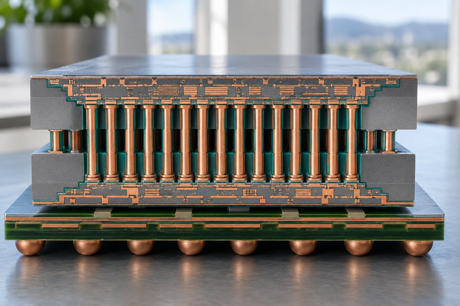
A through-silicon via (TSV) is a vertical electrical connection that passes completely through a silicon wafer or die, so that circuits on the front face can talk to circuits on the back face without routing a wire around the edge. The hole is lined with an insulating dielectric, sealed with a barrier layer, and filled with copper, and it is the structure that makes three-dimensional chip stacking practical. Most engineers meet TSVs first in high-bandwidth memory, but the same idea shows up in image sensors, stacked DRAM, silicon interposers and chiplet packages.
Think of a chip as a city with horizontal roads. Transistors sit at the intersections, and metal layers run power and data sideways through the silicon. When two chips need to talk to each other, a horizontal road is a long, slow detour that also burns power. A TSV is a vertical tunnel punched straight down through the city, so the trip from one layer to the next takes micrometres instead of millimetres.
Here is what this guide covers, in the order the questions usually arrive: what a via is physically, why stacking beats shrinking, how the structure behaves electrically, how a fab actually makes one, which variants exist, what breaks, and which interconnect method to pick when you are choosing a package.
Key takeaways
- A TSV is a copper-filled vertical channel through silicon, electrically isolated from the surrounding substrate by a dielectric liner.
- It shortens the path between stacked dies from millimetres of bond wire or interposer trace to tens of micrometres of vertical metal.
- Vias are classified by where they are formed in the process flow: via-first, via-middle or via-last.
- Filling, wafer thinning, alignment and known-good-die testing are the hard parts, not the copper itself.
- TSVs carry signals and power well, but they are not a heat pipe; a vertical metal column is a poor thermal path compared with a spreader.
- TSV and PCB via share a name and almost nothing else, which confuses a lot of searches.
Table of Contents
- What Are Through Silicon Vias?
- Why Through Silicon Vias Matter for 3D Chips
- How the Through Silicon Via Structure Works
- How Through Silicon Vias Are Fabricated
- Through Silicon Vias Explained Step by Step
- The through silicon vias explained flow, step by step
- Defining the via and its keep-out zone
- Forming a deep opening
- Insulating the sidewalls
- Filling the via
- Connecting the metal layers
- Testing electrical continuity
- What Are the Main Types of Through Silicon Vias?
- What Electrical and Thermal Benefits Do TSVs Provide?
- What Challenges Do Through Silicon Vias Create?
- How Do TSVs Compare with Other 3D Interconnect Methods?
- TSV vs PCB via: why the names collide
- Where Are Through Silicon Vias Used?
- What Design Considerations Matter for TSV Integration?
- Frequently Asked Questions
- What is a through-silicon via (TSV)?
- What are vias in semiconductors?
- What is the difference between a TSV and wire bonding?
- How many layers can you stack with TSVs?
- Do TSVs carry heat away from stacked dies?
- What is a TSV used for?
- Conclusion: Start With the TSV’s Connection Path
What Are Through Silicon Vias?
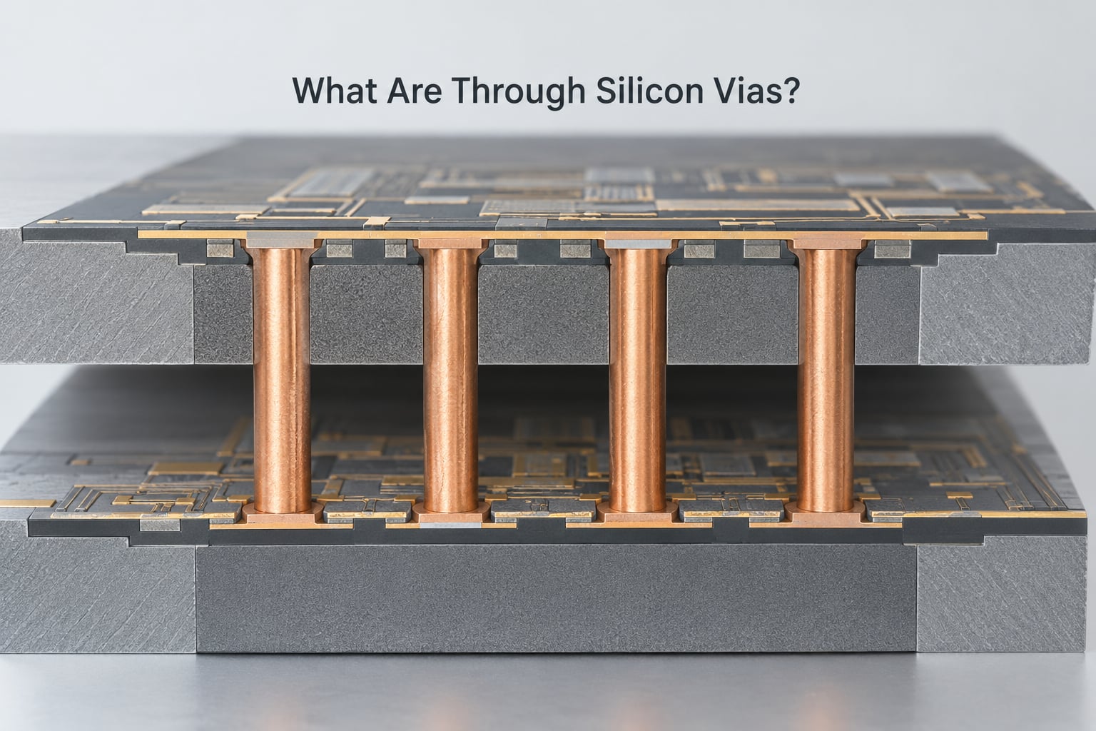
A through-silicon via is a vertical conductive plug that runs from one face of a silicon wafer or die to the other, carrying power, ground and data between the circuitry on those two faces. In practice the conductor is electroplated copper, the insulator is a deposited oxide or polymer liner, and a thin barrier such as tantalum or titanium prevents copper from diffusing into silicon. Where a via stops short of the far side, it is not a through-silicon via at all; those are called blind or buried vias, and they are the board-level terms that leak into chip conversations.
The distinguishing feature versus other chip interconnects is direction. Wire bonds and flip-chip solder bumps are surface features: they sit on the top of a die and reach sideways to a neighbour. A TSV goes through the body of the die, which is why the back face has to be thinned until the copper is exposed. That thinning step is also why TSV die ends up thinner than a conventional die.
A second distinction worth stating early, because search results constantly blur it: a TSV is not a PCB through-hole. The names match, the physics does not. A board via is a plated hole in a laminate board, tens of micrometres across, drilled by a mechanical bit. A TSV is formed by etching solid silicon to a much tighter pitch, lined, seeded and filled in wafer-level processes, then used to stack active dies.
Why Through Silicon Vias Matter for 3D Chips
TSVs matter because planar scaling stopped paying for itself, and going vertical keeps performance climbing without depending on another transistor shrink. A lithography reticle, a mask that defines a whole die, has a hard size ceiling of roughly 850 square millimetres, so a large processor has to be split into chiplets rather than drawn as one giant die. Splitting a design means adding interconnect, and interconnect delay has been the stubborn part of scaling for decades: wires get longer relative to the gates they connect, resistance rises, signal integrity degrades, and every transition burns power.
A TSV turns that horizontal problem into a short vertical one. In a stacked die the connection between two layers is measured in tens of micrometres of metal rather than millimetres of wire loop or a centimetre-long trace across a silicon interposer. Shorter paths mean lower resistance, lower capacitance, less delay, and lower energy per bit moved, which matters most for the power-hungry transfers that dominate memory traffic.
There is a second, subtler reason stacking is attractive, and it comes from geometry rather than electricity. Once a die is thinned enough to be stacked, a package can be made from many thin layers occupying the same footprint as one thick one. Stack height then buys density that the reticle limit would otherwise deny you. High-bandwidth memory is the clearest case: threads discussing HBM roadmaps describe the mechanism as cutting individual DRAM die thickness by roughly 40 percent so more layers fit the same stack height, and that thinning is only possible because the vias survive it.
Heterogeneous integration follows the same logic. If the via channel works, you can place logic, memory and analog blocks made on different process nodes in one package, and let each node do what it is best at. That is the argument behind chiplets in general and behind 3D cache stacking in particular.
How the Through Silicon Via Structure Works
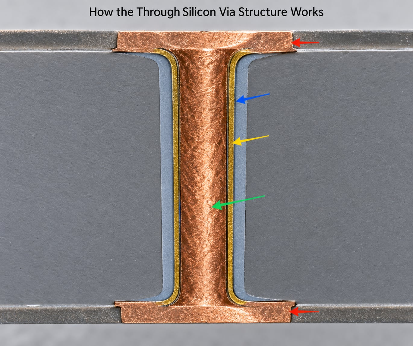
A TSV is built in concentric layers, and each one has a job. At the centre is the conductor, almost always copper. Around it sits a barrier and seed layer a few tens of nanometres thick, whose purpose is to stop copper atoms from migrating into the silicon and to give the electroplating process a surface that grows evenly. Outside that is the dielectric liner, typically a deposited oxide, which is what actually electrically isolates the via from the substrate. Without the liner the via would short to the surrounding silicon, because doped silicon is a conductor, not an insulator.
At each end of the via sits a landing pad, a wider metal feature that the via plugs into. The pad is what gets bonded to a neighbouring die, and its job is to spread current and to give the bonding process a flat, uniform surface. Without it, current would concentrate at the narrow via and any misalignment during bonding would create an open circuit.
Two geometry terms describe every via. Pitch is the edge-to-edge spacing of adjacent interconnects, which is the trace width plus the space between traces, not the centre-to-centre distance; the distinction matters when you compare a TSV pitch to a bump pitch. Aspect ratio is the via depth divided by its diameter, and it is the number that decides whether the fill will succeed. Copper plating into a narrow, deep hole is hard, and the practical ceiling sits somewhere around 20:1. Push past that and you get voids and seams that show up later as open or resistive vias.
Electrically, a TSV is not a wire. It is a short transmission line with resistance on the order of tens of milliohms, a capacitance measured in femtofarads, and a small inductance. The capacitance is what creates coupling: a fast signal switching in one via pushes charge into its neighbours and shows up as noise on the quiet ones. That is why the area immediately around a via, the keep-out zone, is usually ringed by a grounded guard structure or filled with dummy metal, both to contain the coupling and to keep mechanical stress away from sensitive devices.
How Through Silicon Vias Are Fabricated
A TSV is made in a fixed order, and each step exists to make the next one possible. The sequence below is the common front-end style for copper vias, in the order an engineer would describe it.
- Define and etch the opening. A lithography mask opens the via footprint and deep reactive-ion etching (DRIE) cuts the hole straight down. The Bosch process is the standard DRIE variant, cycling an etch step and a polymer passivation step so the sidewalls stay vertical instead of tapering.
- Line the walls with a dielectric. A conformal oxide or polymer deposition coats the sidewall and the bottom, electrically isolating the via from the substrate. Scallops left by the Bosch process must be smoothed here, because a rough sidewall is a void waiting to happen during plating.
- Deposit the barrier and seed. A thin refractory barrier is laid down by physical vapour deposition, then a copper seed by sputtering or deposition. Without a continuous seed, electroplating nucleates unevenly and the fill is full of voids.
- Fill the via with copper. Electrochemical deposition grows copper from the seed until the via is closed, often with a cap and a plating bath additive to suppress dishing. This is the step that sets the aspect-ratio limit in practice.
- Planarize. Chemical mechanical planarization (CMP) removes the copper overburden and leaves a flat surface so the next metal layer can be deposited on top.
- Thin the wafer from the back. The wafer is ground and polished from the backside until the buried copper is exposed, and the remaining silicon is often recessed further to let the stack sit down. The dielectric on the back surface is opened to reach the via.
- Build pads and the redistribution layer. Redistribution metal on the front, backside, or both lands on the exposed copper, and the die is ready to be bonded to another die or to a carrier.
Everything after the fill is mechanical and thermal work, and it is where most of the process risk lives. Etching a hole is comparatively forgiving; thinning a wafer until it is a few tens of micrometres thick, and then handling it, is not.
Through Silicon Vias Explained Step by Step
The through silicon vias explained flow, step by step
Here is the same sequence walked through as one via’s life story, from a mask rectangle to a tested connection, so the order is unambiguous when you are reading a process flow or talking to a packaging house.
Defining the via and its keep-out zone
The via is drawn in metal layout like any other feature, with its own design rules for diameter, pitch and spacing. Around it the designer places a keep-out zone, a region where no sensitive devices sit, because the copper and silicon expand at different rates and the stress that creates can shift device thresholds.
Forming a deep opening
DRIE bores the hole in a single pass, switching repeatedly between etch and passivation chemistries to hold the sidewall. The result is a high-aspect-ratio hole with a flat bottom, which is exactly what the next steps need.
Insulating the sidewalls
The liner deposition coats the full inner surface. Its thickness has to be uniform from the top of the via to the bottom, because thin spots are where leakage starts, and it has to be smooth because rough silicon is where copper cracks appear under thermal cycling.
Filling the via
Copper plating closes the hole from the bottom up. Trapped chemistry and gas are the enemy here, and any void left behind is a site for electromigration damage years later, which is why via fill quality shows up so often in reliability failure analysis.
Connecting the metal layers
After CMP and backside thinning, pads and redistribution layers tie the via into the local interconnect on both faces. Redistribution layers exist because the vias are on a coarse pitch while the circuitry above them is on a much finer one, and something has to fan the connections out.
Testing electrical continuity
Before dies are stacked, each die is probed and screened so that only known-good die goes into a stack. This matters more than any other step, because in a stack of n layers the probability that every layer is good is the product of the individual yields, and that number falls fast. The reason most stacked designs ship in high volume is aggressive test coverage and thinning to remove known defects before bonding, not a sudden improvement in front-end yield.
What Are the Main Types of Through Silicon Vias?
TSVs are classified by where they are formed relative to the front end of line, where transistors are built, and the back end of line, where the interconnect stack is built. The choice sets the thermal and stress budget the process can tolerate, so it is decided early.
| Type | Formed when | Main trade-off | Typical use |
|---|---|---|---|
| Via-first | Before the front end of line, sometimes before the transistors exist | Lowest density, and the via must survive every later high-temperature step; not compatible with modern aggressive anneals without special materials | Older logic processes, image sensors, MEMS |
| Via-middle | Between front end of line and the back end interconnect stack | A balanced point: the silicon is finished but still thick enough for wafer handling, and standard BEOL temperatures are fine | High-bandwidth memory, stacked DRAM, CMOS image sensors, most high-volume 3D work |
| Via-last | After the back end of line, in the packaging flow | Full access to a finished wafer and the best compatibility with fine logic processes, but the backside has to be reached and finished after the fact | Logic-on-logic stacking, chiplets, advanced foundry 3D offerings |
Length is the second axis. A through-wafer via passes from face to face and requires full backside thinning. A blind via stops at an internal landing layer and is opened from one side only, typically a redistribution layer. A buried via is stopped and buried inside the stack, opened on neither face. Through-wafer vias are what people usually mean by TSV; blind and buried vias are the same geometry vocabulary borrowed from printed circuit boards.
What Electrical and Thermal Benefits Do TSVs Provide?
The electrical benefits come down to short, dense, low-loss paths. Reducing the connection between dies from millimetres to tens of micrometres cuts both resistance and capacitance, which lowers propagation delay and, more importantly, lowers the energy spent charging and discharging that capacitance on every transition.
- Lower delay. The interconnect no longer dominates the critical path, which is what lets logic designers spend their timing margin on real logic instead of on getting a signal across a package.
- Higher connection density. Vias are far denser than bond pads or solder bumps, which means more parallel signal lanes and more power pins in the same area.
- Cleaner signal integrity. Short paths mean less loss and less coupling, and the vertical geometry keeps lanes parallel rather than splaying out like bond wires do.
- Power delivery. A dense grid of vias drops supply voltage into the middle of a die, which matters for high-current designs where the on-die distribution network cannot carry current from the edge alone.
- Flat profile. Stacking removes the loop height of wire bonds, which is often the real constraint in a device thin enough to fit in a phone.
The thermal claim deserves a straight answer, because it is the one most often oversold. A filled copper via is a decent conductor in the vertical direction, and a dense array of them does conduct some heat from a thinned die. It is not a solution to the thermal problem, and it does not replace a heat spreader. Stacking concentrates power in a smaller volume, and the heat still has to leave through the package, substrate and board. Treat via-based heat conduction as a secondary benefit and size the real thermal path separately.
What Challenges Do Through Silicon Vias Create?
TSVs trade a planar problem for a set of harder ones, and none of them are solved by better copper.
Fill and void formation. Plating a narrow, deep hole without leaving voids is the core process challenge, and voids become open circuits or high-resistance sites after thousands of thermal cycles. Aspect ratio is the main lever, which is why fine-pitch designs push harder on alternative fills such as tungsten or direct bonding.
Wafer thinning and handling. A die that ends up tens of micrometres thick is fragile. Backside grinding, temporary bonding to a carrier, and the final debond all add handling risk, and a scratch at that stage can scrap a die that was perfectly good.
Alignment. Two dies bonded together must line their vias up to a fraction of the pitch. A misplaced bond turns a connection into an open circuit, and at 5 micrometre pitch the tolerance budget is unforgiving.
Yield multiplication. If a die has a 95 percent chance of containing a working via field, a stack of ten such layers is at about 60 percent overall before any other failure modes. This is why known-good-die screening, repair redundancy and design-for-test matter more in 3D than in 2D, and why vendors quote stack heights in terms of what they can test rather than what they can build.
Parasitics and coupling. Every via brings capacitance to the node it touches, and a dense field brings with it crosstalk from its neighbours. Design rules on spacing, shielding and keep-out zones exist to bound this.
Thermomechanical stress. Silicon expands at roughly 2.6 parts per million per degree Celsius and copper at about 16.5, so a filled via is a bimetallic column pulling against its own liner every time the package heats or cools. That stress shows up as shifted transistor thresholds, via resistance drift, and eventually as delamination. Copper’s lower expansion is one reason tungsten fills and lower-expansion composites are studied for deep and high-reliability cases.
Electromigration. Current density in a via is high because the cross-section is small, and copper atoms drift along the electron flow. Over enough time and current, a void forms and the connection degrades. Design rules that limit current per via, redundant parallel paths and better barrier materials all push this back.
Inspection. A void inside a filled via is not visible from the surface. Electrical test finds it after the fact; finding it during manufacturing needs X-ray or acoustic methods, which are slow and hard to resolve on fine pitches.
How Do TSVs Compare with Other 3D Interconnect Methods?
TSVs are the vertical channel; the methods below decide how two dies are brought together and how fine the connection pattern can be. Comparing them on pitch and path length tells you most of what matters.
| Method | Typical pitch | Connection density | Connection length | Main process demand |
|---|---|---|---|---|
| Wire bond | Tens of microns, pad-limited | Low, a few hundred per mm² | Millimetres of loop | Low cost, low density, tall profile |
| Flip-chip with microbump or copper pillar | About 40 to 100 microns | Several hundred to roughly 1,600 per mm² | Microns, very short | Reflow or thermal compression bonding, underfill |
| Hybrid or direct bonding | Single-digit microns possible | Tens of thousands per mm² | Microns, shortest | Extremely flat, particle-free surfaces; anneal |
| Silicon interposer with TSVs (2.5D) | Interposer TSV pitch set by the interposer process | High on the interposer, but routing length grows | Millimetres of horizontal trace, plus the via | Large interposer, extra wafer cost, reticle stitching |
The practical split: microbumps still carry most shipping volume because they are cheap and well understood, while hybrid bonding is where the density is heading. AMD’s stacked cache design in Zen 3 is the reference point most people cite, bonding at a pitch of roughly 9 micrometres and paying a small latency penalty for the extra hop in exchange for a large cache capacity gain. Intel’s Ponte Vecchio combined 47 chiplets on 2.5D with Foveros 3D stacking at a pitch around 36 micrometres, and Samsung’s 3D X-Cube and TSMC’s SoIC are the same idea in different process flows.
TSV vs PCB via: why the names collide
Searches for this topic keep landing on board-via answers, so here is the disambiguation in one table. They share a three-letter acronym and nothing else that a chip engineer would recognise.
| Attribute | Through-silicon via | PCB via |
|---|---|---|
| Substrate | Single-crystal silicon die or wafer | Glass-fibre laminate printed circuit board |
| How the hole is made | Deep reactive-ion etching of solid silicon | Mechanical drilling or laser ablation |
| Typical diameter | Around 1 to 10 micrometres | Tens to hundreds of micrometres |
| Wall treatment | Dielectric liner, barrier, seed, copper fill | Plated barrel, usually no dielectric liner |
| Electrical job | Signal, power and ground between stacked dies | Signal and power routing between board layers |
| Where it lives | Inside the semiconductor package | Inside the circuit board |
Where Are Through Silicon Vias Used?
TSVs ship in high volume in a handful of products, and the honest answer is that logic-on-logic stacking is the newest of them, not the most established.
High-bandwidth memory. HBM is the reason most people have heard of TSVs. Stacked DRAM dies are thinned, thinned again if necessary, and connected by a dense via array to a base die that handles the interface. JEDEC’s Wide I/O standard (JESD229) exists because the wide parallel interface that makes HBM fast needs exactly this many short connections.
Stacked DRAM and wide I/O mobile memory. The same vertical stack gives mobile DRAM more bandwidth in a narrow package outline.
CMOS image sensors. Sensors stack a logic die under or over the pixel array, which is how backside illumination works. Thinning the silicon lets light reach the photodiodes directly instead of passing through circuitry, and the connection between the two dies runs through vias.
Silicon interposers for 2.5D integration. Here the via array is in the interposer, not the compute die, and it carries signals between chiplets placed on its surface. This is the route taken by large AI accelerators and high-performance computing parts.
Logic-on-logic and cache stacking. AMD’s 3D V-Cache and Intel’s Foveros are the commercial examples. Practitioners generally describe this as the genuinely novel application, since the memory and sensor cases are mature and largely settled.
MEMS and sensor co-packaging. MEMS dies are often stacked with an ASIC beneath them, with vias passing data from the mechanical structure to the electronics.
Decoding the commercial names, since practitioners search for these more than for the generic term:
| Branded stack | Company | How it connects layers |
|---|---|---|
| 3D V-Cache | AMD | Hybrid bonding of a cache die onto a compute die, fine pitch |
| Foveros | Intel | TSV-bearing base die with microbumped die-on-die stacking |
| Co-EMIB / EMIB | Intel | Bridging die embedded in the package substrate for 2.5D links; bridges rather than a full stack |
| 3D X-Cube | Samsung | TSV-based die stacking with a face-to-face bonding option |
| SoIC | TSMC | Front-end-style bonding for very fine pitch logic stacking |
| FOCoS | ASE | Face-to-face chip-on-wafer stacking using TSV and copper pillars |
SK hynix and Micron are the other two HBM suppliers, and threads on r/SKHynix treat TSV capacity and substrate supply, not the logic die, as the tight steps in the supply chain. That is a fair summary of where the difficulty sits in the whole flow.
What Design Considerations Matter for TSV Integration?
The decisions that determine whether a TSV design works are made well before anyone picks an etcher, and they interact more than most checklists admit.
Pitch and diameter. Pitch is the edge-to-edge spacing of adjacent interconnects, and it is the number that caps connection density. Smaller pitch means more lanes in the same area, but it also means tighter coupling, harder plating and worse alignment tolerance.
Aspect ratio and fill metal. Depth over diameter decides which conductor you can use. Copper plates well to moderate ratios; deeper or narrower vias push people toward tungsten or other fills, with different resistance and different process steps.
Placement and keep-out. Vias have to land somewhere, and the region around each one is off-limits for sensitive circuitry. Under the array sits a thermal-mechanical stress field, so the floorplan, not just the router, is what determines where a TSV array can sit.
Power and thermal budget. A stack concentrates heat, so the thermal path has to be designed alongside the electrical one. The type choice, via-first through via-last, is fundamentally a thermal decision.
Signal integrity and timing. Via capacitance and neighbour coupling land in the timing analysis and in the power integrity analysis. Tools from Cadence and Ansys are commonly used for the electromagnetic and thermal simulation that tells you how much margin the arrangement leaves.
Test and redundancy. Decide early how each die is probed, what coverage you need, and what happens when a via is open. Repair structures, spare rows and partial redundancy all cost area that you will want back, so this is a yield decision as much as a test decision.
Mechanical support. Thin dies in tall stacks need something to carry load, which is why structural fill, dummy metal and dedicated fill dies appear in real designs. They also help the thinning step behave.
Frequently Asked Questions
What is a through-silicon via (TSV)?
A through-silicon via is a vertical electrical connection, usually a copper-filled channel lined with a dielectric and a barrier layer, that passes completely through a silicon wafer or die. It lets circuits on the front face connect to circuits on the back face, which is what makes it possible to stack dies and route power, ground and data straight up through the silicon instead of around its edge.
What are vias in semiconductors?
A via is simply a conductive path that connects two conductive layers in a chip. In the front end it links transistor layers. In the back end it links metal interconnect layers through a thin dielectric. A through-silicon via is the special case where that path runs from one face of the die to the other. PCB vias work the same way in a different material, which is why the terms get confused.
What is the difference between a TSV and wire bonding?
Wire bonding attaches dies side by side with thin gold or copper wires looped from a pad on one die to a pad on the other, giving millimetre-long paths and a tall profile. A TSV passes through the die and stacks dies face to face, giving micrometre-long vertical paths in a much flatter package. The trade is density and speed against yield, cost and thermal complexity.
How many layers can you stack with TSVs?
Products ship with up to sixteen or so DRAM layers in a single HBM stack, and logic stacks are smaller today, typically two to four active layers. The limit is not geometry but yield. Each added layer multiplies defect risk, so every extra tier needs known-good-die screening, repair structures and thinning to keep the stack testable.
Do TSVs carry heat away from stacked dies?
They carry some heat, since a dense array of copper columns conducts vertically, but a via is a poor thermal path compared with a spreader or heat sink. Stacking concentrates power in less volume, so the real thermal path still runs through the package, substrate and board. Treat via-based heat conduction as a secondary benefit and design the primary path separately.
What is a TSV used for?
TSVs are used to stack chips and move data between them. In practice that means high-bandwidth memory over a logic base die, stacked DRAM, CMOS image sensors with backside illumination, silicon interposers for 2.5D chiplet integration, cache-on-compute stacks for processors, and MEMS or sensor dies bonded to their ASICs. The unifying job is short, dense vertical interconnect.
Conclusion: Start With the TSV’s Connection Path
Everything about a through-silicon via reduces to one idea: a short, dense, vertical electrical path straight through the body of the silicon, so stacked dies can exchange data and power in micrometres rather than millimetres. If you take one mental model away, take that one, and be precise about the two terms that trip people up. Pitch is edge-to-edge spacing, and a TSV is not a PCB via.
Start by asking whether the design actually needs a vertical conductive path, or whether an interposer at 2.5D buys the same bandwidth with more forgiving process rules. Then work the four constraints in order: fabrication, since via-first, via-middle and via-last set the whole process budget; electrical, since aspect ratio, fill metal and coupling decide what the signal sees; thermal, since stacking concentrates heat and a via is not a heat pipe; and mechanical, since thinned dies, CTE mismatch and alignment decide what survives a temperature cycle. Where you land on that, the choice of bonding method and stack height follows fairly directly.