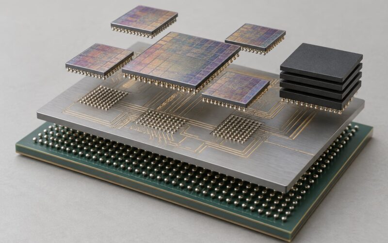
ESD protection in chip design means building circuits on the die itself, at the I/O bond pads and supply rails, that shunt a sudden electrostatic discharge pulse away from sensitive core circuitry and into a nearby rail before it can break down a thin gate oxide or latch the device. A good network does this in a few nanoseconds and stays invisible during normal operation.
The rest of this guide walks through what that pulse actually is, how it kills a transistor, which protection devices engineers reach for and why, the layout rules that decide whether a network works, and how to verify it before silicon.
Table of Contents
- Key Takeaways
- What Is ESD Protection in Chip Design?
- How ESD Damages an Integrated Circuit
- Which event are you designing against?
- Where Does ESD Protection Go on a Chip?
- How ESD Protection in Chip Design Differs by Signal Type
- How to Choose the Right ESD Protection Devices
- What Layout Rules Reduce ESD Risk?
- How Can Engineers Verify ESD Protection?
- What Common ESD Design Mistakes Should Be Avoided?
- Frequently Asked Questions
- What is the difference between ESD protection and surge protection?
- Should every chip pin have an ESD protection circuit?
- How low must the capacitance of an ESD protection device be?
- Why does ESD protection need a short ground return path?
- What should engineers do when a chip fails an HBM or CDM test?
- Conclusion
Key Takeaways
- ESD is a voltage problem, not a current problem. Damage comes from the field the pulse creates, so a fast clamp that holds the pad below the breakdown voltage saves the device even with kilovolt-class stress applied.
- The pulse is brutal in timing. A discharge reaches peak current in roughly 2 to 4 nanoseconds, which means protection has to be physically present at the pad, not a few millimeters away in the core.
- On-chip and system-level protection solve different problems. Die-level structures are qualified under JEDEC JS-001 and JS-002; board-level TVS diodes are qualified under IEC 61000-4-2. Most products need both.
- Every device trades something. Area, leakage, capacitance and clamp voltage are the four dials. You cannot turn all of them to the best setting at once.
- Some pads deliberately have no protection. Power switching nodes are the classic case, and there is a defensible reason for each omission.
What Is ESD Protection in Chip Design?
Electrostatic discharge is the sudden flow of charge between two objects at different potentials. Charge accumulates by triboelectric charging, which is the rubbing of two materials against each other. A person walking across a carpet, a plastic wafer carrier being separated from a wafer, or a PCB being slid off a bench all build up a potential in the kilovolt range without discharging visibly.
Air breaks down at a field strength of roughly 40 kV/cm under ordinary lab conditions. Humidity, temperature and pressure all move that number, which is why the same dry bench and a humid bench produce very different damage rates.
Integrated circuits are exposed at every place where the die meets the outside world. That means I/O pads, analog sensing pins, clock inputs, antenna feeds, and the exposed connections of any package that a customer can touch. On-chip ESD protection is the set of structures placed at those boundaries to intercept a discharge before it reaches the core.
The strategy in plain language is simple: give every externally reachable node a low-impedance escape route to a rail, close enough that the current never has to travel through functional circuitry, and make sure that route is off during normal operation.
Worth stating plainly for anyone new to the field: on-chip protection is not device shopping. Practitioners consistently say you cannot pick a clamp without understanding the victim circuit it protects, its voltage tolerance, and what it is allowed to do to the signal. The device is the last step of the design, not the first.
How ESD Damages an Integrated Circuit
Damage comes from local power dissipation. A discharge dumps energy into a region a few microns across, and the current density in that spot does the work.
Dielectric breakdown is the headline failure. Gate oxide fields approach 1 V/nm in scaled processes, and a pulse that pushes the field past the oxide’s breakdown strength punches a conductive path through the oxide. The transistor is now leaky or shorted, sometimes permanently, sometimes only above a temperature.
Junction damage shows up at pn junctions. Avalanche current heats a small spot, and the metal or the dopant profile at that spot degrades. These defects frequently pass the factory test and fail later in the field.
Latch-up happens when parasitic bipolar structures in the substrate or wells turn on. A conducting parasitic path from rail to rail dumps current until the device dies or requires a power cycle. Good ESD design keeps the substrate current path away from the well taps so this never starts.
Latent damage is the most expensive category. The part works at the test bench, degrades over months, and returns as an intermittent field failure that is nearly impossible to trace back to a handling event in assembly.
ESD accounts for a large share of semiconductor field failures, and the share grows with every node. As dimensions shrink, oxide dielectric strength and junction margins fall while the electrostatic stress applied by a person stays exactly the same. The tolerance band gets narrower every generation.
Which event are you designing against?
Three standardized models describe the stress. They are not interchangeable, and a design that passes one tells you nothing about the other two.
| Model | Source capacitance | Series resistance | Pulse rise time | What it simulates | Standard |
|---|---|---|---|---|---|
| Human body model (HBM) | 100 to 150 pF | 1.5 to 1.8 kOhm | Slow, microsecond-scale | A charged person touching a pin, or a charged assembly discharging into a grounded part | JEDEC JS-001 |
| Machine model (MM) | Zero, conductive source | Zero | Extremely fast, sub-nanosecond | A low-impedance production machine or grounded metal tool contacting a lead | JEDEC JS-001 |
| Charged device model (CDM) | Device capacitance, a few pF | Package inductance | Sub-nanosecond | The charged die itself discharging through a package pin during automated handling | JEDEC JS-002 |
Engineering relevance differs sharply. HBM and MM are slow enough that a decent clamp with a few ohms of dynamic resistance can respond in time. CDM is the hard one: a few picofarads discharging through package inductance produces a current spike with a rise time measured in fractions of a nanosecond, and the clamp has to be physically adjacent to the pad to be fast enough.
DigiKey forum contributors make a fair point that gets skipped in most write-ups: the name human body model is a misnomer. It represents discharge from any charged body, or a charged device, into an ESD-sensitive part. The numbers matter more than the label.
Where Does ESD Protection Go on a Chip?
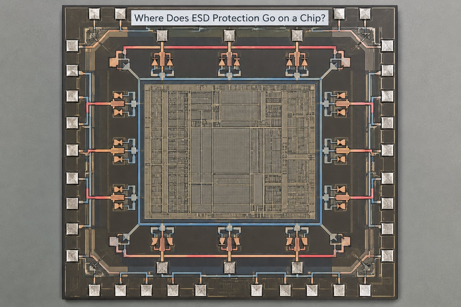
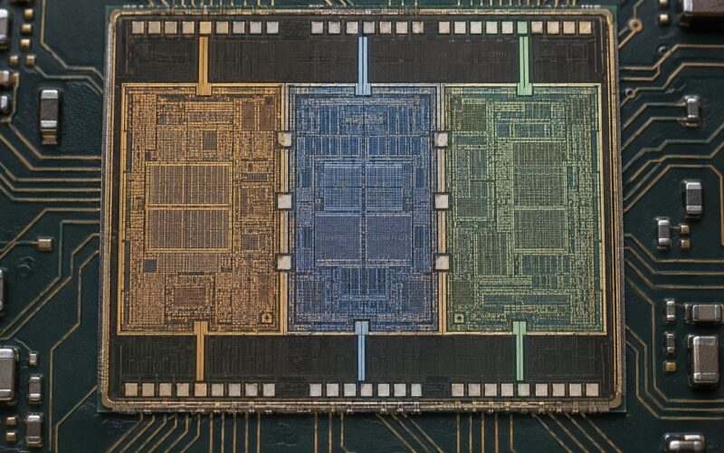
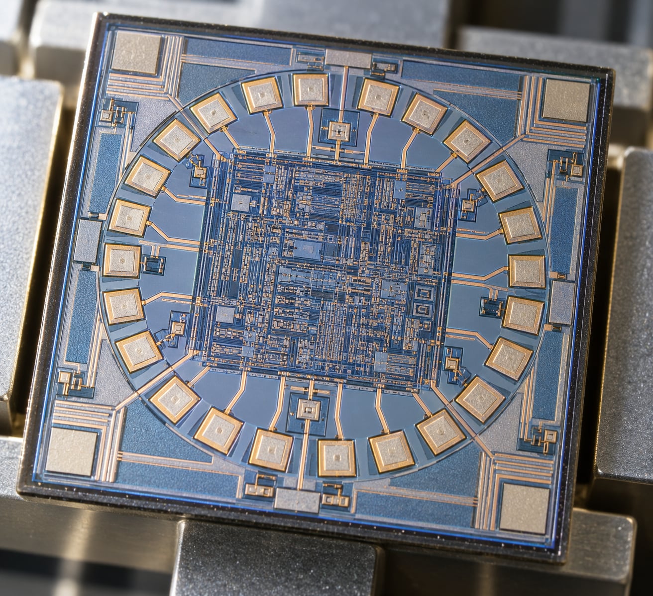
Protection lives in the pad ring, the ring of cells between the core and the bond pads. A pad cell usually contains the pad metal itself, the input buffer, an output driver, and a clamp structure tied to a supply rail or to ground.
At the die boundary there are really only a few categories of node, and each one gets a different answer.
Signal I/O pads get a clamp between the pad and a rail. For a positive-going excursion, current flows into the rail through a diode or an active clamp. For a negative excursion, a diode to ground handles it.
Supply rails get a rail-to-rail clamp, usually a stack of thick-field devices between VDD and VSS, rated to absorb the full discharge current. Rail clamps are what keep a pad from pumping energy into the core’s own supply network.
Analog sensing pins need low leakage more than anything else. A sensor input can sit at microvolt sensitivity, and a clamp that leaks tens of microamps is useless there regardless of how well it clamps.
High-speed interfaces are the capacitance problem. Every clamp adds junction capacitance to the node, and on a multi-gigabit link that capacitance fights the edge rate directly.
Exposed package connections such as a heat pad, a substrate ground, or an antenna feed are the awkward cases because the pad is mechanically large and often left floating by the integrator.
The important distinction for new designers is between the external clamp network and the circuitry it protects. The clamp’s job ends at the rail. What happens to the rail after that, whether the core supply can absorb the energy or whether the pulse appears across the core’s own decoupling, is a separate design problem that clamp selection does not solve for you.
How ESD Protection in Chip Design Differs by Signal Type
Digital inputs and outputs are the easiest case. The voltage tolerance is known, the edge rate is defined by the standard, and a clamp with a few hundred femtofarads of junction capacitance is usually acceptable.
Bidirectional signals such as an open-drain or single-wire bus complicate things because the clamp has to work in both polarities, and a two-directional clamp stacks capacitance.
Analog inputs are limited by leakage and offset, not by capacitance. The clamp voltage can sit well above the signal range because the signal never approaches it, which lets you use a smaller, cheaper structure with better isolation.
Clock interfaces are treated like high-speed data but with less margin for error, because a single spurious edge injected into a clock tree can retime the whole system.
Power rails are in a class of their own. There is no signal to preserve, so the only constraints are clamp voltage, current capacity and the physical path to the rail decoupling.
The differences by signal type come down to four numbers: leakage current, junction capacitance, working voltage and turn-on speed. Every clamp selection is a choice about which of those four you are allowed to spend.
How to Choose the Right ESD Protection Devices
Each device type below wins on a different axis. Most pads end up with one primary clamp and, if the budget allows, a secondary low-capacitance diode in parallel.
| Structure | Clamp behavior | Capacitance | Leakage | Die area | Best suited to |
|---|---|---|---|---|---|
| Diode to rail | Forward conduction, low clamp voltage | Moderate | Low | Small | General-purpose inputs, analog sensing pins |
| Stacked diodes | Series diodes raise total clamp voltage and reduce leakage | Moderate, rises with stack count | Very low | Moderate | Low-leakage analog and high-impedance nodes |
| GGNMOS (gate grounded NMOS) | Avalanche breakdown, roughly symmetric positive and negative | High for a given area | Very low | Large | Bidirectional signals, general-purpose I/O clamps |
| SCR or MOS-triggered thyristor (MTT) | Snapback to a low holding voltage, very high current density | High | Very low | Small per amp | Power pads and high-current pins |
| Rail-to-rail clamp | Drives the supply rails apart and sinks current into them | Nodal only | Very low | Large | Every I/O cell, as the primary return path |
| Series resistor or inductor | Attenuates and slows the pulse instead of shunting it | Negligible | Negligible | Small | Slow signals, RF ports, secondary protection |
A few selection rules hold across the whole table. Keep the working voltage of the clamp above the maximum operating voltage of the signal, with margin for temperature and process corners. Check the clamp voltage, not just the working voltage, because the clamp voltage is what the victim circuit actually sees. For leakage-critical nodes, the stacked diode is usually the right answer. For high current and low area, the thyristor wins by a wide margin.
The ESD design window is the concept that ties these choices together. It is the voltage band between the highest voltage your circuit sees in normal operation and the lowest voltage that causes permanent damage. Every clamp you choose has to sit inside that band: below it, the device never conducts during use; above it, it conducts hard during the event. Squeezing the window as nodes scale is one of the quiet difficulties of advanced process design.
What Layout Rules Reduce ESD Risk?
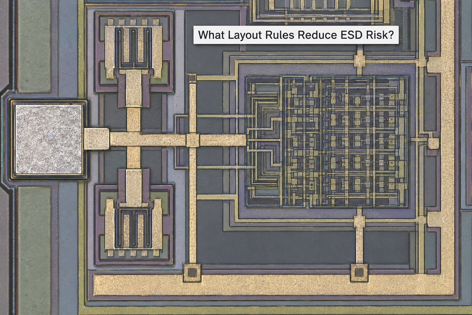
A correct schematic can still produce a dead part if the current path is wrong. These ten rules are the ones that most often decide whether a protection network works.
- Put the clamp directly under the pad. Distance is response time. A clamp a few hundred microns away cannot catch a sub-nanosecond CDM edge.
- Keep the clamp loop short and wide. Loop inductance scales with area. A tight rectangle beats a long thin trace at every current level.
- Tie the return to a rail that is actually connected. A clamp feeding a floating rail protects nothing. A rail that floats under an ESD event is a common and expensive error.
- Use adjacent rail taps, not a shared distant rail. Give each I/O cell a local connection to the pad ring rail so the current does not travel along the ring through other cells’ pins.
- Add guard rings around injection points and deep trench isolation where the process offers it. The guard ring collects carriers and keeps them out of the core.
- Keep the return path independent of the signal path. Do not let discharge current return through the pad’s own signal trace or through a shared bond pad that also carries functional current.
- Route symmetrically on differential and high-speed pairs. Asymmetric clamp connections add an unbalance that shows up as signal integrity degradation even when the part passes ESD.
- Separate the clamp from sensitive analog nodes. Substrate coupling travels further than you expect. Keep the analog guard structures between the sensing pad and the high-current clamp.
- Size the metal for peak current, not average current. A discharge is short and violent. Thin metal that passes DC current can melt during a pulse.
- Follow the ESD-CMOS layout rules your foundry publishes. The foundry knows its own parasitic structures and its own latch-up triggers. Their rules are not generic.
One more practical habit pays off. Review the layout the way you would review a signal integrity problem, with current flow in mind rather than net connectivity. Ask where the electrons go, and how long they take to get there.
How Can Engineers Verify ESD Protection?
Verification runs from the schematic through to the packaged part, and each stage catches a different class of mistake.
Step 1: schematic and specification review. Confirm every externally reachable pin has a defined stress model, a clamp device, and a return rail. Record the working voltage, the clamp voltage, and the leakage budget for each node. This is where you find the pin nobody protected.
Step 2: parasitic extraction and simulation. Extract the real interconnect and device parasitics from the layout, then simulate the clamp’s dynamic resistance and the pad’s voltage response using a transmission line pulse, or TLP, waveform. TLP is the industry tool of choice because it matches the rise time and duration of a real discharge far better than a static curve.
Step 3: device-level qualification. Run HBM and MM per JEDEC JS-001, and CDM per JS-002, on the packaged parts. Common qual levels for HBM are 2 kV, 4 kV and 8 kV for human exposure, with 15 kV and 25 kV used in some machine-readable and automotive contexts. Automotive parts carry an additional AEC-Q100 expectation on top of the JEDEC baseline.
Step 4: system-level testing. A chip that passes every device-level test can still fail on the board. IEC 61000-4-2 contact and air discharge on the assembled product is the check that closes the loop, and it is where board-level TVS placement gets judged.
Pass criteria you should record for each protected pin: peak clamp voltage stays below the victim’s absolute maximum rating including margin, leakage at the maximum operating temperature stays inside the circuit’s budget, leakage recovers to nominal after stress, functional behavior is unchanged before and after, and there is no parametric shift that grows over repeated strikes.
That last one catches latent damage, which is the failure mode factory testing is worst at finding.
What Common ESD Design Mistakes Should Be Avoided?
These show up over and over, and each has a straightforward fix.
Oversized clamps. A clamp with more current capacity than the pad can ever see wastes die area and adds capacitance you do not need. Size to the stress model, not to the largest number in the datasheet.
Excessive capacitance on a fast node. The clamp degrades edge rate and can cause eye closure on a link that passed simulation with an ideal pin. Match total pin capacitance to the interface budget, and put a low-capacitance diode in parallel if the budget is tight.
Wrong working voltage. A clamp that conducts at a voltage the signal legitimately reaches is worse than no clamp, because it corrupts data. Check the maximum operating voltage at the hot corner, not the typical value.
Poor return paths. A correct clamp with a long, inductive return produces a voltage overshoot at the pad that is higher than the clamp’s own breakdown voltage. This is the single most common reason a well-designed network fails CDM.
Floating rails. A clamp tied to a rail that is not solidly connected anywhere nearby gives the pulse nowhere to go. Taps and rail straps in the pad ring fix it.
Unprotected pins. Pins get left off by accident when a pad is added late, or deliberately when a designer assumes the system will protect it. Record the decision either way.
Excessive series resistance. A large series resistor slows the pulse and spreads the energy, which is useful on a slow signal and destructive to a fast one. Use it deliberately and only where the interface budget allows.
Routing surge current through sensitive circuitry. If the discharge current returns through the analog section or through a shared functional pad, the ESD event becomes a functional glitch that may not fail the test but will show up in the field.
On-chip protection also does not remove the need for handling discipline. Wrist straps, grounded benches, ionized airflow and ESD-safe packaging in the fab and assembly flow are all still part of the answer. ESD accounts for a large share of field failures, and no die-level network is a substitute for not generating the event in the first place.
Frequently Asked Questions
What is the difference between ESD protection and surge protection?
Surge protection handles slower, higher-energy events such as lightning and switching transients, while ESD protection handles very fast, low-energy discharges lasting nanoseconds. They use different standards, different device physics and different clamps. A design that passes an IEC 61000-4-2 system surge test can still fail an HBM or CDM device test, which is why chips need both.
Should every chip pin have an ESD protection circuit?
No, and pretending otherwise costs die area you may need elsewhere. External signal pins normally get protection, along with rails and exposed package connections. Power switching nodes on power ICs usually do not, because a clamp across a switching node would conduct during normal operation. Internal-only nets need nothing because no discharge can reach them. Document the decision per pin rather than relying on convention.
How low must the capacitance of an ESD protection device be?
Low enough that the interface budget still closes. On a slow GPIO, a few hundred femtofarads is usually fine. On a multi-gigabit link, total pin capacitance has to sit under roughly 0.5 pF including the package. Compute the budget from the rise time you need, then subtract package and pad capacitance before selecting a clamp. ESD protection in chip design is where that budget gets spent, so decide the interface first.
Why does ESD protection need a short ground return path?
Because the return path is an inductor, and the voltage across a pad is the clamp’s threshold plus the IR and L di/dt drop of the current returning. A long, narrow return turns a 6 V clamp into a 30 V pad excursion. Keep the loop short, wide and physically adjacent, and tie it to a rail that is solidly connected nearby. This single layout decision causes more CDM failures than device choice does.
What should engineers do when a chip fails an HBM or CDM test?
Start by classifying the damage: parametric shift, functional failure, or complete failure. Then check the usual suspects in order, starting with return path inductance and floating rails, then clamp sizing and working voltage, then unprotected pins or substrate coupling. Re-extract parasitics from the actual layout and simulate with a TLP waveform. A CDM failure with an HBM pass almost always points to layout, not to the clamp device itself.
Conclusion
Start with a list, not a device. Identify every external connection on the die, assign each one its stress model and its functional constraints, and write down which pads are being protected and which are being left alone on purpose.
Then select a clamp that fits inside the ESD design window for that node, and design the return path before you worry about anything else. Short, wide, adjacent, tied to a rail that is actually connected.
Only after the layout is extracted and simulated should the part go to qualification, because a network that has not survived TLP simulation is not going to surprise you well at HBM or CDM test. The physics has been settled for decades; the failures still come from skipping the list.