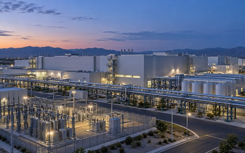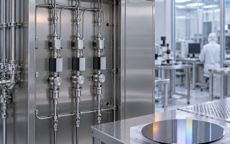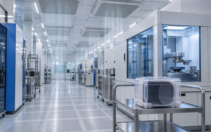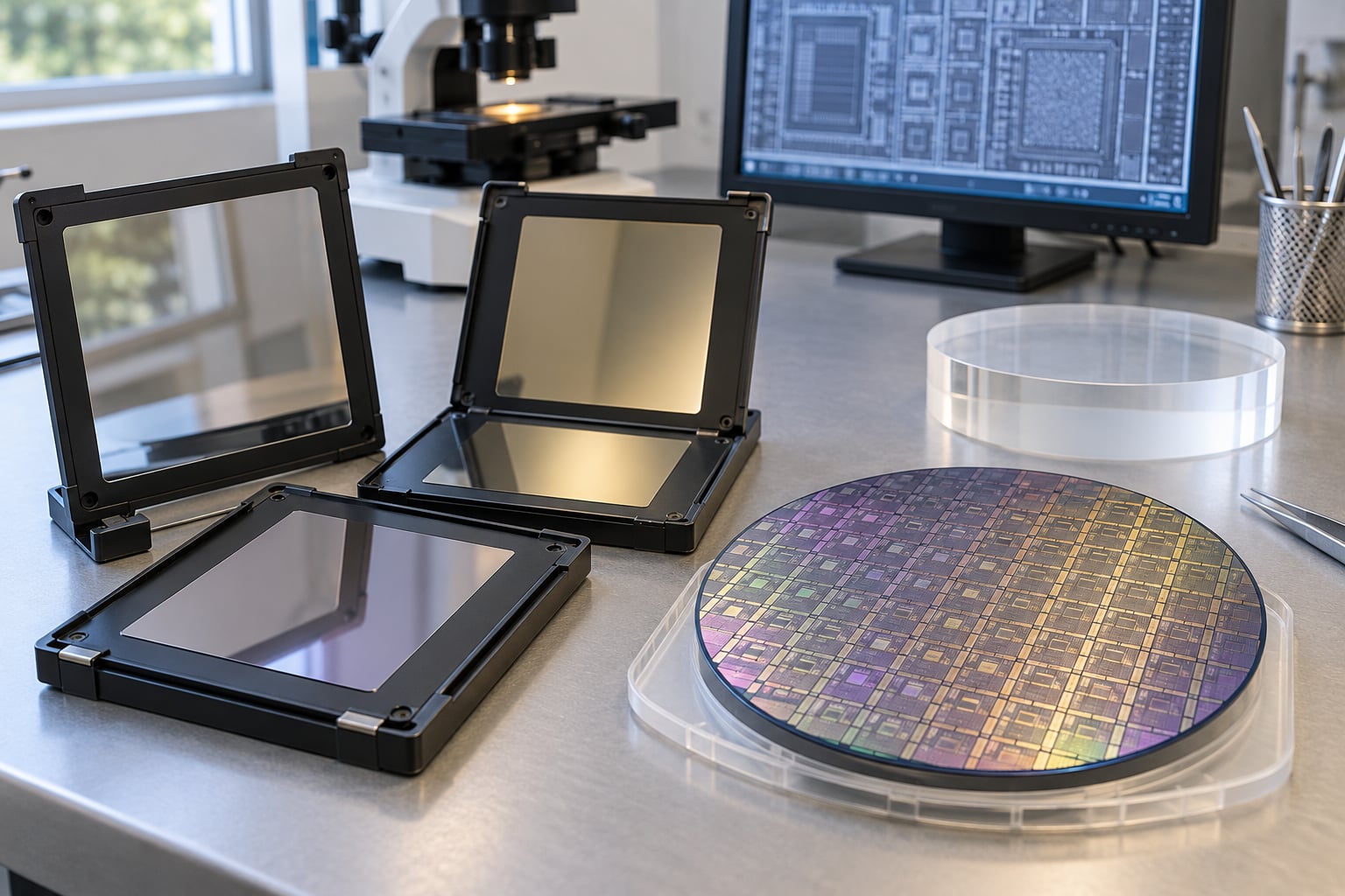
A mask set is the complete, matched group of photomasks a single chip design needs, one for every lithography layer, written and shipped together as one deliverable. What a mask set is and why it costs so much comes down to four steps that get harder at every node: electron-beam writing, computational shape correction, inspection, and repair at ever tighter tolerances. Those steps push a single mask from tens of thousands of dollars at mature nodes to three to five million dollars at the leading edge, and a full 3nm set into the thirty-to-fifty-million-dollar range that engineers argue about on every tape-out.
If you have a tape-out quote and no idea which number applies to you, this guide sorts the figures out and shows where the money actually goes. All costs below are typical US ranges. They vary by region, by supplier, and over time, so treat them as order-of-magnitude anchors rather than quotes.
Table of Contents
- What a Mask Set Is and What It Costs
- What one photomask is made of
- Mask, reticle, pellicle, mask set: the terms people mix up
- How many masks are in a mask set
- What a mask set costs, from mature nodes to 2nm
- What Affects the Price
- Where the money goes in one advanced mask
- Why multiple patterning multiplies the bill
- EUV trades fewer masks for more expensive ones
- Inspection, defect repair and mask turnaround time
- Who actually makes the masks
- Why published 3nm figures disagree
- Ways to Save
- Work out the amortization before you commit
- Cut layers and multi-patterning where the design allows it
- Reuse a verified mask and freeze the design
- Decide the mask strategy before you spend the compute
- Sometimes you should not buy a mask set at all
- Frequently Asked Questions
- What is a semiconductor mask set?
- How many photomasks does a chip need?
- Why do smaller process nodes cost more for mask sets?
- Are EUV mask sets more expensive than DUV mask sets?
- Can engineers reuse photomasks for multiple chips?
- How much does a low-volume prototype mask set cost?
- The Bottom Line
What a Mask Set Is and What It Costs
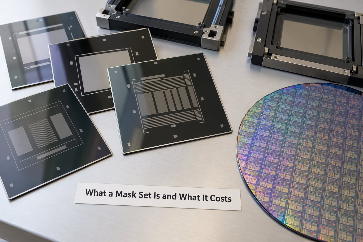
A mask set is every photomask one design needs, and it is priced as the sum of dozens of individually written, inspected and qualified reticles rather than as a single object. The set is built once, at tape-out, then reused for every wafer that fab runs from that design.
What one photomask is made of
A photomask is a square plate of fused silica roughly the size of a dinner plate, coated with a metal absorber film. Transparent areas of the film pass light, opaque areas block it, and that pattern is what prints onto the wafer’s photoresist.
Modern masks are not simple clear-and-opaque plates. They carry sub-resolution assist features, small assist shapes that make a dense pattern print cleanly at a wavelength far too long to resolve it directly. They can also use phase shifting, where a transparent layer delays the light slightly so two neighbouring patterns interfere constructively instead of cancelling.
Each plate sits in a holder with a pellicle, an ultrathin transparent membrane a few micrometres above the pattern that traps particles before they land on the mask. The pellicle is cheap insurance and it is also a headache, because a speck on a pellicle prints onto every wafer that uses the reticle.
Mask, reticle, pellicle, mask set: the terms people mix up
Mask, reticle and mask set are used interchangeably in conversation but not in a mask shop. Here is the split that keeps a purchase order unambiguous.
| Term | What it actually is | Where it lives in the flow |
|---|---|---|
| Mask | The physical plate carrying the pattern, blank plus absorber film | In the supplier’s cleanroom until it is mounted |
| Reticle | A finished, inspected, pellicle-covered mask in its holder, qualified for a specific scanner | Loaded into the lithography scanner at the fab |
| Pellicle | Transparent protective membrane mounted a few micrometres above the pattern | Part of the reticle assembly |
| Mask layer | One exposure step in the process, such as metal one or the active layer | One photo pass per wafer |
| Mask set | All mask layers for one design, matched and qualified together | The NRE deliverable a designer buys at tape-out |
How many masks are in a mask set
A mask set typically contains 30 to 80 masks, and the count has been climbing rather than shrinking. An eBeam Initiative survey cited by Semiconductor Engineering put the number at 60 masks per set at 16nm and expected 77 below 11nm. Most of that growth comes from multi-patterning, where one dense layer is split into two or three exposures.
A mature 180nm part might need 12 to 15 masks. A leading-edge logic design needs three times that. A memory design can run higher still, since stacked devices reward aggressive layer-to-layer patterning.
What a mask set costs, from mature nodes to 2nm
Cost per mask climbs by roughly two orders of magnitude between 180nm and 3nm, and cost per set climbs faster because mask count is climbing at the same time. The 2006 anchor most people still quote, one thousand to one hundred thousand dollars for a single high-end phase-shift mask with up to 30 masks in a complete set, describes a world that no longer exists.
| Technology node | Typical masks per set | Typical cost per mask | Typical cost per mask set |
|---|---|---|---|
| 180nm | 12 to 15 | 1,000 to 5,000 dollars | 15,000 to 50,000 dollars |
| 130nm | 15 to 18 | 3,000 to 10,000 dollars | 50,000 to 150,000 dollars |
| 90nm | 18 to 22 | 8,000 to 20,000 dollars | 150,000 to 400,000 dollars |
| 65nm | 20 to 25 | 20,000 to 40,000 dollars | 500,000 to 900,000 dollars |
| 40nm | 25 to 30 | 40,000 to 70,000 dollars | 1 to 2 million dollars |
| 28nm | 30 to 40 | 60,000 to 100,000 dollars | 2 to 4 million dollars |
| 16nm | 45 to 60 | 100,000 to 200,000 dollars | 5 to 10 million dollars |
| 7nm | 50 to 65 | 150,000 to 300,000 dollars | 10 to 20 million dollars |
| 5nm | 55 to 70 | 250,000 to 500,000 dollars | 20 to 30 million dollars |
| 3nm | 60 to 80 | 500,000 to 1,000,000 dollars for DUV; 3 to 5 million dollars for EUV masks | 30 to 50 million dollars |
| 2nm | 60 to 80 | 3 to 5 million dollars for EUV masks | Reported above 40 million dollars |
The high-NA EUV systems now moving into production complicate that picture further. A single EUV blank with a reflective multilayer absorber runs several hundred thousand dollars before a single beam is written, and defect inspection at that wavelength is demanding enough that the per-mask line item keeps moving.
What Affects the Price
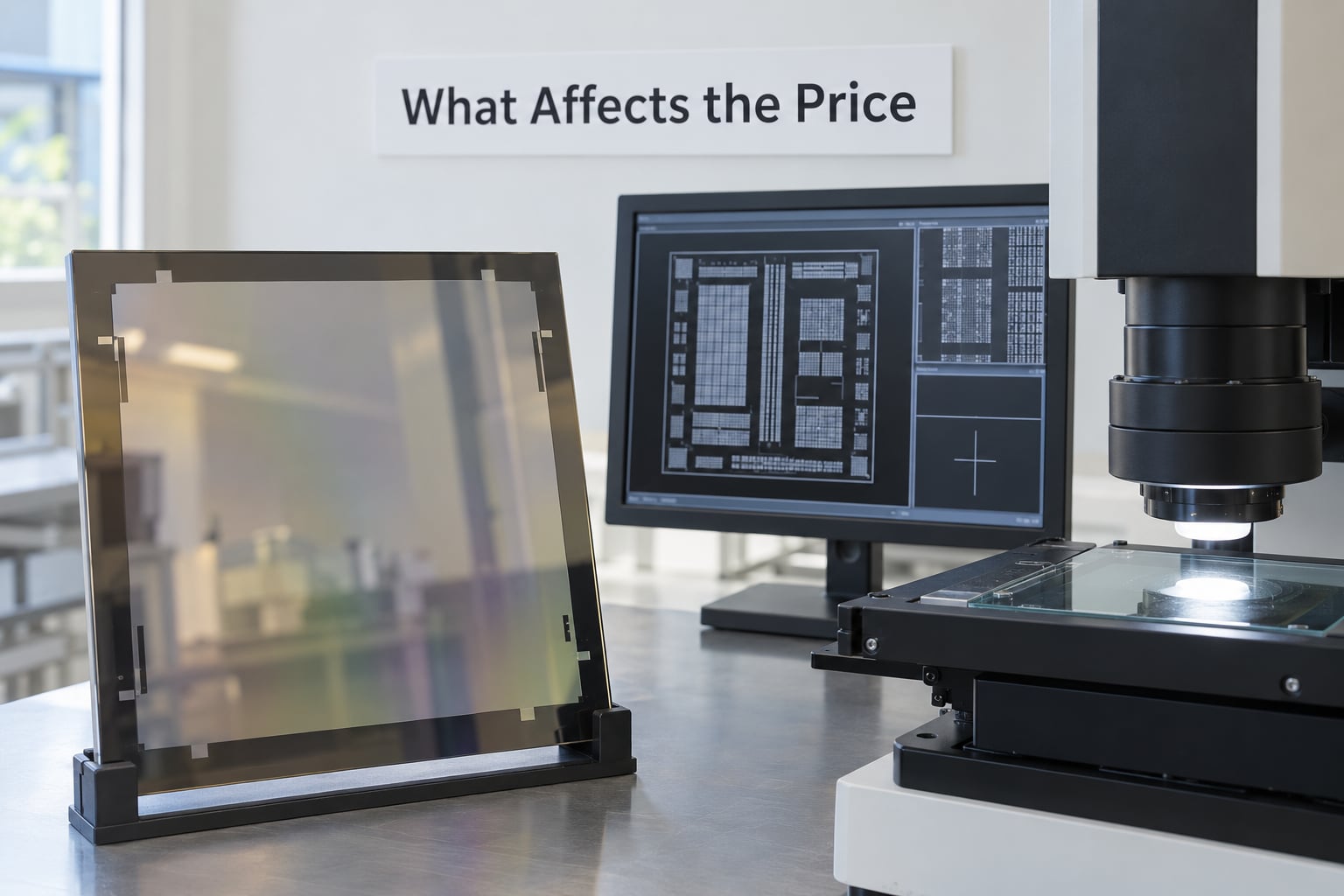
Mask price tracks two variables above all else: how long the writer has to deposit electrons, and how tightly the pattern has to land. Both get worse with every node, and everything else in the price follows from them.
- Write time. An electron-beam writer paints the pattern one small spot at a time. As half-pitch shrinks, the spot count grows faster than the wafer area shrinks, so exposure time per mask climbs steeply. A multi-beam writer parallelises this work, but each added beam adds to the capital cost of the tool that every mask price has to cover.
- Computational correction. Optical proximity correction and inverse lithography technology reshape the mask so the printed pattern lands where the design intended. Model-based processing with GPU acceleration has largely replaced classical mask fracturing at advanced nodes, and that compute time sits inside the mask order.
- Blank materials. A fused silica blank is cheap by fab standards. A multilayer EUV blank with a reflective coating stack and a defect-free absorber is not, and the price gap between a DUV blank and an EUV blank is the single hardest number in any mask quote.
- Inspection and repair. Advanced-node masks are inspected at near-atomic resolution and repaired with a nanometer-scale beam. Every inspection pass and every repair cycle adds hours, and each one can send the mask back for another pass.
- Set logistics and storage. A mask set is not 60 loose plates. It is a qualified, matched, cleaned and packaged set with tracking, storage and requalification for a specific scanner, and a design that changes late can force requalification of the whole set.
Where the money goes in one advanced mask
Writing and inspection account for the majority of the cost on an advanced mask, while the blank is a minority of the total despite being the part everyone pictures. Shares shift by node and by supplier, so read this as a shape, not an invoice.
| Cost element | Share of a leading-edge mask | Why it scales |
|---|---|---|
| Mask write time | 30 to 45 percent | Spot count rises faster than area shrinks |
| Inspection and metrology | 15 to 25 percent | Tighter resolution and more defect classes to catch |
| Mask blank | 10 to 20 percent | EUV blanks cost multiples of DUV blanks |
| OPC and ILT compute | 5 to 15 percent | Model-based processing runs on GPUs per mask |
| Repair cycles | 5 to 10 percent | More passes as defect sensitivity tightens |
| Handling, packaging, storage | 3 to 8 percent | Cleanroom-grade logistics for a qualified set |
Why multiple patterning multiplies the bill
Multiple patterning is the clearest case of mask cost running on geometry alone. When a dense layer cannot be printed at a given pitch, it gets split across two exposures: one mask for the vertical spacings, one for the horizontal, and both must land on the same wafer. Self-aligned double patterning and quadruple patterning push this further.
Each split adds a layer to the mask set, an extra photo pass on every wafer, and extra process steps. A design that used single patterning at 15 masks per set can carry 60 or more at the same nominal node once double patterning is applied. This is why mask count per node rose even as feature sizes fell.
EUV trades fewer masks for more expensive ones
EUV at 13.5nm prints a layer with one exposure where 193nm immersion needs two or three, so a 3nm design should carry fewer mask layers than a comparable 7nm design built on immersion. Practitioners describe this on LinkedIn as EUV reducing mask layers and, in practice, the layer count does come down.
The trade is that each EUV mask costs far more to make than a DUV mask. Fewer masks at higher unit price still leaves the set more expensive, which is why a practitioner post on 3nm scaling still names the mask set as the biggest single cost driver.
Inspection, defect repair and mask turnaround time
A mask defect that would have been harmless at 90nm can print a shorted transistor at 3nm. Inspectors use actinic inspection at the exposure wavelength, so a defect smaller than a wavelength still gets caught, and repair uses a focused beam to patch a single absorber feature in place.
Turnaround time is the schedule cost nobody prices explicitly. Write, inspect, repair and re-inspect can run weeks per mask, and the masks are worked in parallel, so a 60-mask set is a months-long programme with a real chance one mask comes back from repair needing a second pass.
Who actually makes the masks
Most masks are made by merchant suppliers rather than in-house, though the largest IDMs still run captive mask shops. Merchant names you will see on a purchase order include Tekscend Photomask, Toppan Photomask, DNP and Photronics, with DNP and Toppan carrying much of the 3nm and 2nm EUV work. An industry-cited share figure puts Tekscend near 39 percent of the merchant market.
Foundries typically route mask orders through a qualified supplier list tied to the node, so the designer rarely chooses the shop directly. What the designer does control is the number of layers, the mask strategy, and how early the design is frozen.
Why published 3nm figures disagree
The disagreement you will find in forums and LinkedIn posts is mostly a units problem, not a scandal. One camp quotes thirty to fifty million dollars for a full 3nm set. A Hacker News thread cites above forty million dollars. Market-research pages quote three to five million dollars, but that is a per-mask figure at 3nm and 2nm, not a set.
Another camp still quotes one thousand to one hundred thousand dollars per mask. That is a 2006 figure for a high-end phase-shift mask, and treating it as current is the most common error in internal cost models.
Ways to Save
The biggest saving is not negotiating with a mask shop. It is not needing as many masks, and not needing them twice. Mask cost is a one-time NRE amortized across every wafer in the run, so the question is always volume per mask set.
Work out the amortization before you commit
Take a forty-million-dollar mask set. Spread it across 10,000 wafers and you carry four thousand dollars per wafer before a single defect is counted. Spread it across one million wafers and it falls to forty dollars, which disappears into the process cost. The same set, the same price, two completely different decisions.
This is the arithmetic practitioners reach for immediately. In the Hacker News discussion of 3nm mask cost, the first response was not about writing tools at all but about how many chips a set like that would need to move before it stopped mattering.
Cut layers and multi-patterning where the design allows it
Every mask removed from the set is removed from the write queue, the inspection queue and the wafer cycle. Design-for-manufacturability reviews that trade a little die area for a shared mask layer are often worth more than they look, because a shared layer costs one mask instead of two overlapping exposures.
Cell padding, standard cell alignment and staying inside the foundry’s preferred patterns all reduce the corrective features the writer has to place, and corrective features are what drive write time up.
Reuse a verified mask and freeze the design
Masks are reusable across wafers by design, and across designs when the layers are identical. A related product that shares seven or eight masks with one already qualified can cut the new set down to a handful of layers plus requalification. Requalification is not free, but it is cheaper than rewriting the shared layers.
Late changes are the expensive part. A change that lands after a mask is written usually costs a new mask for that layer and a wait for the whole set to be re-matched.
Decide the mask strategy before you spend the compute
Whether a layer will be single-patterned, self-aligned double-patterned, or EUV-only changes the mask count and the schedule, and it is far cheaper to decide at architecture stage than after the OPC results are in. The same applies to the memory compiler choices that drive the densest layers.
Sometimes you should not buy a mask set at all
For prototype ASICs, low-volume sensors and any design that will never reach volume production, a mask set is often the wrong purchase. Three alternatives exist, and each trades a different cost for a different constraint.
| Approach | Mask cost | What it costs instead | Best for |
|---|---|---|---|
| Full custom mask set | Thousands to tens of millions of dollars | Months of mask write time and tape-out NRE | Volume production |
| Multi-project wafer shuttle | Share of a shuttle mask set | Fixed die area, shared process, no volume path | Design verification, proof of concept |
| E-beam direct write | No mask set | Very slow per wafer and expensive per wafer hour | Prototype and low-volume runs |
| Maskless lithography | No mask set | Throughput and feature size limits | Niche and research work |
Market-research figures put a prototype ASIC mask set at one to five million dollars, which is exactly the line e-beam direct write is often used to avoid. The trade is real: direct write removes mask NRE and buys you slow wafers.
Frequently Asked Questions
What is a semiconductor mask set?
A mask set is the complete group of photomasks one chip design needs, with one mask for every lithography layer in the process. Each mask is written by an electron-beam writer, inspected, repaired and mounted with a pellicle, then all of them are qualified together against a specific scanner. A mask set is bought once at tape-out as NRE and reused for every wafer produced from that design.
How many photomasks does a chip need?
It depends on the node and the patterning strategy. A mature 180nm design needs roughly 12 to 15 masks, while an eBeam Initiative survey cited by Semiconductor Engineering counted 60 masks per set at 16nm and expected 77 below 11nm. Leading-edge sets now land somewhere between 60 and 80 masks, and multi-patterning is the main reason the count keeps rising.
Why do smaller process nodes cost more for mask sets?
Three things happen at once. Features get finer, so write time per mask rises because the writer deposits far more spots. Patterns need heavier OPC and ILT correction, which adds compute and adds shapes to write. And dense layers need multiple patterning, which adds whole extra masks to the set. Fewer, harder masks times more masks per set equals a much larger NRE bill.
Are EUV mask sets more expensive than DUV mask sets?
Per mask, yes by a wide margin, because EUV blanks carry a reflective multilayer absorber that costs several times a DUV blank and actinic inspection is harder. Per set, EUV usually still costs more, but it is the trade people miss: EUV collapses what would be two or three immersion exposures into one layer. You buy fewer, far more expensive masks instead of many cheap ones.
Can engineers reuse photomasks for multiple chips?
Yes, and teams do it constantly. A mask is reusable across every wafer of the same design for free, since it is already paid for. Across different designs, layers that are identical can be reused, so a related chip may need only a handful of new masks plus requalification. What is not reusable is a layer whose pattern differs, which has to be rewritten at full cost.
How much does a low-volume prototype mask set cost?
Prototype and low-volume designs fall in the range of one to five million dollars for a full set, depending heavily on node and how many layers the process needs. That is why e-beam direct write is common for prototypes: it eliminates the mask set entirely at the cost of very slow, expensive wafers. If volume is uncertain, shuttles and direct write often beat buying masks.
The Bottom Line
A mask set is a one-time NRE item that gets reused on every wafer in the run, and its price tracks write time, correction compute, blank materials and inspection passes. First step: take the mask-set line from your tape-out quote, divide it by the wafers you actually plan to run, and see whether the per-wafer number changes the plan. If it does, the design is asking for e-beam direct write or a shuttle run instead.