Why fabs use ultrapure water is simple: the wafer surface is the product, and any particle, metal ion, silica colloid or organic film that lands on it becomes a defect. Modern nodes have features measured in nanometres, so a speck too small to see is large enough to etch or short a transistor. Ultrapure water, or UPW, is the cleaning medium that leaves the surface with nothing on it.
The practical standard is water with resistivity above 18.2 MΩ·cm at 25°C, total organic carbon under 1 part per billion, and particle counts held low at sizes the metrology can actually see. SEMI F63 and ASTM D5127 describe the specification; roadmap documents such as the ITRS and the current IRDS describe how tight it has to be for a given node.
A few things to hold on to before the detail:
- UPW does not just rinse dirt off. It is the base medium for wet etch, solvent processing, chemical mechanical planarization, chemistry blending and tool cooling.
- Every specification traces back to a specific defect mechanism, not to a general aspiration for cleanliness.
- Clean water going into a fab is only part of the story. Materials of construction, dead legs, flow velocity and biofilms decide whether the water stays clean on the way to the wafer.
- Fabs withdraw far more water than they consume, because most of it is reused after reclamation.
Table of Contents
- What Is Ultrapure Water and Why Do Fabs Use It?
- Why fabs use ultrapure water instead of ordinary laboratory water
- How Pure Water Protects Wafers and Equipment
- Metal ions and gate oxide reliability
- Colloidal silica and lens hazing
- Organics, particles and biofilm
- Killer particles shrink with every node
- Where Fabs Use Ultrapure Water
- Wafer cleaning and rinsing
- Wet etch and solvent processing
- CMP slurry preparation and post-CMP cleaning
- Chemistry blending and tool cooling
- How much water a wafer actually takes
- How Semiconductor Fabs Produce Ultrapure Water
- What Purity Specifications Mean for Chip Manufacturing
- How Contamination Control Affects Yield and Cost
- Frequently Asked Questions
- Is ultrapure water the same as distilled water?
- How does water contamination cause defects in semiconductor chips?
- Does ultrapure water eliminate all contamination during wafer processing?
- Why can semiconductor fabs not reuse water without additional treatment?
- What quality controls do fabs use to monitor ultrapure water?
- Is ultrapure water safe to drink in a semiconductor fab?
- What to Take Away First
What Is Ultrapure Water and Why Do Fabs Use It?
Ultrapure water is deionized water taken past the point where a normal DI system stops. Ion exchange or reverse osmosis removes most dissolved salts, then a series of polishing steps strips the residue those systems leave behind: trace ions, silica, organics, particles and bacteria.
The headline number most engineers quote is 18.2 MΩ·cm, which is close to the 18.25 MΩ·cm theoretical maximum for water at room temperature. Resistivity on its own is a blunt instrument, though. A well-run DI loop can read 15 MΩ·cm and still carry organics, colloids or a biofilm that no conductivity probe can see, which is why UPW specifications are always a bundle of numbers rather than one figure.
Why fabs use ultrapure water instead of ordinary laboratory water
Laboratory water is purified for general analytical work. UPW is purified against a defect budget. The difference shows up in what each specification is aimed at: a lab spec targets the accuracy of an experiment, while a UPW spec targets the probability of a wafer surviving a process step. That is why UPW limits tighten as node dimensions shrink, and why the same loop that met the spec at 28 nm needs an upgrade for 2 nm.
| Parameter | Typical fab target | Why it matters |
|---|---|---|
| Resistivity | Above 18.2 MΩ·cm at 25°C | Bulk proxy for remaining dissolved ions |
| Total organic carbon | Below 1 ppb, tightened further for immersion lithography | Organics form films and haze optics |
| Particles | A few per mL at 0.05 µm and below | Killer particles print onto the wafer |
| Dissolved silica | Low single-digit ppb | Colloidal silica deposits as haze |
| Dissolved oxygen | Low single-digit ppb | Avoids oxidation at sensitive surfaces |
| Bacteria | Below detection on a live count | Biofilm sheds particles |
| Metals such as Na, Cu, Fe | Sub-ppb to ppt | Mobile ions poison gate oxides and contacts |
How Pure Water Protects Wafers and Equipment
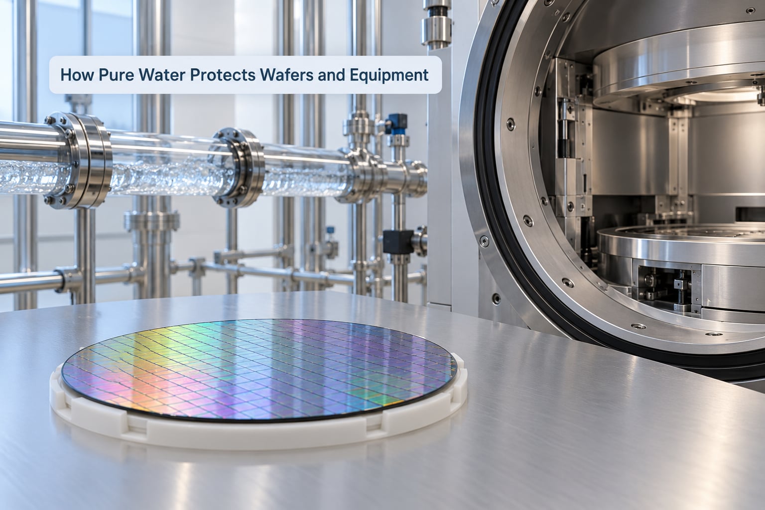
Each contaminant class has its own failure signature, and the failure usually shows up far from its cause. That is why contamination control gets treated as a discipline rather than a purchase order.
Metal ions and gate oxide reliability
Sodium, potassium, copper and iron at the parts-per-trillion level can migrate into thin gate dielectrics. The result is a shift in threshold voltage or a change in oxide lifetime, and because the damage happens at the atomic scale, it is not visible in a defect inspection. It surfaces weeks later as a reliability failure in the field.
Colloidal silica and lens hazing
Silica that has not fully dissolved behaves differently from the dissolved fraction. Colloidal particles attach to optics, and in immersion lithography, where water sits directly between the lens and the wafer, a buildup on the lens surface reduces transmission and can force a mask or scanner intervention. This is the single strongest argument for the tightest organic and particle limits in the fab.
Organics, particles and biofilm
Organic carbon above the spec leaves a film that blocks an etch or distorts a surface. Particles above the size limit become what process engineers call killer particles, because a single one landing on a critical area kills the die. Biofilm is the sleeper problem: it colonises pipe walls, valves and dead legs, and a mature film sheds particles continuously even while the water reads clean at the plant outlet.
Killer particles shrink with every node
This is the part that explains why the specs never stop tightening. As minimum feature sizes fall, so does the size of a defect that ruins a device. A 1 µm particle was harmless in a mature logic node and is a full chip killer in an advanced one. Roadmaps therefore push control toward sub-10 nm particles, and some ionic contamination targets now sit below the detection limits of the analytical tools available to measure them.
Equipment is affected too. Water is a process fluid and a heat-transfer fluid at the same time, and it runs hotter at each node. Dissolved solids scale inside nozzles and heat exchangers, and a scaling particle in the wrong place shortens pump and chamber life.
Where Fabs Use Ultrapure Water
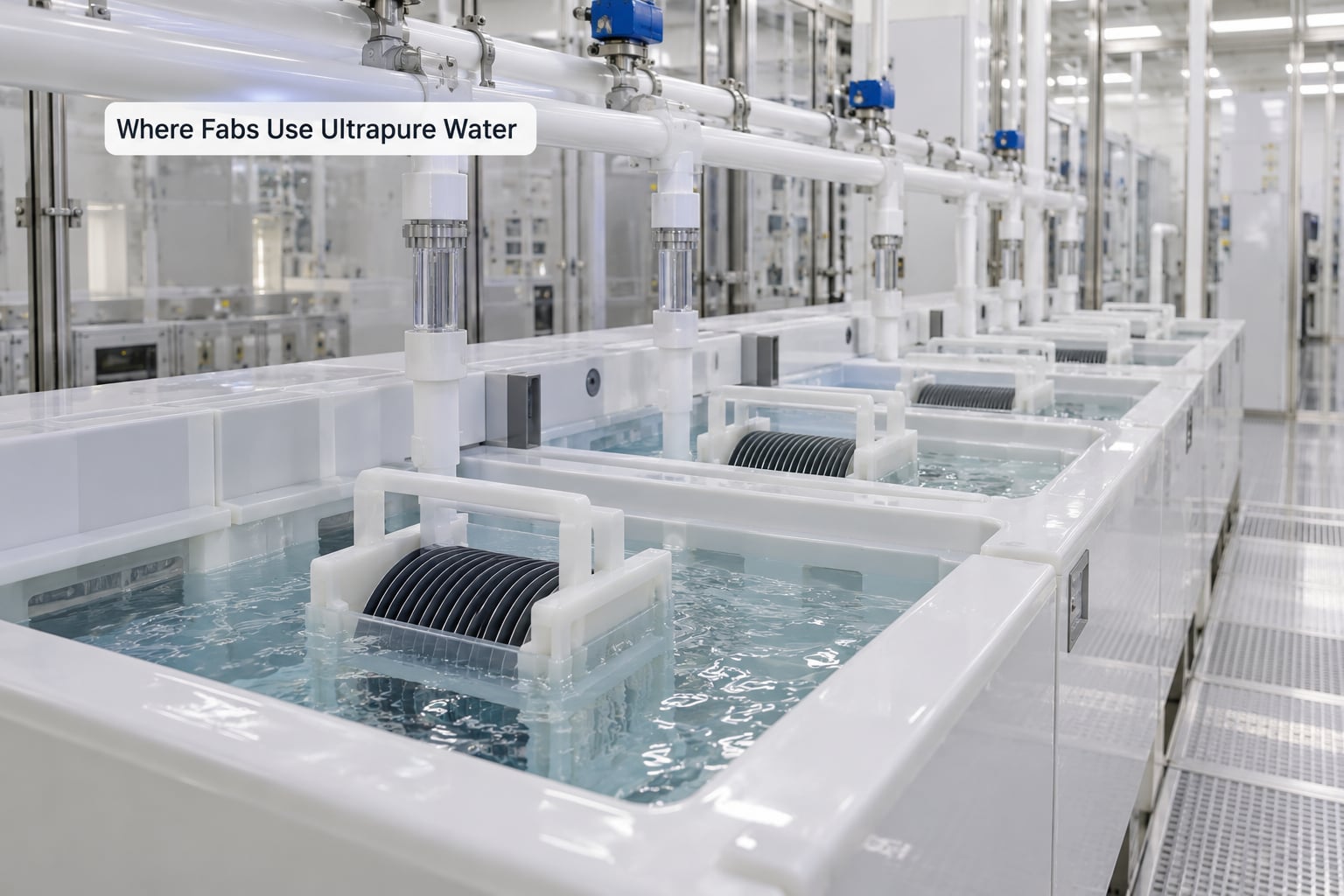
Ultrapure water touches the process in four broad ways, and understanding them separately is the fastest way to see why a fab runs a plant of this size.
Wafer cleaning and rinsing
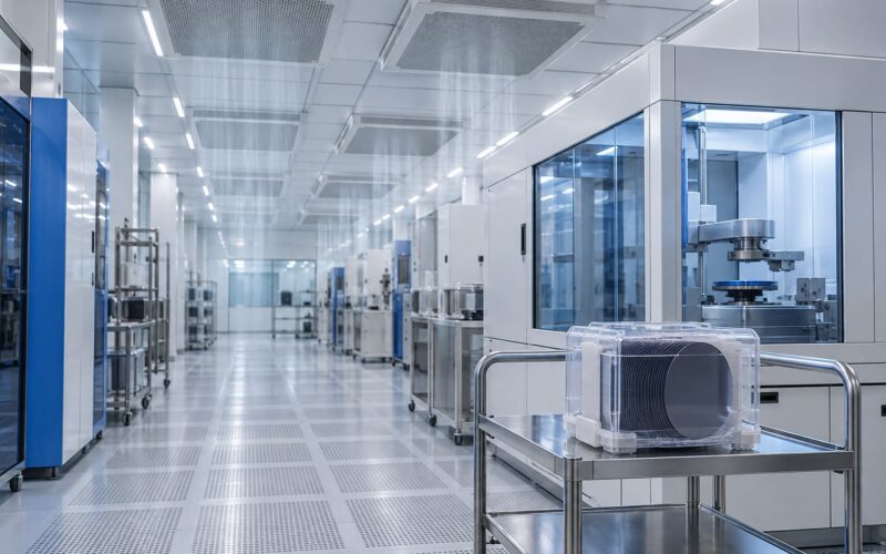
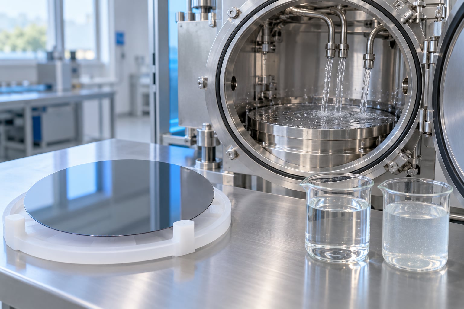
Particle cleaning, megasonic cleaning, and the numerous dilute hydrochloric, hydrogen peroxide and ammonia rinses that run between process steps all end in a final UPW rinse. This is the highest-volume use and the one with the tightest particle requirement, since the rinse is what leaves the surface in its pre-process state.
Wet etch and solvent processing
Wet etch baths are thinned and topped up with UPW to hold concentration steady across a batch. Solvent processes use it for the same reason on the other side of the tank: precision on concentration, and a rinse that leaves no residue behind. Both depend on the water being an inert, predictable component of a chemical recipe.
CMP slurry preparation and post-CMP cleaning
Chemical mechanical planarization slurry is mixed, diluted and delivered with UPW, then the wafer is cleaned again afterwards with a slurry-specific brush or pad clean and a final rinse. Slurry chemistry is sensitive to dilution water quality in a way that surprises newcomers, because the contaminants are often parts per billion but act on the chemistry as a whole.
Chemistry blending and tool cooling
Photoresist, etchant and developer blending lines use UPW as the primary diluent, which means a quality excursion shows up as a concentration drift rather than as a visible contamination event. Separately, UPW cools lithography scanners and wet-processing tools, and it carries spent chemistry to the drain system. Equipment makers such as MKS describe this cooling duty explicitly, since water that is clean for a wafer can still be unsuitable as a coolant if its temperature or ionic profile is wrong.
How much water a wafer actually takes
Published figures conflict because they measure different things. The ITRS reported about 7 litres per square centimetre of wafer at a wafer-out stage, with a target of 4.5 L/cm². A 200 mm wafer has roughly 314 cm² of usable surface on one side, which puts a single wafer in the neighbourhood of 1,400 litres at the target figure and around 2,200 litres at the 2011 measured figure. Multiply that across a production flow and you arrive at the thousands of cubic metres per day figures that appear in trade coverage.
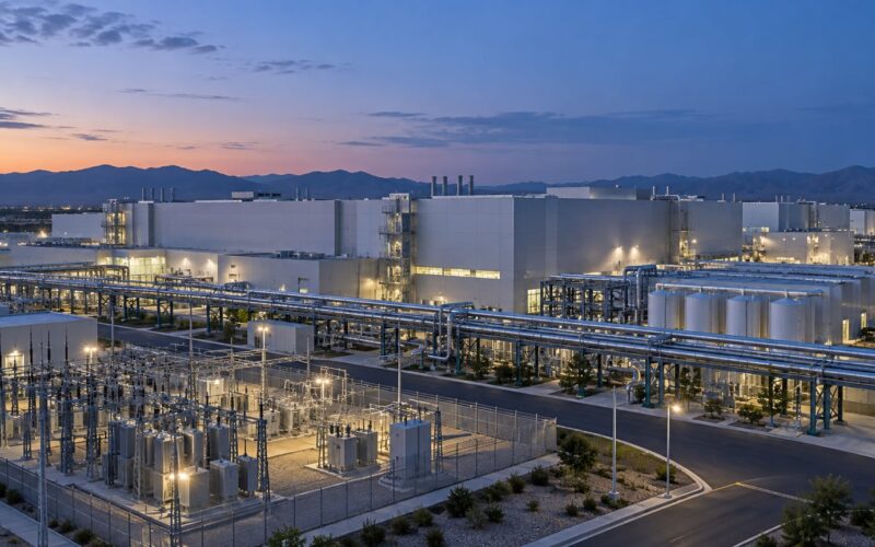
Withdrawal, reuse and consumption are three different numbers. A large fab may withdraw millions of US gallons a day from the municipal supply, produce several thousand cubic metres of UPW, and consume far less of either, because cooling towers and evaporation are the genuinely consumptive sinks. Vendor-published figures of 2 to 4 million gallons per day sit comfortably alongside the 3,000 m³/day figures once you account for the different basis of each number.
How Semiconductor Fabs Produce Ultrapure Water
The treatment train exists because each stage removes a class of contaminant the previous one cannot. This is the sequence a fab runs, and it is a numbered list for a reason: the order is fixed by chemistry.
- Media filtration and activated carbon. Sand, multimedia and carbon filters take out suspended solids, organics and chlorine that would damage membranes downstream.
- Softening and degassing.Ion exchange softening removes hardness, and membrane or vacuum degassing strips dissolved gases such as carbon dioxide and oxygen that would otherwise raise resistivity limits.
- Reverse osmosis. Roughly 95 to 99 percent of dissolved ions leave the water here, which does most of the load reduction cheaply.
- Electrodeionization or polishing DI. Continuous ion exchange under an electric field takes the conductivity down toward the megaohm range without the chemical regeneration burden of a full resin plant.
- Ultrafiltration. Membranes in the 10,000 molecular weight range remove colloids, silica particles, bio-organisms and the bulk of remaining particles.
- UV oxidation. A 185 nm lamp breaks down resistant organics into carbon dioxide and water. One by-product catches engineers out: the lamps can generate low levels of hydrogen peroxide, which needs managing downstream.
- Final polishing. Non-regenerable resin beds and a final ultrafilter at the point of use deliver the last increment of particle and ionic control, right where the water enters the tool.
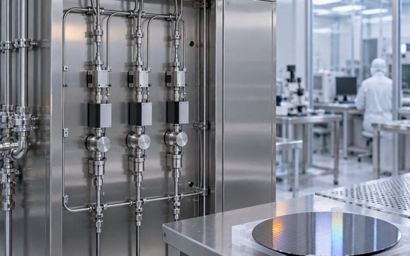
Once the water is clean, keeping it that way is a materials problem. Fabs specify high-purity fluoropolymers and electropolished stainless steel in contact loops, because sealants, gaskets and liners are a source of extractables that the water will pick up on the way to the wafer. Dead legs in the piping are a special case worth watching, since stagnant volumes harbour biofilm and shed particles into an otherwise clean loop.
What Purity Specifications Mean for Chip Manufacturing
Reading a UPW specification means knowing what each parameter can and cannot tell you. Resistivity is a bulk measurement and says nothing about particles or organics. Particle counts say nothing about dissolved metals. Only taken together do the numbers describe the water, and even then some limits sit below what current tools can see.
| Water type | Resistivity | Organic carbon | Typical use |
|---|---|---|---|
| Municipal tap water | 0.05 to 0.5 MΩ·cm | High | Plant feed, cooling |
| RO permeate | 0.2 to 1 MΩ·cm | Low | Feed to DI systems |
| Distilled water | 0.5 to 1 MΩ·cm | Moderate | General laboratory work |
| DI water | 1 to 15 MΩ·cm | Variable | General electronics and labs |
| Ultrapure water | Above 18.2 MΩ·cm | Below 1 ppb | Wafer processing |
Measurement follows the parameter. Resistivity comes from a conductivity probe, dissolved ions from ion chromatography, metals from ICP-MS, organic carbon from LC-OCD or online TOC analysers, silica from dissolved and colloidal measurements, and particles from laser light scattering or SEM capture filters at sub-0.2 µm sizes. Bacterial counts come from epifluorescence or standard culture methods, though live counts are far more informative than plate counts when biofilm is the question.
Fabs monitor the loop continuously and against statistical process control limits rather than a single pass or fail reading. An excursion is usually caught as a drift, which is why the plant keeps online analysers at multiple points of use rather than testing once a shift.
How Contamination Control Affects Yield and Cost
Yield is the number that makes a fab profitable, and defect density is the number that moves it. A water excursion that adds even a small number of particles per wafer compounds across every wafer in the affected lot, and those lots get held, reworked or scrapped. The direct cost is obvious; the larger cost is the schedule hit while the cause is being found.
Tool availability suffers in parallel. Contaminated water touches every wet tool on the line at once, so a single root cause can idle an entire wet-processing area. Because contamination is invisible in most cases, diagnosis is slow, which makes prevention more economical than rework in practice.
Reuse is where contamination control and economics meet. Fabs segregate drains by chemistry, and each category is reclaimed to a fit-for-purpose quality rather than pushed to full UPW. UMC reports about 84 percent process-water recycling across 27 separate drain categories, and ASE’s Kaohsiung facility sits around 70 percent. Vendor work on the input side puts municipal demand at roughly 1,400 to 1,600 gallons for every 1,000 gallons of UPW produced, and energy for treatment in the range of 3 to 7 kWh per 1,000 gallons.
The ceiling on all of it is purity. As node dimensions fall and sub-10 nm particle control becomes the requirement, the fraction of water that can be reused without extra treatment shrinks, because a reclaimed stream has to meet the tighter spec. Wastewater treatment adds its own pressure: PFAS monitoring has reached a 4 parts-per-trillion federal drinking water limit, and TMAH-bearing developer waste needs its own handling, which is why some sites are evaluating zero liquid discharge.
Frequently Asked Questions
Is ultrapure water the same as distilled water?
No. Distilled water condenses steam to remove most minerals and typically reaches 0.5 to 1 MΩ·cm, which is enough for general laboratory work. Ultrapure water exceeds 18.2 MΩ·cm, keeps organic carbon under 1 part per billion, and controls particles down to 0.05 µm and smaller. Both start as deionized water, but the polishing stages, filtration and monitoring behind UPW are what separate the two.
How does water contamination cause defects in semiconductor chips?
Particles land on the wafer and print onto layers that are later etched, leaving an open circuit or a short. Dissolved metals migrate into thin gate oxides and shift transistor behaviour. Colloidal silica attaches to optics, and in immersion lithography it can haze the lens and cut light transmission. Organics leave films that block an etch or leave residue after a rinse.
Does ultrapure water eliminate all contamination during wafer processing?
No. It removes an extremely low level of contaminants, but chemistry, wafer handling and tool materials can add more. Fab-grade water also cannot detect everything: some ionic contamination targets at advanced nodes now sit below the detection limits of available analytical tools. That is why control relies on materials of construction, flow velocity and clean-in-place discipline as much as on the water itself.
Why can semiconductor fabs not reuse water without additional treatment?
Because a spent process stream carries whatever the wafer carried. Depending on the step, that means metals, silica, dissolved organics, developer chemistries such as TMAH, and particles. Fabs therefore segregate drains by chemistry and reclaim each category to a fit-for-purpose quality rather than to full UPW. A reclaim stream that is fine for one step can ruin another if used without the right polishing.
What quality controls do fabs use to monitor ultrapure water?
Online analysers track resistivity, total organic carbon, dissolved oxygen and particle counts continuously, and plants watch those readings against statistical process control limits so a drift is caught early rather than a step change. Ions come from ion chromatography, metals from ICP-MS, silica from dissolved and colloidal measurements, and sub-0.2 µm particles from SEM capture filters or laser light scattering. Points of use are monitored separately from the plant outlet.
Is ultrapure water safe to drink in a semiconductor fab?
It is not dangerous to swallow, but it is not drinking water either. With almost no dissolved minerals and no bacteria, it will not hydrate you properly and it is not regulated as potable. Fab staff do not drink it, and it is routed to the drain system. Quora and forum threads ask this constantly because the answer is genuinely counterintuitive: the same water that is essential to a chip is unsuited to a person.
What to Take Away First
Why fabs use ultrapure water is a yield decision, not a preference for clean things. The wafer surface is the product, every impurity class has its own failure mode, and the acceptable limit shrinks as the node shrinks.
If you are looking at a water quality problem, start where the problem is measurable rather than where the theory is interesting. Pull the particle and organic trend for the point of use in question, check the loop for dead legs and biofilm, and compare it against the resistivity and metals history for the same shift. Most excursions explain themselves once those three lines are read together.