The wire bonding vs flip chip packaging decision comes down to one binding constraint. If your die needs hundreds of interconnects at high speed, flip chip wins and the argument is basically over. If it needs a handful of pads, tight cost pressure and a mature assembly flow, wire bonding still wins. Most real designs land somewhere between those two poles, so the useful question is which constraint actually binds in your design.
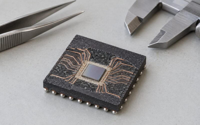
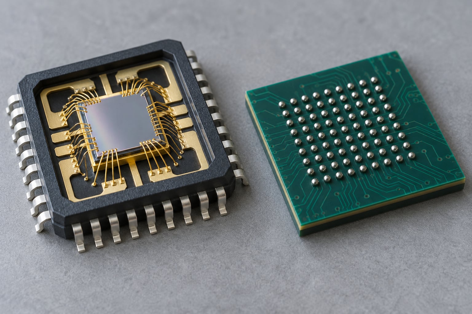
Wire bonding connects a die to its package with a thin metal wire soldered or welded from each bond pad to a lead on the lead frame or substrate. Flip-chip bonding turns the die face down and attaches it straight to the substrate with a full area array of solder bumps, so the interconnect is short, dense and arrayed instead of a perimeter loop.
Quick answer: Wire bonding for cost-sensitive, low-to-moderate I/O, mature-node parts and any device where rework and simplicity matter. Flip chip for high I/O density, high-speed signalling, low thermal resistance and small die that need big packages. Hybrid copper bonding sits above both when pitch drops below roughly 10 microns.
I have watched this decision get made badly more often than I would like, usually because it was framed as a cost argument when the real constraint was pad pitch. Below is the comparison I would put in front of a design review.
Table of Contents
- Wire Bonding vs Flip Chip Packaging at a Glance
- Electrical and Thermal Performance
- Assembly Process and Equipment
- What Is Wire Bonding?
- What Is Flip-Chip Bonding?
- Package Density and Form Factor
- Reliability, Testing, and Failure Modes
- Cost and Supply-Chain Considerations
- Wire Bonding vs Flip Chip Packaging: Common Design Tradeoffs
- Which Should You Choose?
- Frequently Asked Questions
- Is wire bonding cheaper than flip chip packaging?
- Which package has better electrical performance?
- Can wire bonding be used for high-pin-count ICs?
- What is the main disadvantage of flip chip packaging?
- Does flip chip require a more complex PCB?
- How do engineers choose between wire bonding and flip chip?
- Conclusion
Wire Bonding vs Flip Chip Packaging at a Glance
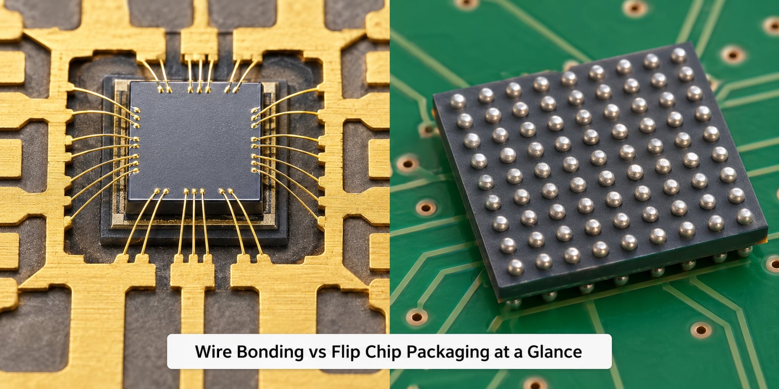
This is the head-to-head in one place. Every number below is a typical production range rather than a theoretical best case.
| Criterion | Wire bonding | Flip chip |
|---|---|---|
| Interconnect method | Metal wire loop from die pad to lead, one connection per pad | Solder bump or copper pillar on every die pad, reflowed as a mass operation |
| Typical interconnect length | 2 mm to 10 mm depending on loop height and package size | 50 to 100 microns of bump height plus a short substrate path |
| Connection style | Perimeter only | Full area array |
| Typical pitch | 75 to 150 microns on the die pad; 50 to 100 microns is achievable | 150 to 250 microns for standard bumps; 50 to 100 microns for C4 and fine-pitch work |
| Practical I/O ceiling per die | A few hundred to roughly 1,000 on a large die with multi-row layouts | Several thousand, limited by bump pitch and wafer defect density |
| Electrical parasitics | Noticeable loop inductance and wire resistance, wire loop height adds area | Very low series resistance and inductance, short return path |
| Thermal path | Die to lead frame through the attach plus wire conduction; wires also move heat sideways | Direct vertical path from die to substrate; bumps carry heat as well as signal |
| Package height | Typically 1.0 mm to 2.5 mm including the loop and cap | Under 1.0 mm is common |
| Assembly complexity | One bonder, wire spools, bond-then-cut cycles | Flip, align, mass reflow, underfill dispense and cure |
| Inspection | AOI plus wire pull and ball shear destructive tests | AOI plus X-ray for voiding, continuity and joint inspection |
| Rework | Simple to re-bond with heat | Difficult and often uneconomic once underfill cures |
| Relative cost driver | Wire, bonder time, lead frame | Bumped wafer, substrate, reflow, underfill, X-ray time |
| Strongest applications | Analog, power, automotive, RF, LED, mature-node logic | CPUs, GPUs, accelerators, network ASICs, fine-pitch RF and photonics |
Read the table as a set of trade-offs, not a scorecard. Flip chip wins every row in the top half, and it is also the more expensive, less reworkable process with a harder inspection requirement.
Electrical and Thermal Performance
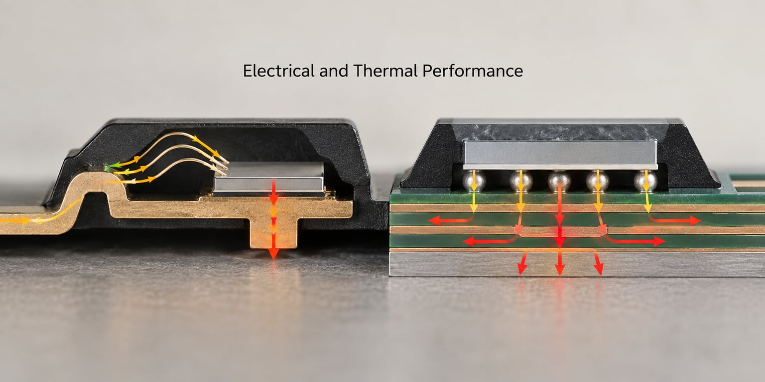
Flip chip has the better electrical performance, and the reason is geometry rather than materials. A wire bond adds 2 mm to 10 mm of conductor between the die and the substrate, and that length carries resistance and inductance that grow with every signal edge. A flip-chip bump is 50 to 100 microns tall, so the parasitic values shrink by two to three orders of magnitude.
That matters most on fast edges. When the signal rate pushes the interconnect into the regime where inductance dominates, wire loop height and loop shape set your ringing and your crosstalk budget. Flip chip pushes the interconnect inductance down far enough that the substrate and the package start to dominate instead, which is a much easier problem to design around.
Current capacity is a separate axis and it favours wire bonding in high-power parts, not the other way round. A 15 micron gold wire is a fine signal conductor but a poor power path; power modules routinely use 300 micron to 500 micron aluminum or heavy copper wire because only that gauge survives the amps involved.
| Wire diameter | Typical use | Approximate current capability | Pad pitch it supports |
|---|---|---|---|
| 15 to 20 microns, gold | RF and microwave signal, small pads | Below 0.2 A continuous | 50 micron pads |
| 25 to 30 microns, gold | General signal and low-current I/O | Roughly 0.5 A continuous | 75 micron pads |
| 75 to 100 microns, gold | Power delivery and heavier busses | Roughly 1 A to 2 A | 150 micron pads |
| 300 to 500 microns, aluminum | IGBT and power module interconnects | Tens of amps | Power pads, not fine pitch |
Current capability scales with wire diameter and with bond length, so treat those figures as ordering guidance and check them against your own thermal and bond pull data.
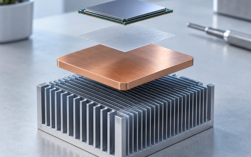
Thermally, flip chip routes heat straight down through the bumps into the substrate, which is why designers stack copper and add thermal vias under it. Wire bonding puts a wire between the die and the lead, so the heat splits between the attach path and the wire itself, and the wire also spreads heat sideways across the die edge. For a low-wattage part that difference does not matter. For a compute die pulling serious power it decides the package.
One practical note from the packaging world: moving a design from wire bond to flip chip does not automatically improve its thermal behaviour. If the new substrate has no thermal relief and the board under it has no thermal vias, the better bump geometry buys very little. Thermal relief is a die attach and lead frame design question, and the pad geometry on the board matters more than the interconnect type.
Assembly Process and Equipment
Wire bonding is a sequential, mechanical process. A wire is fed from a spool through a capillary, formed into a ball or held under a wedge, and joined to the die pad and then to the lead. The join happens through ultrasonic scrub with heat, with no liquid-phase solder involved.
What Is Wire Bonding?
Wire bonding joins the die to its package with a thin gold, copper or aluminum wire, one wire per pad. It has been the workhorse of the industry for decades and still handles the majority of devices shipped.
- Surface preparation. The die and the lead or substrate are cleaned and, in many flows, plasma treated so the pad surface is ready to bond.
- Parameter setup. Bond force, ultrasonic power, time and stage temperature are set for the wire gauge and pad metallurgy.
- First bond on the die. For ball bonding, a free air ball is formed from the wire tail and pressed into the die bond pad with ultrasonic energy. For wedge bonding, a fine wire is clamped against the pad under the wedge tool.
- Wire loop formation. The bonder tool moves to the lead or substrate pad, paying out wire and forming the loop. Loop height is set here and drives the package profile.
- Second bond. The wire is bonded to the lead, and the tail is broken off by the tool.
- Inspection and test. The loops are imaged optically and the joints are qualified by wire pull or ball shear testing.
Equipment for this step comes mainly from Kulicke and Soffa, ASMPT, Palomar Technologies and Shinkawa. The economics are dominated by bonder throughput and wire consumption, not by exotic materials.
What Is Flip-Chip Bonding?
Flip-chip bonding flips the die face down and mounts it directly on the substrate, so the bumps sit between the die and the board rather than wires arcing out to the perimeter. It removes the loop, shortens the path and lets you use the whole die face for connections.
- Wafer bumping and UBM. Underbump metallization is deposited on the pads, then a solder composition such as SnAgCu is deposited and reflowed to form bumps. Large die often use copper pillars with solder caps instead.
- Flip and align. The bumped die is picked, flipped and aligned to the substrate land pattern. Fine-pitch work uses a high-accuracy die bonder for this step.
- Mass reflow. The assembly goes through a reflow profile that melts every bump at once, which is why the bumps have to be coplanar to begin with.
- Underfill dispense and cure. For fine-pitch or high-strain applications a capillary underfill is dispensed at the die edge and drawn in by capillary action, then cured. It fills the gap, ties the die to the substrate mechanically and spreads shear stress away from the joints.
- Inspection. X-ray looks for voids, shorts and open joints that optical inspection cannot reach.
Flip-chip equipment is led by ASMPT and Besi, with Kulicke and Soffa covering a large share of mainstream die attach. The large flip-chip and advanced packaging houses are ASE, Amkor, JCET, TSMC, Samsung and Intel, which pioneered the C4 bump.
The practical difference between the two flows is speed. Wire bonding connects one pad at a time, so a 500-pad part is 500 bond cycles. Flip-chip attachment is one placement and one reflow pass, no matter how many bumps are on the die, which is exactly why flip chip wins on cost once the die is large and the pad count is high.
Package Density and Form Factor
Wire bonding is a perimeter technology, so I/O density is capped by how finely you can place pads around the die edge and how many rows you can stack there. Flip chip is an area array, so the same die face that carries a single loop of connections can carry the entire pad field.
Pitch is where the two separate cleanly. Wire bond pads sit at roughly 75 to 150 microns, with 50 to 100 micron work possible at the limit. Standard flip-chip bumps land at 150 to 250 microns. C4 bumps, developed at IBM, push that to roughly 50 to 100 microns, and copper-to-copper hybrid bonding gets to around 5 to 10 microns.
That gap drives the package size decision. When die size outgrows the perimeter limit, wire bonding needs a bigger package and longer wires to fit the connections around the edge, and the extra loop length costs you electrical performance as well as board area. Flip chip has no such ceiling, which is why processors, GPUs and AI accelerators are flip chip as a default.
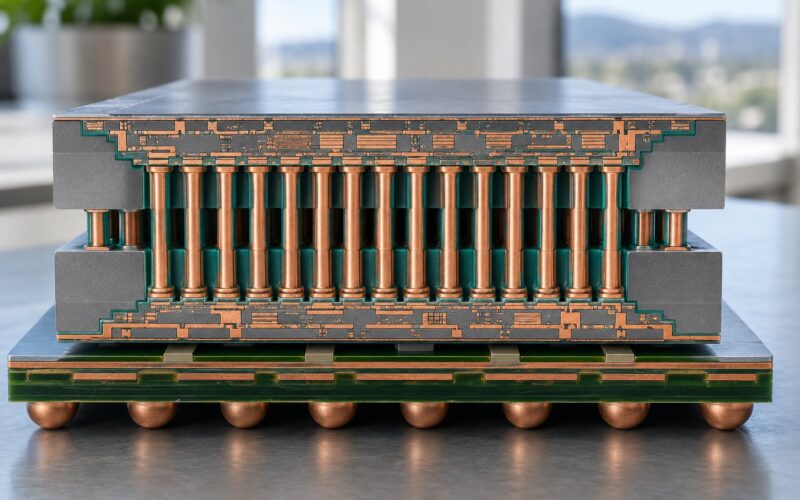
Stacked memory is the clearest illustration. DDR and HBM builds place die on die, and vertical interconnect height, not perimeter room, is the constraint. Wire bonding can be used for the logic-to-memory connections in some hybrid stacks, but the short vertical bump path is what makes the stack heights work.
Reliability, Testing, and Failure Modes
Both technologies fail, and they fail in different ways. Knowing the mechanism tells you which one your mechanical and thermal design has to defend against.
| Failure mode | Affects | Typical symptom | Mitigation |
|---|---|---|---|
| Bond lift | Wire bond | Intermittent or open joint, usually after temperature cycling | Tighter process control, larger pad geometry, suitable attach film |
| Wire break or wire sweep | Wire bond | Short to a neighbouring wire or full open, often after handling or board flex | Lower loop height, better strain relief, protect the package during handling |
| Purple plague and intermetallic growth | Gold wire on aluminium pad | Brittle joint, resistance drift, premature bond failure | Barrier metals on the pad or use of copper and aluminium wire |
| Electromigration | Both, more often on long thin wire | Voiding and open circuits over time at elevated current | Shorter and thicker conductors, current derating, cooler junctions |
| Solder joint fatigue | Flip chip | Cracked solder, intermittent failures after thermal cycling | Underfill, stiffer substrate, softer or higher-strain solder, lower CTE mismatch |
| CTE mismatch and warpage | Flip chip, especially on organic substrate | Delamination or cracked joints on large packages | Organic substrate versus ceramic choice, underfill, control of the reflow profile |
| Bump voiding and coplanarity | Flip chip | Open joints that show up on X-ray or in test | Wafer-level coplanarity control, reflow profile development, X-ray screening |
The coefficient of thermal expansion mismatch between a silicon die and an organic substrate is the root cause of most flip-chip fatigue. Silicon expands far less than the laminate does over temperature, so the joints take shear every cycle, and an underfill carries that shear away from the solder.
Ceramic substrates behave much better here, and engineers report noticeably better thermal cycling survival on ceramic than on organic laminate or FR-4. That reliability difference is one reason automotive and aerospace parts accept the cost of ceramic flip-chip.
Test methods differ because the joints differ. Wire bonding is qualified destructively with wire pull and ball shear tests, plus optical inspection of loop shape and placement. Flip chip relies on X-ray for voiding and continuity, since a good-looking bump edge tells you very little about what happened inside it. A common misconception in the industry is that visual inspection proves joint integrity; it does not, for either technology.
Cost and Supply-Chain Considerations
Neither technology is simply cheaper. What changes is which cost dominates, and the ranking flips as the package grows.
A wire-bonded package pays for the die attach material, wire and a lead frame. Flip chip pays for a bumped wafer, a multilayer organic or ceramic substrate, reflow time, possible underfill and X-ray inspection. On a small die with few pads, the substrate and bump costs outweigh any process saving, and wire bonding wins comfortably.
The crossover is documented in the IEEE cost literature. Work comparing flip chip against gold and copper wire bond packaging found that both gold and copper wire bond hold a clear cost advantage below roughly 19 mm by 19 mm packages. Once the package reaches about 31 mm by 31 mm or larger, the advantage reverses and flip chip is cheaper, because the large-area substrate cost is amortised against an interconnect that is far more efficient.
That single number is the most useful thing in this article for a cost discussion. If your part is small, do not argue about flip chip savings. If your part is large and pad-heavy, the wire bonded option is likely costing you more than you think, and the bump wafer plus substrate route usually wins on both cost and performance.
Volume and capacity push the same direction. Wire bond capacity is broad and cheap, with multiple OSATs offering it and bonders available from several vendors. Flip-chip capacity is narrower and concentrated in advanced packaging lines, so it competes for the same equipment as high-bandwidth memory and chiplet work. If your forecast ramps quickly, check where the substrate and bump wafer supply actually sits before committing.
Wire Bonding vs Flip Chip Packaging: Common Design Tradeoffs
A few patterns cover most of the parts I have seen go through this decision.
- Cost-driven legacy and analog parts. Wire bonding. Mature nodes, low I/O and long product lifecycles favour the cheapest assembly that meets the electrical need.
- High-performance processors and accelerators. Flip chip. Thousands of I/O at multi-gigahertz edge rates leave no room for loop inductance or perimeter limits.
- RF and microwave designs. Usually wire bond, often gold at 15 to 20 microns. Short, low-inductance connections to a tuned substrate still matter more than raw density, unless the design needs very fine pitch.
- Automotive and harsh-environment parts. Both, with the substrate doing the work. Ceramic flip chip survives thermal cycling better; wire bond on a robust lead frame survives handling and vibration well and stays repairable.
- Power modules. Wire bond with heavy aluminum or copper. Nothing in bump technology handles hundreds of amps with the same simplicity.
- Fine-pitch optical and photonics parts. Flip chip, often C4 or hybrid bonding, where sub-100 micron alignment is the whole point of the package.
One real case is worth mentioning: multi-chip modules that combine both. A module can wire bond a low-cost logic die to a lead frame while attaching a small RF die flip chip right next to it. The paper literature on these hybrid assemblies shows the practical result is a shorter connection for the RF path without paying bump costs across the whole module.
Where does hybrid bonding fit? Copper-to-copper hybrid bonding removes solder entirely by diffusion bonding oxide-free copper surfaces at fine pitch, typically under 10 microns. It is not yet a mainstream volume technology, but it is the direction of travel for 3D stacking and chiplet-era packaging, and it competes with flip chip rather than with wire bonding.
Which Should You Choose?
Work down this list in order and the answer usually falls out before you finish.
- Count the I/O and check the die edge. If your pad ring cannot hold the required count at a manufacturable pitch, wire bonding is not available. Go flip chip.
- Check the edge rate. Above roughly a gigahertz class of signals, interconnect parasitics start setting your timing budget. Flip chip.
- Set the thermal load. High power through a small package with no copper heat path available means flip chip. Moderate power with a lead frame design that already works means wire bond.
- Look at the environment. Wide temperature swings and thermal cycling point to flip chip on ceramic with underfill. Shock and vibration with a repairable assembly point to wire bond.
- Measure the cost crossover. Below roughly 19 mm packages wire bond is cheaper. At 31 mm and above, flip chip is generally cheaper. In between, get real numbers from your packaging house.
- Check the assembly flow downstream. Can your EMS partner handle reflow, underfill and X-ray at the volume you need? If not, the cheapest package on paper may not be buildable.
Then take the choice to a packaging provider with the actual die. Pin count, die size, thermal load, target volume and end environment are enough for a useful first answer, and they will tell you which of the crossover numbers applies to your part.
Frequently Asked Questions
Is wire bonding cheaper than flip chip packaging?
Usually yes on smaller parts, and the crossover is documented. IEEE work on flip chip versus gold and copper wire bond found wire bond holding a clear cost advantage below roughly 19 mm by 19 mm packages, with the advantage reversing once packages reach about 31 mm by 31 mm. Below that line you pay less for a lead frame and wire than for a bumped wafer and multilayer substrate.
Which package has better electrical performance?
Flip chip, clearly. A solder bump is 50 to 100 microns tall, while a wire loop typically adds 2 mm to 10 mm of conductor. That shorter path cuts series resistance and inductance by two to three orders of magnitude, which is why processors and accelerators use flip chip for high-speed links. Wire bonding stays competitive at low frequencies and short signal runs.
Can wire bonding be used for high-pin-count ICs?
Up to a point. Wire bonding is a perimeter technology, so realistic designs run from a few hundred to roughly 1,000 pads depending on die size and how many pad rows you can stack around the edge. Beyond that the package outgrows the die and the wires get longer and more expensive. Above roughly 1,000 high-speed I/O, flip chip is the normal answer.
What is the main disadvantage of flip chip packaging?
Cost and reworkability at small package sizes, plus harder inspection. You pay for wafer bumping, a multilayer substrate, reflow and underfill, and a populated flip-chip package with cured underfill is difficult to rework. Inspection also needs X-ray, since visual inspection cannot show voids inside a solder joint. Package size also brings coefficient of thermal expansion mismatch and warpage risk.
Does flip chip require a more complex PCB?
It depends on where the flip chip sits. A flip-chip BGA on a standard multilayer board needs careful solder mask and pad design, fine routing for escape, and often via-in-pad thermal relief on high-power parts. Flip chip on a wafer-level package or die-to-die inside a package does not touch the PCB at all. The board complexity depends on how the package is assembled, not on the interconnect alone.
How do engineers choose between wire bonding and flip chip?
Start with the binding constraint: pad count and die size set the density limit, edge rate sets the electrical limit, power dissipation and the available heat path set the thermal limit, and the end environment sets the reliability limit. Only then look at cost, and use the roughly 19 mm and 31 mm package crossover figures as a starting point rather than a quote. Finally confirm that your packaging house and assembly partner can build the volume you need.
Conclusion
Start with I/O density, because it is the one constraint that can eliminate wire bonding outright. If the pad ring does not fit at a manufacturable pitch, the decision is made for you. Then check electrical performance against your edge rate, thermal load against your available heat path, and the reliability environment against your temperature range and shock levels.
Only after those four checks does cost matter, and then use the package size as your guide: wire bonding holds the advantage below roughly 19 mm, flip chip takes it from roughly 31 mm up. Bring die size, pad count, power and annual volume to a packaging provider and ask them to model both options. A wire bonding vs flip chip packaging decision made on documentation alone usually goes wrong somewhere in the middle, where the datasheets stop talking.