Short answer: 2.5D packaging puts two or more separately made chip dies next to each other on a thin shared silicon interposer, using very fine-pitch connections between them, instead of stacking them vertically the way 3D packaging does. The dies then behave like one large chip.
If you have read a spec sheet for an AI accelerator or a high-end GPU and wondered how one part carries several gigabytes of memory at that speed, this is the technology behind it. It also explains why an H100 or an MI300 is not just a bigger chip.
I’ll walk through what the label means, what the interposer actually does, how it differs from 2D and 3D, and what it costs in yield, heat and test. No vendor pitch, just the engineering.
Table of Contents
- What 2.5D Packaging Means in Chips
- Why the label says 2.5D
- The reticle limit is the real driver
- 2.5D Packaging vs 3D Packaging: What Is the Difference?
- How Does 2.5D Chip Packaging Work?
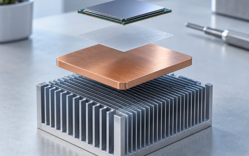
- What Are the Main Parts of a 2.5D Package?
- How Is a 2.5D Package Manufactured and Assembled?
- Why Does 2.5D Packaging Matter for Chip Performance?
- Interposer materials compared
- Where Is 2.5D Packaging Used in Modern Electronics?
- Named commercial implementations
- What Are the Main Challenges of 2.5D Packaging?
- Is 2.5D Packaging the Same as a Multi-Chip Module?
- How Do You Know Which Packaging Approach to Choose?
- Frequently Asked Questions
- Is 2.5D packaging the same as 3D chip stacking?
- Why do AI processors use 2.5D packaging with HBM?
- Does 2.5D packaging always use a silicon interposer?
- What is hybrid bonding, and is it required for 2.5D packaging?
- Why is 2.5D packaging more expensive and harder to yield than conventional packaging?
- Conclusion
What 2.5D Packaging Means in Chips
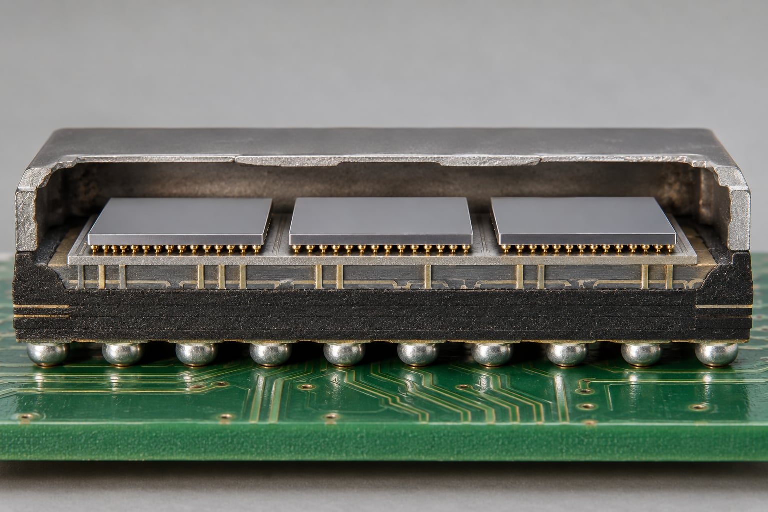
2.5D packaging is an advanced semiconductor packaging method that places two or more active dies side by side on a thin silicon interposer, joined by very fine microbumps. The interposer routes those connections down to the package substrate and out to the board, so the dies act as one chip with far shorter, faster and more efficient links than a conventional substrate allows.
That is the whole idea in two sentences. The part you buy is still a package sitting on a printed circuit board. What changed is the wiring inside it.
Why the label says 2.5D
The name is a compromise, and a slightly awkward one. A monolithic die on its own substrate is 2D integration. Dies stacked vertically with through-silicon vias are 3D. 2.5D sits between the two: full 3D vertical density in the connections between dies, but no vertical transistor stacking.
Engineers use the term loosely. You will see it applied to fan-out packages and to some silicon-bridge designs that a strict reading would call something else entirely. Treat it as a family resemblance rather than a spec.
The reticle limit is the real driver
A lithography reticle caps how large one die can be printed, and that ceiling has not moved much in years. Beyond roughly 800 to 850 square millimetres for a leading-edge reticle area, you cannot simply make a bigger monolithic die.
That single physical fact pushed vendors to partition large chips into smaller dies and reconnect them inside the package. Side-by-side placement was the easiest way to do it with tools and processes that already existed. So 2.5D packaging is not a speculative idea. It is the direct consequence of hitting the size limit and needing performance to keep climbing anyway.
2.5D Packaging vs 3D Packaging: What Is the Difference?
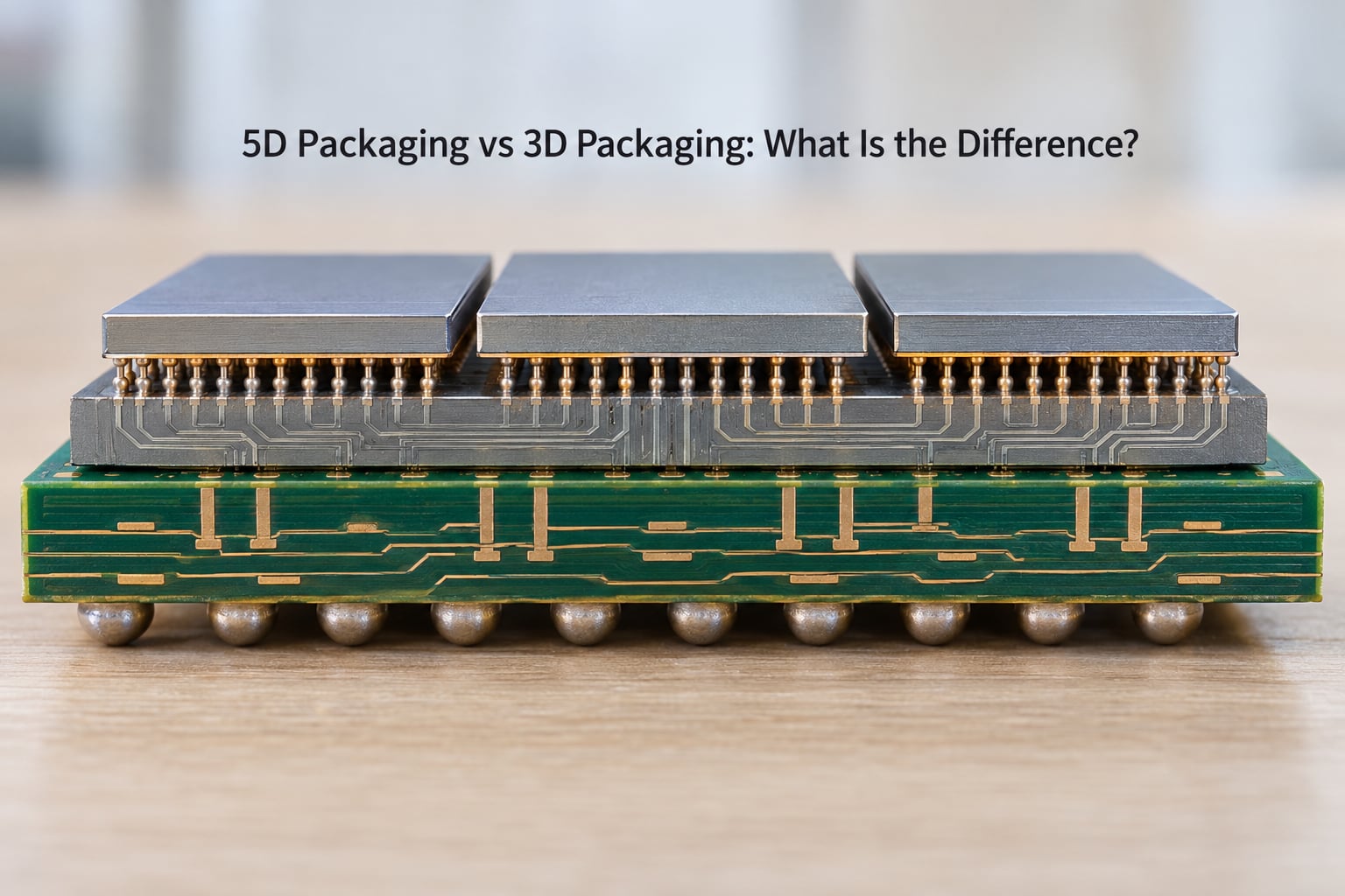
The clearest way to see the difference is to look at where the dies sit relative to each other and what links them. Both approaches put dies in one package, but one is lateral and the other is vertical.
| Factor | 2D (monolithic) | 2.5D | 3D |
|---|---|---|---|
| Die placement | One die per package | Multiple dies side by side, same plane | Dies stacked vertically on top of each other |
| Die-to-die link | None needed | Microbumps or hybrid bonds onto a shared interposer | Microbumps or hybrid bonds through vias in the stack |
| Routing density between dies | Not applicable | Silicon-class line and space rules, very fine | Highest density, shortest vertical links |
| Interconnect length | Longest, dies far apart on the board | Millimetres | Micrometres to a millimetre |
| Thermal complexity | Simple, one heat path | Hard, hotspots spread sideways | Hardest, heat funnels straight through the stack |
| Manufacturing complexity | Standard | Alignment, RDL and substrate complexity | Adds wafer bonding and very tight thermal budgets |
| Cost | Lowest | Higher than 2D, cheaper than full 3D | Highest, with hard capacity limits |
| Repairability | Not possible | Essentially none once assembled | Essentially none, sometimes worse |
| Good fit | Cost-sensitive parts, analog-heavy designs, small MCUs | AI accelerators, GPUs with HBM, networking ASICs, HPC nodes | Logic-on-logic stacking where a single extra process step is worth it |
The practical takeaway is that 2.5D gives you most of the bandwidth benefit of 3D while staying on processes that are already manufacturable in volume. Vertically stacked logic also has a thermal problem that side-by-side dies avoid, because heat at least has somewhere sideways to go.
3D wins on raw interconnect density. 2.5D wins on yield, cost and the ability to mix process nodes, which is why most shipping AI silicon uses it.
How Does 2.5D Chip Packaging Work?
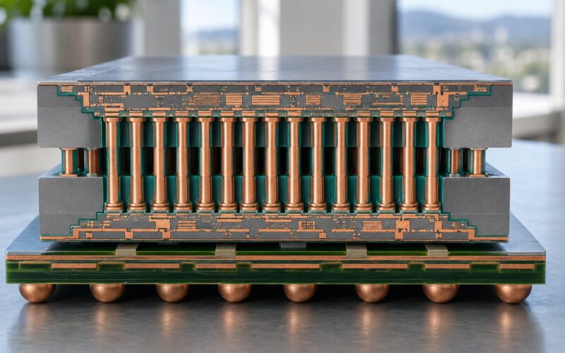
The signal path runs from a transistor in one die, through a micro-bump array into the interposer, across its redistribution layer, down through the interposer’s vias into the package substrate, and out to the board. Each hop adds parasitic resistance, capacitance and latency, so the whole point of the interposer is to remove hops rather than to add them.
Follow the data moving out of an AI accelerator’s compute die toward its memory stacks. It crosses maybe a few millimetres of silicon and a micro-bump array, nowhere near the centimetre-plus of board trace that a conventional multi-chip module would force it to travel. Shorter path, lower capacitance, less energy per bit.
What Are the Main Parts of a 2.5D Package?
Not every design contains every component below. The list is the common denominator, and which pieces appear depends on the architecture.
- Compute dies. The active logic. Often several, sometimes built on different process nodes for different jobs.
- I/O, cache or specialty dies. Serdes, PHY, security controllers, analog blocks, or an I/O die fabricated on a mature node that is cheaper and more robust than leading-edge logic.
- Memory stacks. HBM sits beside the compute die, built as a vertical stack of memory dies connected by through-silicon vias and joined to the interposer with microbumps.
- Microbumps. Solder balls roughly 25 to 60 micrometres in diameter that form the physical and electrical bond between die and interposer.
- The interposer and its redistribution layer. A thin silicon die carrying metal routing layers, with through-silicon vias passing signals from the top face down to the bottom. This is the expensive, precision part.
- Package substrate. An organic or glass build-up laminate that takes signals from the interposer out to the board at a much coarser pitch.
- Heat spreading hardware. A lid or heat spreader bonded to the package, often the most visible thermal constraint in the whole stack.
- The power delivery network. Decoupling capacitors and power distribution, increasingly embedded on the interposer itself because the currents are large and fast.
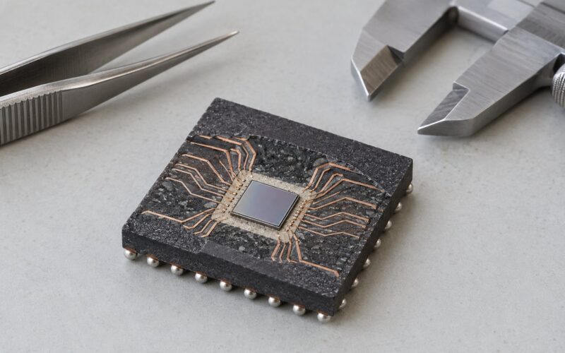
Silicon bridges are a related part. Intel’s EMIB embeds small silicon bridge dies into the organic substrate rather than using a full interposer, which keeps cost down when the dies are small.
How Is a 2.5D Package Manufactured and Assembled?
The generic sequence looks the same across vendors, even where the details differ.
- Wafer fabrication. Each die type is made separately, on whatever node suits it best.
- Known-good-die test. Dies are probed at wafer level and bad ones binned before any of them are combined. This is the step that makes the whole economics work.
- Interposer preparation. Redistribution layers are built on the interposer wafer, with fine-pitch metal routing and through-silicon vias.
- Bump formation. Microbumps are deposited on interposer and die pads. At the densest pitches, copper pillars or hybrid bonding take over.
- Die alignment and attach. A pick-and-place machine places dies at micron accuracy, then reflow or thermocompression bonds them.
- Package assembly. The interposer assembly is mounted on the package substrate, and the lid and heat spreader go on.
- Inspection. X-ray, acoustic and optical methods look for voids, missing bumps and delamination, since none of these can be fixed later.
- Final electrical and thermal test. The completed package is tested as a whole, then characterised for thermal resistance and binned.
Yield is the pressure behind every one of those steps. Combine four dies and a large interposer, and the probability that all five are good falls off fast. Known-good-die screening at wafer level exists precisely to keep that multiplication from destroying the yield of the finished part.
Interposers can also be built as large panels rather than whole wafers, which is one of the industry’s answers to the cost and size ceiling. The hard part is not making a big interposer. It is making one with no defects across its whole area.
Why Does 2.5D Packaging Matter for Chip Performance?
The benefits are not abstract. Each one shows up in a specific place in a workload.
- Shorter, denser communication paths. Die-to-die links on a silicon interposer run at fine pitch, so thousands of connections fit between two neighbouring dies. For an AI accelerator, that turns memory access from a bottleneck into a background task.
- Higher aggregate bandwidth. Several HBM stacks surround the compute die, and the interposer can feed them all at once. This is the single biggest reason AI parts look the way they do.
- Lower energy per bit. This is the one engineers underrate. Moving data off-chip costs far more energy than computing on it. Short links mean less power spent on moving weights and activations.
- Modular use of process nodes. A compute die on a leading node, I/O on a mature node, HBM on its own process. Each block uses the process that suits it, which lowers cost and can improve reliability.
- Yield recovery from smaller dies. A 700 square millimetre die at 99% yield is a poor bet. Four 175 square millimetre dies at the same per-die yield are far more likely to all pass. This is why chiplet partitioning raised output as much as it raised flexibility.
- Reuse of proven chiplets. A die qualified in one product generation can carry into the next. For networking and FPGA vendors this shortens new-product schedules considerably.
Take an AI accelerator as the concrete case. Its arithmetic units would sit idle waiting on weights if memory could not keep up. Putting HBM within millimetres on a shared interposer raises effective system bandwidth enough that the compute becomes the limit again, which is the only place you want the bottleneck.
Interposer materials compared
The interposer is the part that decides cost and density, and there are three real options.
| Material | Routing pitch | Cost | Flatness and warpage | Where it fits |
|---|---|---|---|---|
| Silicon | Finest, sub-micron line and space | Highest, and the wafer is a single large reticle | Excellent flatness, matched CTE to the dies | Leading-edge AI and HPC packages with HBM |
| Organic | Coarser, but improving with build-up layers | Lowest | More prone to warpage as layer count rises | Cost-sensitive modules, mid-range silicon bridge designs |
| Glass | Fine, with excellent dimensional stability | Promising, not yet mainstream | Very flat, low warpage, tunable coefficient of expansion | Emerging large-package and future panel work |
Glass is interesting because it is flat and dimensionally stable, which matters when the package is large and the layers are thin. It also happens to be a decent optical waveguide, which makes it a candidate for co-packaged optics later on.
Where Is 2.5D Packaging Used in Modern Electronics?
Applications follow one rule: use it when the design has a bandwidth problem that a board-level connection cannot solve.
- AI accelerators and GPUs. Compute die or dies plus several HBM stacks. This is the flagship case, and the reason advanced packaging capacity became a strategic constraint.
- High-performance computing. Exascale-class nodes need very high aggregate memory bandwidth per socket, which is exactly what interposer integration delivers.
- Networking and switch silicon. Serdes and I/O placed next to switching logic on mature nodes, with reusable chiplets across product generations.
- FPGAs. Wide, heterogeneous devices with logic, memory and hard processor cores built from separate dies.
- Large-format semiconductor IP. Wide I/O dies paired with logic on a bridge, extending reach without forcing a huge reticle-limited die.
- RF and photonics integration. Compound semiconductor and silicon photonics dies mounted alongside CMOS logic, which is heterogeneous integration in its clearest form.
Named commercial implementations
| Technology | Vendor | Approach | Notably used in |
|---|---|---|---|
| CoWoS-S, CoWoS-R, CoWoS-L | TSMC | Silicon interposer between compute and HBM; L adds a local silicon interconnect for very dense die-to-die | NVIDIA A100, H100, H200; many AI accelerators |
| SoIC | TSMC | Hybrid-bonded 3D stacking, front and back side | 3D logic-on-logic products |
| InFO | TSMC | Fan-out packaging without a substrate between die and board | Mobile application processors |
| EMIB | Intel | Silicon bridge dies embedded in the organic substrate instead of a full interposer | Intel Ponte Vecchio |
| Foveros and Foveros Direct | Intel | 3D stacking, including direct copper bonding for logic to logic | Intel client and data centre parts |
| X-Cube | Samsung | Hybrid-bonded 3D and 2.5D integration | Exynos-class parts, 3D V-Cache style stacking |
| FOCoS-Bridge | ASE | High-density fan-out bridging dies without a full silicon interposer | Volume 2.5D and HBM integration |
If you want to see the concept in hardware you might own, the clearest shipped examples are NVIDIA’s H100 and H200 accelerators, which use CoWoS with an accelerator die and HBM stacks on a silicon interposer. AMD’s Instinct MI300 is built the same way, with several compute tiles and HBM. Intel’s Ponte Vecchio data centre GPU uses EMIB, a different route to the same goal, and AMD’s 3D V-Cache is the contrasting vertical approach.
What Are the Main Challenges of 2.5D Packaging?
Everything above has a cost attached, and the costs are concentrated in packaging rather than in fab.
Cost and capacity. A large silicon interposer is expensive, and the equipment that builds one is not cheap to buy or to staff. Advanced packaging capacity became a real bottleneck for AI accelerators, so allocation, not design, sometimes decides when a part ships.
Interposer size. Interposers are made on wafers, which caps how large a package can get. Exceeding the limit means stitching panels together, and seams are hard. This is one reason smaller dies packed more densely beat a few very large dies.
Yield multiplication. Every additional known-good component lowers the probability that the whole package passes. Vendors counter this with wafer-level screening and by using as few dies as the design allows, but the arithmetic never goes away.
Alignment. Placement accuracy has to hold at micron scale across a package that may carry six or more dies. Miss one bump on a dense array and that die link is dead, with no rework path.
Thermal resistance. Side-by-side dies spread heat differently from a single die, and HBM in particular runs hot. Getting heat out of a package where several dies dissipate at full tilt and the lid is the only exit is the hardest physical problem here.
Power delivery. Modern AI parts draw enough current, fast enough, that the power network has to live on the interposer. On-package decoupling capacitors are one solution; the rest is a routing problem nobody fully solved.
Test coverage. Once dies are buried inside a package, probing individual nets becomes impractical. Design for test, boundary scan and additional test insertion have to be planned at architecture time, because they cannot be added afterwards.
Inspection. Non-destructive imaging of thousands of microbumps per die pair is slow and expensive, and it still only tells you the bonds exist, not that they are all sound.
Warpage. Silicon, copper, organic substrate and solder all expand at different rates. Large packages under thermal cycling can bow enough to stress the bumps.
Repairability and supply chain. A package with one bad die is scrap. That makes die sourcing, wafer allocation and second sources a coordination problem across several companies.
The honest framing: you are trading fabrication difficulty for packaging difficulty, and hoping the performance gain is worth more than the extra verification effort.
Is 2.5D Packaging the Same as a Multi-Chip Module?
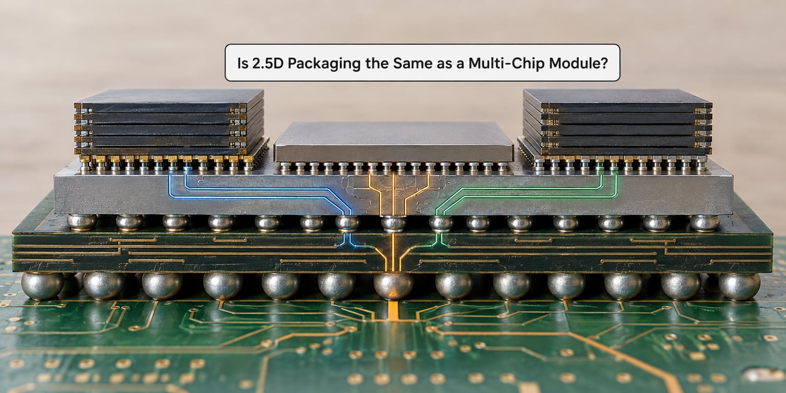
They overlap, but they are not the same thing. A multi-chip module is the general idea of putting several dies in one package. 2.5D is a specific, higher-density way of doing that.
An ordinary multi-chip module places dies on a conventional organic substrate and connects them at substrate pitch, which lands in the range of roughly 125 micrometres. That is fine for a modest sensor hub or a small microcontroller module. The wires between dies are long relative to the die itself, and bandwidth is what it is.
Add a silicon interposer with redistribution layers and microbumps, or hybrid bonds, and the connections between dies become orders of magnitude finer. Now the dies can behave like parts of one chip rather than parts sharing a shelf. That additional routing layer is the real dividing line between a module and 2.5D integration.
Terminology varies by organisation, which is why the question comes up so often on packaging forums. Some companies count silicon-bridge designs as 2.5D, others call those a module with a bridge. The useful test is not the label. It is the pitch of the connections between dies and what bandwidth that pitch can deliver.
How Do You Know Which Packaging Approach to Choose?
Work through these in order before picking an architecture.
Required bandwidth and latency. If the design is bandwidth-bound and the data has to come from memory every cycle, interposer integration is the answer. If throughput is modest, a conventional package is cheaper and simpler.
Die size and node mix. Does the design exceed the reticle limit? Will parts benefit from different process nodes? If yes to either, partitioning into chiplets has real value.
Power budget for data movement. Energy per bit spent on off-chip traffic can exceed energy spent computing. In power-limited designs this is often the deciding number.
Thermal budget. Vertical stacking funnels heat through the top die. If the design already runs hot, 2.5D gives heat a lateral escape path.
Cost and production volume. Silicon interposers carry a fixed cost that only makes sense at volume. A low-volume, low-cost part rarely justifies one.
Test strategy. Every additional die is another known-good-die dependency and another test insertion problem. Budget for it from the start.
As a rough decision: stay 2D for cost-sensitive, analog-heavy or small parts where the reticle limit is not close. Use a multi-chip module when dies can share a substrate and bandwidth is not critical. Choose 2.5D when bandwidth and energy per bit dominate the design. Reach for 3D stacking when interconnect density matters more than thermal headroom.
Frequently Asked Questions
Is 2.5D packaging the same as 3D chip stacking?
No. Both put several dies in one package, but 2.5D places them side by side on a shared interposer, while 3D stacks them vertically with through-silicon vias. 2.5D offers most of the bandwidth benefit, keeps heat with more places to go, and stays on processes that already run at volume. 3D gives the densest, shortest interconnects, at the cost of harder thermal design and tighter manufacturing.
Why do AI processors use 2.5D packaging with HBM?
AI accelerators are usually limited by memory bandwidth, not arithmetic. Placing high bandwidth memory within millimetres of the compute die on a silicon interposer gives far more aggregate bandwidth at much lower energy per bit than a board-level connection. That keeps the compute units supplied with data, which is why nearly every shipping AI accelerator and high-end GPU uses this arrangement.
Does 2.5D packaging always use a silicon interposer?
No, though silicon is the usual choice for leading-edge parts because it allows the finest routing rules and has excellent flatness. Organic and glass interposers exist for cost-sensitive or larger-format designs, and some designs skip the full interposer by embedding small silicon bridge dies directly in the organic substrate. The shared fine-pitch routing layer is what matters, not the material.
What is hybrid bonding, and is it required for 2.5D packaging?
Hybrid bonding is a technique that joins two wafers or dies directly using embedded copper and dielectric, without solder bumps. It allows far finer pitch and lower interconnect energy than microbumping. It is not required for 2.5D packaging, which is commonly built with microbumps alone, but it is increasingly used to raise density and to build vertical stacks.
Why is 2.5D packaging more expensive and harder to yield than conventional packaging?
A finished 2.5D package combines several known-good dies, a large routing interposer, a build-up substrate and a lid, and every one of those can fail. Yield falls as components multiply, and packages cannot be reworked. Inspecting thousands of microbumps non-destructively is slow, and equipment capacity for advanced packaging is limited, which has made allocation a real constraint for AI parts.
Conclusion
What 2.5D packaging means in chips is straightforward: several separately fabricated dies placed laterally on a shared routing platform, connected by microbump or hybrid-bond interconnects, with the exact architecture varying from design to design.
Before choosing an implementation, write down five numbers: required bandwidth, power budget for data movement, thermal budget, cost ceiling, and production volume. Those five settle most of the argument. Bandwidth-bound, high-volume, leading-edge designs end up on a silicon interposer with HBM. Everything else usually does not need one.