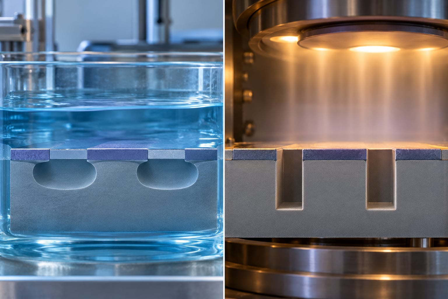
If you are specifying an etch step for a wafer process, the short version of wet etch vs dry etch in semiconductor manufacturing is this: wet etching dissolves material in a liquid bath and is hard to steer sideways, while dry etching uses a low-pressure plasma to remove material mostly straight down. Wet chemistry wins on selectivity, cost, and the absence of damage. Dry plasma wins on feature size, sidewall angle, and pattern control.
Etching is the subtractive half of pattern transfer. You coat a wafer with resist, expose and develop a pattern, then remove the film underneath so the pattern is transferred into the material you actually care about. Both wet and dry etching do that removal. They differ in what they use to do it, how precisely they can aim it, and what they leave behind on the wafer and in the fab.
This guide is written for process engineers, integration engineers, MEMS researchers, and advanced students who need the practical tradeoffs rather than textbook definitions. Last updated October 2026.
Table of Contents
- Wet Etch vs Dry Etch in Semiconductor Manufacturing at a Glance
- How Wet Etch and Dry Etch Remove Material
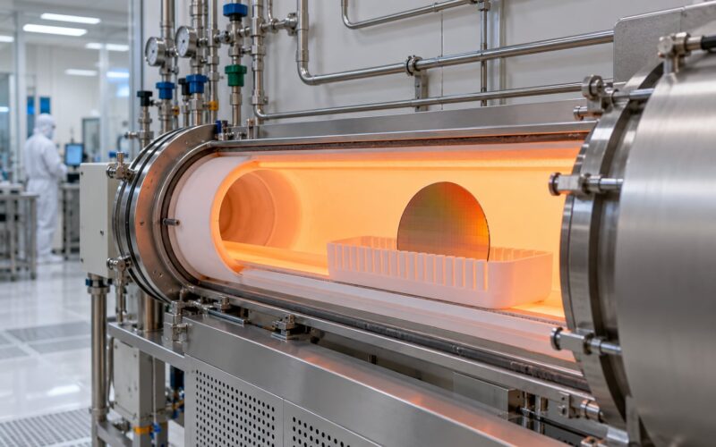
- What wet etching does: chemical dissolution in a liquid bath
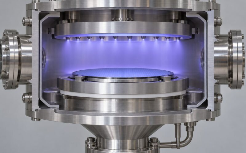
- What dry etching does: plasma, ions, and radicals
- Wet Etch vs Dry Etch in Semiconductor Manufacturing: Key Tradeoffs
- Selectivity: the number that decides most steps
- Profile control, sidewall angle, and etch bias
- Etch rate, throughput, and pattern-dependent loading
- Contamination, damage, and residue
- Conductor etch vs dielectric etch
- Wet Etch Advantages and Limitations
- Dry Etch Advantages and Limitations
- How Process Engineers Select Between Them
- Which Should You Choose?
- Frequently Asked Questions
- Is wet etch or dry etch better for semiconductor manufacturing?
- What is the main difference between wet etch and dry etch?
- Which etching method gives better sidewall control?
- Is dry etching more expensive than wet etching?
- Can wet etch and dry etch be used in the same process flow?
- What factors determine etch selectivity?
- Conclusion
Wet Etch vs Dry Etch in Semiconductor Manufacturing at a Glance
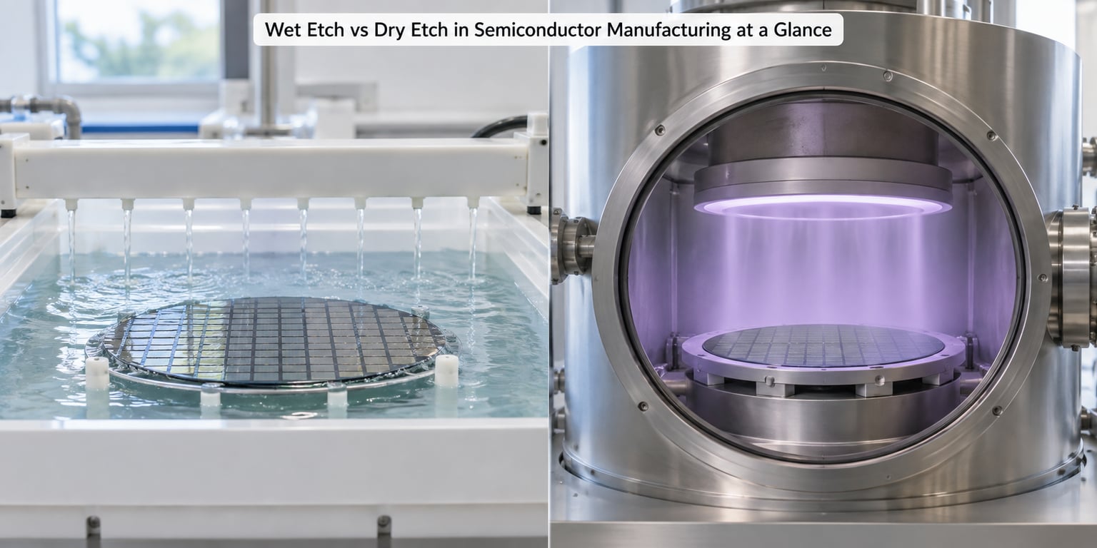
The table below is the fastest way to see the split. Every value is a typical range for a production process, not a universal rule.
| Criterion | Wet etch | Dry etch |
|---|---|---|
| Removal mechanism | Chemical dissolution in liquid | Chemical reaction plus ion bombardment in plasma |
| Etchant medium | HF, BOE, KOH, TMAH, H3PO4, HNO3 | CF4, CHF3, SF6, Cl2, HBr, BCl3, O2 |
| Typical direction | Isotropic by default; crystal-dependent with KOH and TMAH | Anisotropic by default; isotropic with XeF2 |
| Practical feature size | Above roughly 1 to 2 micrometers | Sub-micron down to tens of nanometers |
| Aspect ratio | Low, typically under 2:1 | High, 20:1 and beyond in modern structures |
| Etch rate | 0.5 to 5 micrometers per minute | 0.1 to 1 micrometer per minute |
| Selectivity | Very high, often 100:1 or better | Moderate, typically 2:1 to 10:1 |
| Substrate damage | Chemical only, no bombardment | Surface and subsurface ion damage |
| Profile control | Mask-limited, sidewalls defined by diffusion | RF-biased, near-vertical sidewalls |
| Processing mode | Batch, many wafers per bath | Single wafer per chamber |
| Endpoint control | Time or timed dips, load cells | In-situ optical emission spectroscopy |
| Mask compatibility | Photoresist, oxide, or metal hard mask | Photoresist, oxide, nitride, or metal hard mask |
| Tool complexity | Bath, heaters, filters, spin dryer | Vacuum, RF generators, gas delivery, abatement |
| Main cost driver | Chemical volume and effluent treatment | Capital cost, uptime, vacuum pumps, gas |
| Waste stream | Liquid effluent plus acid fume abatement | Gas abatement plus pump maintenance |
| Typical uses | Blanket removal, native oxide, resist undercut, release | Vias, trenches, gates, metal lines, HAR channels |
Two rows deserve a second look. Selectivity and directionality both break from what people expect, and that is where most of the interesting engineering lives.
How Wet Etch and Dry Etch Remove Material
What wet etching does: chemical dissolution in a liquid bath
In a wet etch, the wafer sits in a bath of liquid etchant, or on a spray head fed by that etchant. The exposed film reacts with the liquid, the reaction products dissolve, and the etched material leaves with the solution. A rinse in deionized water follows, then a spin or Marangoni dry.
The pattern comes from the mask. Photoresist, silicon dioxide, or a deposited metal hard mask blocks the liquid, and the chemistry does the removal everywhere the mask is open. Because liquid etchants reach the exposed film from every direction at once, the standard result is an isotropic etch: material goes down at the same rate it goes sideways, so features end up wider than the mask opening and you get undercut beneath the mask edge.
There is an important exception. Crystalline silicon etched in potassium hydroxide or tetramethylammonium hydroxide etches at different rates depending on the crystal plane facing the liquid. Fast-etching {100} and {110} planes recede quickly while slow-etching {111} planes stay behind, and the intersection of those planes produces a clean V-groove or an inverted pyramid. That is a genuinely anisotropic wet etch, and it is the backbone of bulk micromachining.
What dry etching does: plasma, ions, and radicals
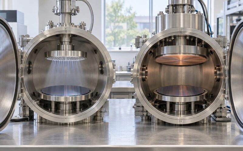
Dry etching ionizes a process gas at low pressure and lets the resulting species reach the wafer. Neutral radicals do most of the chemical work and they arrive from every direction, so on their own they behave like a slow wet etch. The directional part comes from the ions: an electric field across the chamber accelerates them so they strike the wafer roughly perpendicular to its surface.
In reactive ion etching, the wafer sits on a powered electrode, so ions are driven down into the pattern and vertical sidewalls form because the ions hit the bottom of the opening and only glance off the top of the resist. A heavier, purely physical process like sputter etching is the opposite case: it is directional but very unselective, since it removes almost anything at a similar rate.
One more counter-example belongs here. Xenon difluoride is a dry etch with no plasma at all. It reacts with silicon to form volatile products in the gas phase, so it etches deeply and isotropically with no ion bombardment. Dry does not automatically mean anisotropic, and that is worth remembering when someone tells you the two categories line up perfectly.
One reason gas has an advantage in small features comes down to transport. Gas molecules diffuse into narrow openings far more readily than liquid, so plasma chemistry keeps working when the feature is much smaller than the gap between molecules in a liquid.
Wet Etch vs Dry Etch in Semiconductor Manufacturing: Key Tradeoffs
Selectivity: the number that decides most steps
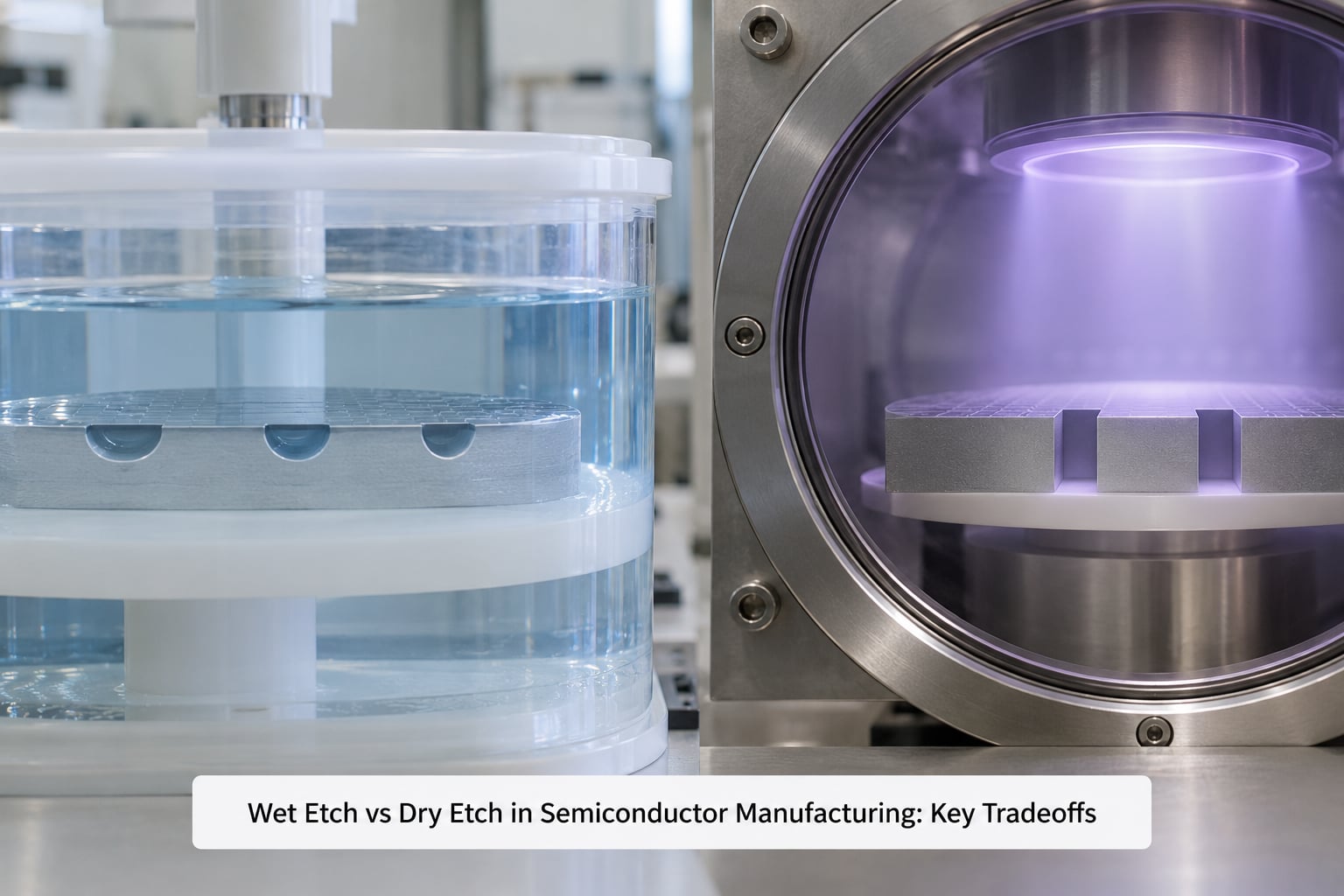
Selectivity is the ratio of the etch rate of your target film to the rate of the layer beneath it or the mask above it. Wet chemistry is the selectivity champion. Buffered oxide etch removes thermal silicon dioxide while barely touching the silicon underneath, often at 100:1 or better, which is why the pre-gate clean is a wet step in nearly every CMOS flow. Hot phosphoric acid at around 85 degrees C removes aluminum while leaving silicon dioxide essentially untouched, and KOH on silicon shows a rate difference of one to two orders of magnitude between {100} and {111} faces.
Dry etch selectivity is real but narrower, usually in the 2:1 to 10:1 range, and it depends on the gas chemistry and the plasma conditions. Fluorine-based recipes for silicon dioxide tend to sit near 1:1 against silicon because fluorine reaches both. HBr and chlorine chemistries for polysilicon and metal gates do better, sometimes above 10:1 against oxide, and end with an overetch step that stops before the stop layer goes.
Profile control, sidewall angle, and etch bias
A liquid etch gives you whatever the mask and the chemistry produce, which is normally a rounded opening with a lateral undercut proportional to the etch depth. Photoresist softens as it soaks, so a long wet etch also loses mask height and changes the feature size you started with. For a 2 micrometer deep etch, the undercut can be a full micrometer on each side, and that lateral spread is what sets your design rule for the pitch.
Plasma etch controls the profile with knobs you can turn. Chamber pressure, gas flows, source power, and bias power trade lateral etch against vertical etch, which engineers describe as a bow in the sidewall. More bias gives a straighter wall and more damage; less bias reduces damage and lets the profile bow outward. Pattern-dependent loading does the rest: a dense field of lines etches at a different local rate than an isolated line, and on a chip full of varying pattern density that shows up as a critical dimension spread across the wafer.
Etch rate, throughput, and pattern-dependent loading
The rates below are typical fab ranges and shift with concentration, temperature, mask material, and tool condition. Treat them as the order of magnitude you should expect, not as a spec.
| Process | Target material | Typical etch rate | Selectivity notes |
|---|---|---|---|
| 49 percent HF, room temperature | Thermal SiO2 | About 1 to 3 micrometers per minute | Very high against silicon; rate climbs steeply with temperature |
| Buffered oxide etch, 10:1 | Thermal SiO2 | About 0.5 to 1.5 micrometers per minute | 100:1 or better against silicon; well controlled across a bath |
| KOH or TMAH, 80 degrees C | Silicon {100} | About 1 to 2 micrometers per minute | {111} face etches 100 times slower, forming V-grooves |
| Hot phosphoric acid, 85 degrees C | Aluminum | About 1 to 2 micrometers per minute | Excellent against silicon dioxide and nitride |
| CF4 with oxygen plasma | Silicon and oxide | About 0.5 to 2 micrometers per minute | Low to moderate, chemistry dependent |
| HBr or Cl2 plasma | Polysilicon or metal | About 0.2 to 1 micrometer per minute | Better against oxide than fluorine recipes |
Dry etch is slower per wafer in raw removal rate, but throughput is not the same number. A wet bench runs a full batch of wafers in one bath, while a single-wafer plasma tool takes minutes per wafer including pumpdown and vent. For a blanket film strip, wet wins on wafers per hour. For a patterned deep trench, the dry tool’s slower rate is the only rate available.
Contamination, damage, and residue
Wet chemistry can leave watermarks, mineral residue, and stiction when fragile structures dry and capillary forces pull released layers down onto the substrate. Spin drying and vapor drying exist specifically to manage that, and a supercritical or vapor-phase step is sometimes justified when the structure cannot survive a liquid-to-vapor transition. On the contamination side, wet chemistries carry their own metals: KOH is a known source of potassium ion contamination, which is why CMOS flows prefer TMAH when a crystal-plane anisotropic etch is needed.
Dry etch introduces different problems. Energetic ions cause surface damage and a shallow subsurface defect layer in silicon, which matters for gate dielectrics, channel regions, and anything where carrier mobility is the point. Charging on insulating structures distorts the ion trajectory and produces notching at the feature base and bowing at the top. Both are addressed with the same knob, lowering bias power, which is a straight trade of profile quality for device quality.
Conductor etch vs dielectric etch
Conductor etch and dielectric etch are different jobs with different constraints, and the choice of method changes with the material. This question comes up constantly and is worth separating cleanly.
| Attribute | Conductor etch | Dielectric etch |
|---|---|---|
| Typical material | Aluminum, copper, tungsten, polysilicon | Silicon dioxide, silicon nitride, low-k dielectrics |
| Dominant method | Dry, with wet as a post-clean | Wet for blanket, dry for patterned |
| Wet chemistry option | Hot H3PO4 for aluminum, HNO3 for copper | HF and BOE for oxide |
| Mask material | Hard mask, often oxide or nitride | Photoresist is often sufficient |
| Endpoint signal | Metal-specific emission line or timed overetch | Silicon-based emission change when oxide clears |
| Dominant risk | Corrosion after wet clean, metal corrosion at vias | Residue, watermarks, pattern collapse in dense films |
Metal lines need vertical sidewalls to carry current and to survive later steps, which points to dry etch with a hard mask. Oxide and nitride, when they are being removed everywhere rather than patterned, are cheaper and cleaner to strip in a bath.
Wet Etch Advantages and Limitations
Wet etching is the cheaper tool per wafer and the simpler one to run. A bench, a heated tank, a filter, and a spin dryer handle a whole batch, and the consumable is just chemical volume plus effluent treatment.
Its strengths show up in specific steps. Blanket removal of oxides, nitrides, and sacrificial films is fast, with rates several times higher than plasma. Selectivity against the layer below is the best available, which is why the last clean before a gate stack is a wet dip. There is no ion bombardment, so no subsurface damage, no charging, and no notching, and released MEMS structures come out intact because nothing struck them.
Crystal-plane etching with KOH or TMAH gives anisotropic wet profiles on a simple bath, which is how V-grooves and inverted pyramids are formed for MEMS diaphragms and through-wafer inlets. Undercut and release steps are also natural in liquid, since the etchant reaches beneath the mask on all sides without any extra hardware. And GaAs and InP optoelectronic layers are often processed wet because the chemistry is well understood and the selectivity is clean.
The limits are just as concrete. Undercut scales with depth, so a deep wet etch destroys the feature spacing you designed, and above roughly 1 to 2 micrometers of critical dimension, wet etch stops being practical. Microloading inside dense patterns changes the local rate and shrinks features unpredictably. Photoresist soaks, swells, and loses its profile during long exposures to hot liquid, which forces a hard mask. The chemistry has to be compatible with every material already on the wafer, and one film that the etchant likes will stop the whole step.
Safety deserves its own note because wet chemicals are unforgiving in ways plasma gases are not. Hydrofluoric acid attacks glass and can cause deep skin damage with pain delayed by hours, so it is handled with calcium gluconate on hand and never in a plain glass container. KOH is caustic enough to cause deep burns and attacks aluminum. TMAH is absorbed through skin and is acutely toxic. A wet bench also needs acid fume scrubbing and a wastewater treatment plant, and both are real capital and operating cost.
Dry Etch Advantages and Limitations
Dry etching is the precision option. Near-vertical sidewalls, features far below one micrometer, and high aspect ratio trenches are all routine, and the profile is tunable during the step rather than inherited from whatever the mask did in liquid.
High aspect ratio capability is the reason advanced memory exists. 3D NAND stacks etch channels through a film stack tens of micrometers deep, and the etch alternates between an isotropic pass that removes material sideways and a vertical pass that drives the hole down. Nothing in liquid chemistry does that. Gate-all-around devices define narrow silicon fins and gate wraps with dry etch because the sidewall control is not optional at that pitch. Contacts and vias are opened dry for the same reason, and metal lines are patterned dry so the conductor keeps its width.
Process control is the other dry advantage. The plasma emits light as species react, and the tool watches a specific emission line to know when a layer has cleared, so the etch stops on the material rather than on a timer. Combined with single-wafer processing, that gives tight wafer-to-wafer repeatability. A dry step is also the safer default for anything damage-sensitive, because bias power can be turned down and post-etch anneal can repair some of the surface damage.
The costs run the other way. A single-wafer plasma tool costs far more than a wet bench and carries a maintenance burden: vacuum pumps, RF matching, chamber coatings, gas delivery, and abatement all need attention, and chamber condition drifts until a clean or a rebuild is needed. Poor selectivity means longer steps and more overetch, which eats into selectivity again. Ion bombardment causes surface and subsurface damage, charging distorts profiles, and aspect ratio dependent etching slows material removal as the trench gets deeper, so a deep trench no longer etches at its starting rate. Gate oxides, channel regions, and some compound semiconductors have no margin for that damage at all.
And the exception still stands. Vapor-phase XeF2 etching is a dry process that is deliberately isotropic, widely used to undercut and release MEMS structures without touching the material above. Any rule that says dry is always vertical needs that footnote.
How Process Engineers Select Between Them
The decision follows the requirement, not the tool. Five questions settle most steps: what is the feature size, what aspect ratio is needed, what is the required selectivity, how much damage can the structure tolerate, and what is the volume.
- Blanket removal of a known film: wet. Sacrificial layer strip, native oxide removal, and resist undercut are faster and cleaner in a bath.
- Contact and via opening in an oxide or nitride stack: dry for pattern control, often finished with a wet clean to remove polymer residue. This is the standard hybrid.
- Metal patterning: dry, with a hard mask. Use wet only as a post-etch residue or corrosion clean, and be careful, since many metal cleans are also corrosion risks at via features.
- Gate and channel definition: dry, with bias power managed so subsurface damage stays out of the channel.
- Deep trench and high-aspect-ratio structures: dry, in a multi-step pass sequence with deposition and etch alternation to control the profile.
- Resist stripping and cleaning: either. Oxygen plasma ashing is fast and gentle; a solvent or wet strip avoids the hardening that plasma can cause on some resists.
- Isolation and field definition: wet for large, noncritical features; dry where the pitch does not allow lateral spread.
- MEMS bulk micromachining: wet, with KOH or TMAH for the V-groove, and dry for the structural layers and metal routing.
- Memory capacitor cleaning: wet, where the cleaning chemistry must lift residue off a delicate 3D structure without disturbing it.
Most production flows use both in the same sequence, and that is the normal case rather than a compromise. A typical gate stack might go dry etch to define the pattern, then a wet buffered oxide etch to clean residue and native oxide off the exposed silicon, then a dry deposition step. Each step uses the tool that is best at it, and the handoff between them is where interface engineering lives.
Which Should You Choose?
Choose wet etching when the removal is blanket rather than patterned, when the material you must protect is underneath the film rather than beside it, when the structure cannot take mechanical impact, and when volume matters more than geometry. Buffered oxide etch, hot phosphoric acid on aluminum, blanket nitride strip, and any undercut or release step fall here.
Choose dry etching when the feature is small, the sidewall angle matters, the aspect ratio is high, or the pattern is dense and you need repeatability across a full wafer. Via and contact opening, gate and fin definition, metal lines, and deep trench or 3D NAND channel etch fall here.
Choose both when the pattern needs the dry tool and the surface needs the bath. Dry etch to shape, wet clean to clean, is the most common pairing in a mature process, and the sequence matters as much as the tools themselves.
Frequently Asked Questions
Is wet etch or dry etch better for semiconductor manufacturing?
Neither is better in general. Wet etching wins on selectivity, cost, throughput in batch mode, and the absence of ion damage. Dry etching wins on feature size, sidewall angle, aspect ratio, and in-situ endpoint control. Most production flows use both, with dry etch for pattern definition and a wet clean afterward to remove polymer residue and native oxide.
What is the main difference between wet etch and dry etch?
The main difference is the medium and the mechanism. Wet etching dissolves material in a liquid etchant that reaches the wafer from every direction, so it is isotropic by default. Dry etching ionizes a gas into a plasma and accelerates the ions toward the wafer, so removal is directional and produces near-vertical sidewalls.
Which etching method gives better sidewall control?
Dry etching gives better sidewall control. Bias power, chamber pressure, and gas flow let you trade lateral etch against vertical etch, and optical emission spectroscopy tells you exactly when a layer has cleared. Wet etching relies on liquid diffusion and the mask profile, so undercut grows with depth and resist softens during long exposures to hot chemistry.
Is dry etching more expensive than wet etching?
Yes, on both capital and upkeep. A single-wafer plasma tool costs far more than a wet bench and needs vacuum pumps, RF matching, chamber maintenance, process gases, and abatement. Wet etching costs mainly chemical volume and effluent treatment, though HF and KOH require acid fume scrubbing and a wastewater system, so the gap narrows at very high volume.
Can wet etch and dry etch be used in the same process flow?
Yes, and engineers usually do. The most common pairing is a dry etch to define the pattern followed by a wet clean, such as a buffered oxide etch to lift polymer residue and native oxide off the exposed silicon. The reverse order also happens, where a wet release etch undercuts a structure that was patterned dry. Sequence matters, since one step sets up the surface conditions for the next.
What factors determine etch selectivity?
Selectivity is set by chemistry, concentration, and temperature on the wet side, and by gas composition, pressure, and power on the dry side. It also depends on the materials themselves. Buffered oxide etch reaches 100:1 against silicon because the chemistry barely attacks it, hot phosphoric acid is extremely selective for aluminum over oxide, and plasma selectivity ranges from about 2:1 to more than 10:1 depending on whether the recipe uses fluorine, chlorine, or bromine.
Conclusion
Wet etching and dry etching are complementary tools, not competitors. The comparison of wet etch vs dry etch in semiconductor manufacturing reduces to one question: does the step need to remove material quickly and selectively, or does it need to remove it precisely and directionally?
Start your specification by writing down six things: the material being removed, the feature geometry, the required sidewall profile, the selectivity you need against the layer below, the damage the structure can tolerate, and where this step sits in the integration sequence. The answers pick the method for you, and in most flows you will find yourself using a dry etch to shape the pattern and a wet clean to prepare the surface for the next layer.