
Wafer fab, process and packaging
From blank wafer to packaged die, explained step by step
Chartered Semi is a plain-language reference for chip design, wafer fabrication and advanced packaging, written for the people who work next to the process rather than around it.

Newest first
Latest explainers
The most recent guides published here, in the order they went up.
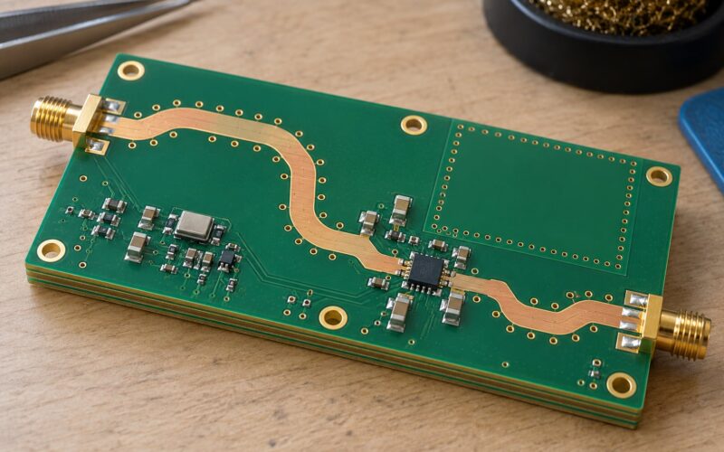
RF PCB Design Guidelines for Beginners: First Layout (2026)
RF PCB design guidelines for beginners, covering stackup, grounding, controlled impedance, RF routing and pre-fab checks that save your first spin ().
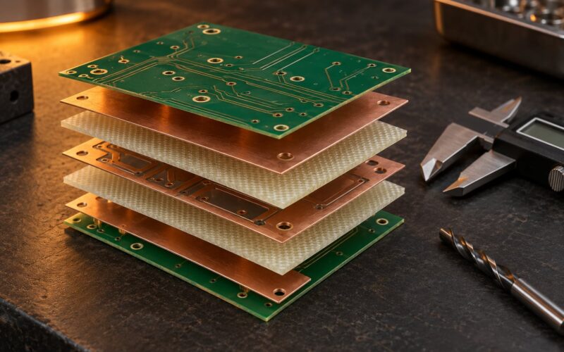
How to Choose PCB Thickness (2026): A Practical Guide
Learn how to choose PCB thickness in for reliability, flex, high-current designs and manufacturing by matching board construction to your requirements.
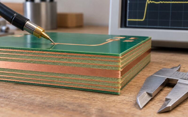
Controlled Impedance PCB Design Guide: Practical Steps (2026)
Controlled impedance PCB design guide: stackup choice, trace and gap calculations, via and layer-transition rules, fab documentation and TDR verification for…
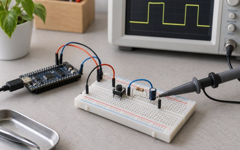
How to Debounce a Switch in Hardware and Software (2026) Guide
Learn how to debounce a switch in hardware and software in using RC filters, Schmitt triggers and millis() timing, with real component…
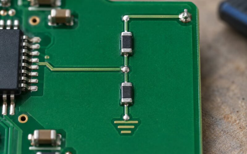
Pull up vs pull down resistors explained in 2026
Pull up vs pull down resistors explained for : how each sets a default logic level, what current it draws, and which…
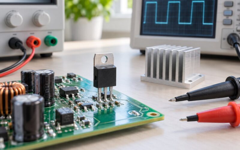
How to Choose a MOSFET for Switching Loads (2026)
Learn how to choose a MOSFET for switching loads by matching voltage, current, Rds(on), switching speed, thermal performance and gate drive. Updated…

How to Read Capacitor Codes and Markings: Simple Guide 2026
Learn how to read capacitor codes and markings in - EIA 3-digit codes, tolerance, voltage, temperature and common SMD formats, with worked…
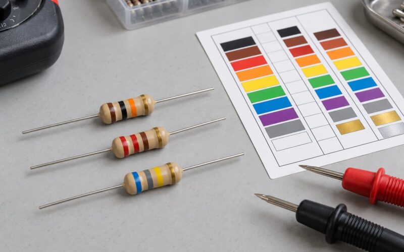
How to Read Resistor Color Codes: A Simple 4-Band Guide 2026
Learn how to read resistor color codes in , calculate resistance, and handle tolerances with clear examples, band patterns, and a practical…
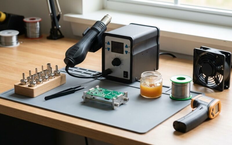
How to Use a Hot Air Rework Station for PCB Repair Safely 2026
Learn how to use a hot air rework station for PCB repair in : nozzle choice, temperature and airflow settings, component removal…
The process stack
Browse by topic
Every guide is filed under the part of the flow it belongs to, from design through fab to assembly and test.
Asked at the design review
Questions this site answers
- What actually happens during a single lithography step?
- Why can a design that passes timing still fail in silicon?
- When does advanced packaging beat moving to a smaller node?
- Which process choices drive the cost of a wafer the most?
What this site is for
A reference for how chips get made
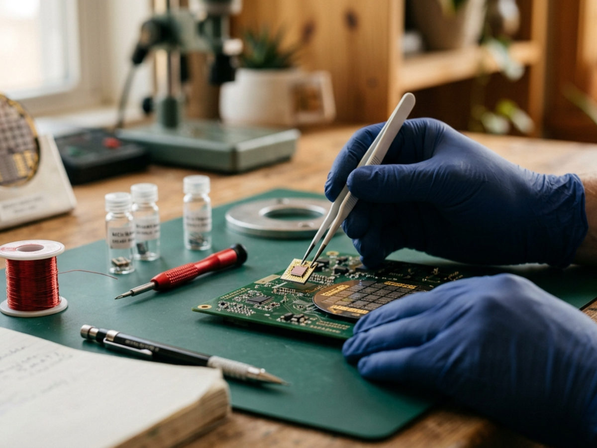
Chartered Semi explains how a chip goes from design intent and mask data through lithography, etch and deposition to assembly, packaging and test, one step at a time and without the marketing layer.
It is written for fabless engineers, EDA and IP users, students reading their way into the industry, and anyone who needs the process described in terms they can use.