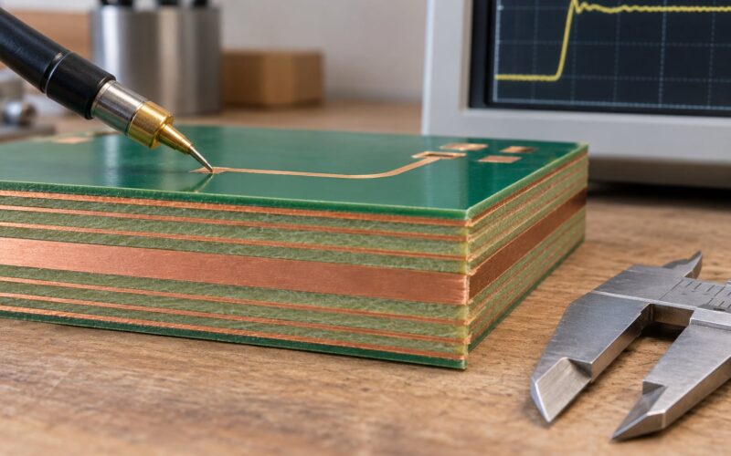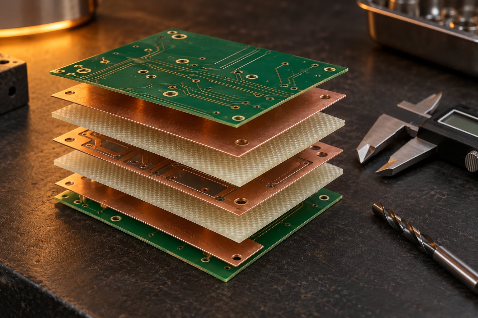
If you are figuring out how to choose PCB thickness for a new board, start at 1.6 mm (about 62 mil) and only move away from it when a mechanical, flex, thermal or enclosure constraint forces your hand. Thickness is not a free parameter you dial in at the end. It is the sum of core, prepreg, copper foil and plating, and it changes drill limits, connector fit, warpage behaviour and how well the board survives handling. In 2026, most designers still land on 1.6 mm because nothing in the design argues otherwise.
This guide works through the decision the way an engineer would: collect the inputs, walk the constraints in order, and confirm the finished thickness with the fabricator before releasing the stack-up.
Table of Contents
- What You Need Before You Choose PCB Thickness
- Standard PCB thickness chart
- How to Choose PCB Thickness: Step by Step
- Start With the Standard or the Application
- Check Mechanical Strength and Connector Loads
- How to Choose PCB Thickness for Flex and Bend Requirements
- Consider Electrical and Thermal Requirements
- Confirm Manufacturing and Assembly Limits
- Common Mistakes
- Frequently Asked Questions
- What is the standard thickness of a 4-layer PCB?
- Why are PCBs 1.6 mm thick?
- What is the recommended thickness for a PCB?
- What is the minimum drill size for a 2.4 mm thick PCB?
- Does PCB thickness affect signal integrity?
- Can I specify a custom PCB thickness?
- Conclusion
What You Need Before You Choose PCB Thickness
You cannot pick a thickness from a datasheet alone. You need the physical and electrical facts of the design first, and you need the fabricator’s process limits, because a thickness nobody can laminate is not an option. Here is the input list I work from before I touch a stack-up.
- Board outline and size. Flexural rigidity scales with the cube of thickness and inversely with the square of span, so a 40 mm module and a 200 mm backplane are not the same problem at 1.6 mm.
- Layer count and copper weight. 1 oz copper is about 35 micrometres of foil; 2 oz is about 70. Both add directly to the finished height and both change how the board behaves mechanically.
- Current per rail and where it flows. Thick copper, wide traces and sometimes a metal core solve heat rise. Thickness alone rarely does.
- Impedance targets and the speed of the signals. What you need is per-layer dielectric height and a defined material (Dk), not a total board height.
- Flex or static. A dynamic bend on a wearable strap and a fixed mounting in a chassis are entirely different constructions.
- Connector, standoff and mounting hardware. Card-edge fingers, press-fit connectors, clips, brackets and spacers are all dimensioned for specific board thicknesses.
- The enclosure. Slot widths, standoffs, bosses and panel cut-outs set hard upper and lower limits.
- Environment and quality class. Vibration, drop, humidity, temperature range, and whether you are building to IPC-6012 Class 2, Class 3, or a defence or aerospace flow such as MIL-PRF-31032.
- Fabricator capability. Their core and prepreg inventory, lamination press thickness limits, tolerance class and drill tooling. Ask early; it changes the answer.
Standard PCB thickness chart
These are the thicknesses fabricators hold as standard. Anything else is a custom build-up, which usually means a different tooling and laminate recipe.
| Thickness (mm) | Mil / thou | Inches | Typical layer count | Typical use |
|---|---|---|---|---|
| 0.4 | 16 | 0.016 | 1-2 | Thin cards, wearables, ultra-thin modules |
| 0.6 | 24 | 0.024 | 1-2 | Compact modules, slim consumer devices |
| 0.8 | 31 | 0.031 | 2-4 | Phones, tablets, small sensor boards, dynamic flex |
| 1.0 | 39 | 0.039 | 2-4 | Small consumer boards, cost-reduced builds |
| 1.2 | 47 | 0.047 | 2-4 | Balanced choice where 1.6 mm will not fit the envelope |
| 1.6 | 62-63 | 0.063 | 1-8+ | The default: industrial control, consumer, most prototypes |
| 2.0 | 79 | 0.079 | 2-6 | Rigid industrial and power boards with heavier parts |
| 2.4 | 94 | 0.094 | 2-8 | Power conversion, backplanes, heavy transformers and relays |
| 3.2 | 126 | 0.126 | 4-12 | Server backplanes, chassis-mount cards, structural applications |
Why does 1.6 mm keep winning? Because tooling grew up around it. Component leads, connector tails, lead-forming dies, panel rails and assembly fixtures were all dimensioned for a board about 62 mils thick. Sticking to 1.6 mm means your parts drop in, the fixture fits and the quote lands on a laminate the factory has pressed a thousand times.
One clarification before you go further, because people conflate them constantly. Board thickness, copper weight and trace width are three separate decisions. Copper weight is how much foil is plated; trace width is a layout choice; finished thickness is the whole build-up. You can have a 1.6 mm board with 1 oz copper carrying 2 A in wide traces, or a 2.4 mm board with 2 oz copper carrying the same current in a narrower space. The thickness tells you rigidity and drill limits. The copper tells you current capacity. The width tells you the current density.
How to Choose PCB Thickness: Step by Step
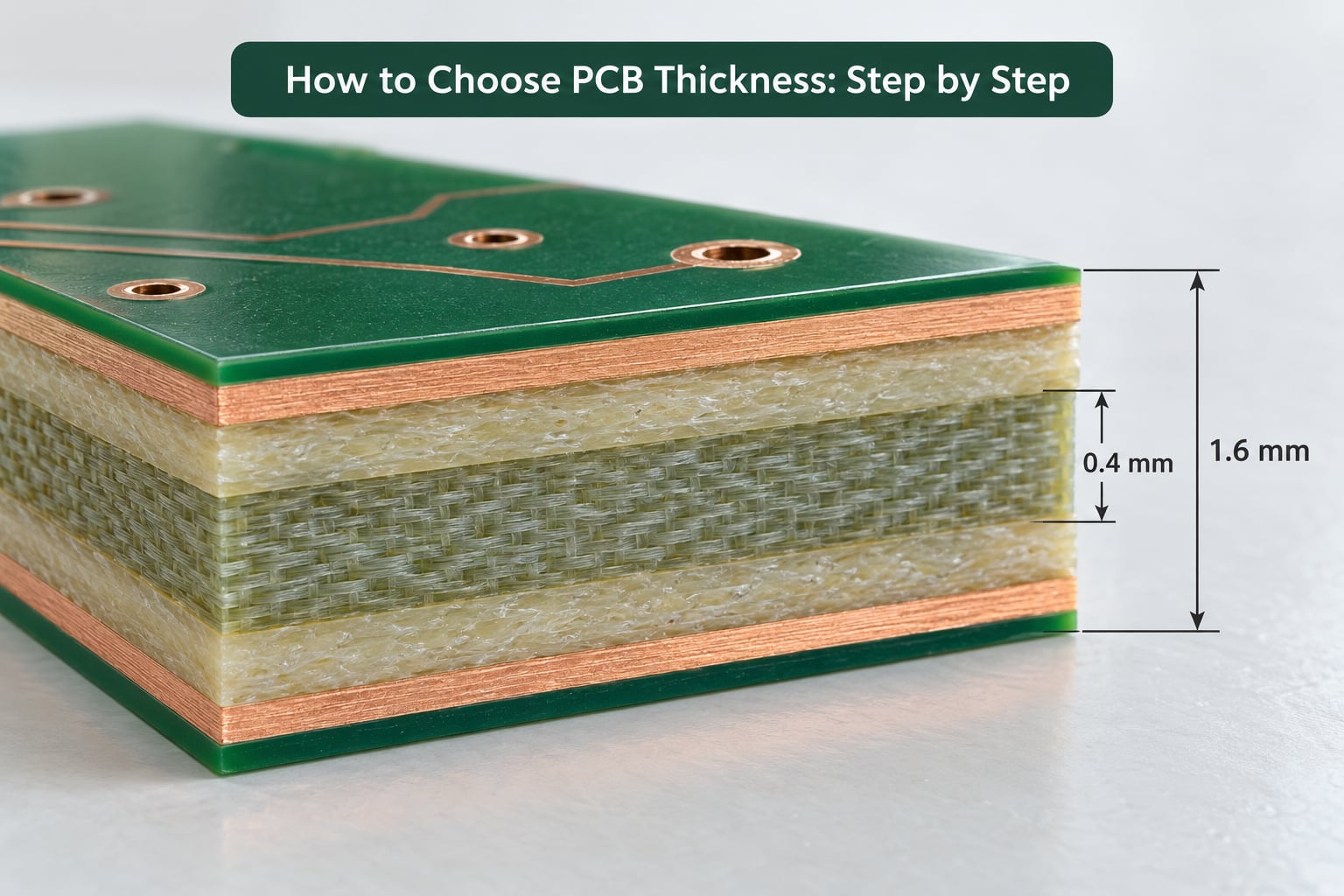
The sequence matters because each step eliminates options for the next. Work top to bottom and you will land on a thickness you can defend on the fabrication drawing.
Start With the Standard or the Application
Pick the nearest standard thickness to your requirement, then check the fabricator can build it. Non-standard builds are not forbidden, but they change tooling, laminate availability and lead time, and the extra cost rarely shows as a separate line on the quote. Most engineers I talk to default to 1.6 mm and only deviate when an enclosure, a mounting feature or a mechanical load forces it.
| Application | Environment | Current on board | Start here |
|---|---|---|---|
| Prototype, MCU board | Bench, indoor | Under 2 A | 1.6 mm, 1 oz |
| Consumer device, phone or wearable | Pocket, hand-held | Under 1 A | 0.8 mm, 1 oz |
| Industrial controller | Vibration, 0-70C | 2-10 A | 1.6 mm, 2 oz on power nets |
| Automotive ECU | Vibration, shock, -40 to 125C | 5-20 A | 1.6-2.0 mm, 2-3 oz, IPC-6012 Class 3 |
| Mains power supply | High ambient, insulation | Over 20 A | 2.4 mm plus, heavy copper or metal core |
| Server or telecom backplane | Slot vibration, card insertion | Varies by rail | 2.4-3.2 mm, 2 oz |
| Dynamic flex in a wearable | Repeated bending | Low | 0.15-0.3 mm flex construction |
| Rigid-flex assembly | Static flex zones plus vibration | Low to mid | Rigid sections at 0.8-1.0 mm, flex sections thinner |
Treat that table as a starting point, not a specification. Your product’s environment decides more than the product category does.
Check Mechanical Strength and Connector Loads
This is where most boards get specified wrongly. Designers look at component weight and total mass, but the failures come from spans, torque and insertion forces rather than static load. A 1.6 mm board with two 200 g transformers mounted near the edge will flex under cable pull even though the total mass seems acceptable. Rigidity comes from three things you can change: material thickness, copper weight on the outer layers, and mechanical reinforcement such as bonded stiffeners or a heavier chassis attachment.
Check these before you settle on a number:
- Unsupported spans. Long distances between mounting holes behave like beams. Flexural stiffness scales with thickness cubed, so going from 1.6 mm to 2.0 mm adds roughly 90 percent more stiffness, while 1.6 mm to 1.2 mm removes about a third of it.
- Mounting-hole spacing. Holes close together do nothing for rigidity. Spread them toward the corners of the heavy regions.
- Cable torque and insertion force. Backplane cards, edge connectors and panel-mount coax all push or twist at the board edge. That is where solder joints crack first, usually a few millimetres out from the connector.
- Vibration and shock. As a working rule, keep the first resonance of the board at least ten times the excitation frequency so vibration response stays in the stiff, low-response region.
- Footprint clearances. Two rules get quoted constantly here. The 3W rule says keep a trace’s width between itself and its neighbour at least three times, which limits capacitive coupling. The 3H rule says leave at least three times the component body height above the board for soldering and cleaning access. Neither rule sets thickness, but both push you toward specific component choices that affect your thickness budget.
If a connector or standoff is dimensioned for a specific thickness, that is a hard constraint, not a preference. Work backwards from it.
How to Choose PCB Thickness for Flex and Bend Requirements
For any circuit that bends, thickness is governed by bend radius, and bend radius is governed by the construction. A static flex that is assembled once and never moves again tolerates a much tighter radius than a dynamic flex that flexes thousands of times. Common industry practice puts the static minimum bend radius at roughly twice the finished thickness and the dynamic radius at about ten times the finished thickness for a two-layer flex circuit, rising further as layer count increases.
Two details decide whether a bend survives. First, the neutral axis: copper on one side only pulls the neutral plane toward itself, which is why flex circuits often use balanced copper on both faces. Second, copper orientation: copper running parallel to the bend axis stretches and cracks under flexing, so in a dynamic bend zone traces should run across the bend, not along it. Flexible, semi-rigid and rigid-flex boards each trade cost against bend life here, and the practical outcome is that dynamic flex uses very thin cores and copper while a static flex zone can carry a thicker core.
Consider Electrical and Thermal Requirements
Finished board thickness does not set characteristic impedance. What sets it is the dielectric height between a trace and its reference plane, the trace width, and the material’s dielectric constant. A 1.6 mm four-layer board with 0.1 mm prepreg needs a much narrower trace for 50 ohms than a 1.6 mm board with 0.3 mm prepreg. Anyone who specifies 1.6 mm expecting an impedance target will miss, and they will miss again when thickness tolerance and dielectric tolerance run in opposite directions.
What thickness does influence electrically is via geometry. A thicker board gives you longer barrels, so more via inductance and more interlayer capacitance, which matters on fast edges and on RF work. Conversely, a thicker board spreads heat better and tolerates the barrel lengths a high-layer-count stack needs. Work the numbers rather than the intuition: IPC-2152 gives temperature-rise estimates for a given copper weight, trace width and allowable rise, and 2 oz copper on the same width and current runs roughly 20 percent cooler than 1 oz.
For genuine power work, copper weight usually matters more than board thickness. Thick copper, wide or paralleled traces, thermal vias under a device and, where the mechanics allow, an aluminium or copper core will do what an extra 0.8 mm of FR-4 cannot.
Confirm Manufacturing and Assembly Limits
Finished thickness is arithmetic, and it is worth doing before you send anything to a fabricator. Take a four-layer board: 1.0 mm glass core plus two layers of 106 prepreg at about 0.2 mm each gives 1.4 mm of dielectric. Four layers of 1 oz copper add 0.14 mm, so the raw build is 1.54 mm. Plating, surface finish and solder mask take it to a finished thickness near the 1.6 mm nominal. Now double the copper to 2 oz and the same nominal 1.6 mm needs a thinner core, because the fabricator has to remove 0.07 mm to land back on target. That single change is why a 2 oz board and a 1 oz board are not interchangeable even at the same stated thickness.
Drill aspect ratio is the next limit. Fabricators generally hold holes to a maximum aspect ratio of about 10:1, meaning hole diameter should be at least one tenth of the finished board thickness. A 2.4 mm board therefore has a practical minimum drill of roughly 0.24 mm. Ask for that number in writing before you place 0.15 mm microvias, and expect to move to laser-drilled microvias in a separate build step if your design depends on them.
Tolerance is where this bites hardest. A typical finished thickness tolerance is plus or minus 10 percent, while impedance targets are often held to plus or minus 5 or 10 percent across a controlled impedance stack-up. A board that lands at 1.44 mm when you asked for 1.6 mm may still meet its impedance spec, because the dielectric heights inside the stack were controlled separately. Confirm that your fabricator controls dielectric height rather than relying on the overall thickness to land where you want it.
Finally, check the mechanics of manufacturing and assembly. Panelisation rails, tooling holes, castellations and edge connectors all assume a thickness. Thicker boards need different drill and routing consumables, and they take more force to shear. Assembly fixtures, depanelisation and any press-fit or card-edge hardware must match the finished thickness, not the nominal one. Then re-check the enclosure with the tolerance band in hand: if the slot is 1.6 mm and your board can be 1.75 mm, you have a manufacturing stop before you have a product.
Common Mistakes
Most thickness problems trace back to one of five habits. Fixing them early costs nothing; fixing them after tooling does.
Choosing thickness without doing the stack-up arithmetic. Treat 1.6 mm as a target outcome rather than an input. Add core, prepreg, copper and finish yourself, then let the fabricator confirm it, because they may substitute a core that changes the dielectric height and your impedance.
Assuming a thicker board improves electrical performance. It does not set impedance, it makes fine-pitch etching and drilling harder, and it lengthens every via barrel. Specify dielectric height for signal integrity and copper weight for current, then pick thickness for mechanics.
Ignoring bend radius. A rigid-flex design that looks fine flat can crack at the first fold if the dynamic radius was set for a static assembly. Decide early whether a zone bends once or ten thousand times.
Discovering enclosure clearance after tooling. Give the mechanical engineer the tolerance band, not the nominal number, and agree the board stack-up before the enclosure is machined.
Approving a stack-up without fabricator review. They know which cores and prepregs they actually hold and which builds their press and drill can hit consistently. A short review before fabrication is far cheaper than a rejected panel.
One last tip: put the finished thickness, the tolerance, the stack-up, the copper weight and the mechanical requirements in writing on the fabrication drawing. When a board arrives off-spec, that drawing is what turns a dispute into a conversation.
Frequently Asked Questions
What is the standard thickness of a 4-layer PCB?
A four-layer board is normally built at 1.6 mm, which is the same default used for one- and two-layer boards. Anything thinner tightens the dielectric spacing and makes routing harder; anything thicker costs more and changes the tooling. If you need a custom value such as 1.0 mm or 2.0 mm, confirm it against the fabricator’s available cores before you commit.
Why are PCBs 1.6 mm thick?
1.6 mm, roughly 62 mils, became the default because component leads, lead-forming tooling, connector tails and assembly fixtures were all dimensioned for a board that thick. Fabricators hold cores and press recipes for it, so it laminates consistently and quotes quickly. Deviating from 1.6 mm is a real engineering decision, not a preference.
What is the recommended thickness for a PCB?
For most products, 1.6 mm is the recommended starting point. Use 0.8 mm for slim consumer devices and dynamic flex, 2.0 to 2.4 mm for power conversion, heavy transformers and industrial boards, and 3.2 mm for backplanes and slot cards. Let connector hardware, enclosure slots and mechanical loads overrule these defaults before you finalise the stack-up.
What is the minimum drill size for a 2.4 mm thick PCB?
Most fabricators hold a maximum drill aspect ratio near 10:1, so a 2.4 mm board has a practical minimum finished hole of about 0.24 mm. Thinner mechanical drills may be possible but break out or wander, and smaller holes require laser-drilled microvias built in a separate process step. Ask your fabricator for its aspect-ratio limit in writing before placing small vias.
Does PCB thickness affect signal integrity?
Only indirectly. Characteristic impedance is set by dielectric height, trace width and the material’s dielectric constant, not by total board thickness. Thickness still changes via inductance and interlayer capacitance, and it interacts with thickness tolerance, so specify the stack-up and dielectric heights rather than relying on a nominal board height to hit your impedance target.
Can I specify a custom PCB thickness?
Yes, most fabricators build custom thicknesses such as 1.0 mm, 2.0 mm or 2.5 mm using different core and prepreg combinations. The trade-offs are a different tooling and laminate recipe, potentially longer lead time, and a tolerance that is usually wider than the standard band. Send the fabricator your target finished thickness and tolerance early, and ask for the stack-up they intend to use.
Conclusion
Choosing PCB thickness comes down to five inputs in order: the application and its environment, the mechanical loads from components, connectors, cables and vibration, the flex or bend requirement, the electrical and thermal targets, and finally the fabricator’s process limits. Start at 1.6 mm and move only when one of those inputs moves with you. Send the fabricator your target thickness, tolerance and stack-up before release, and get their confirmation in writing.