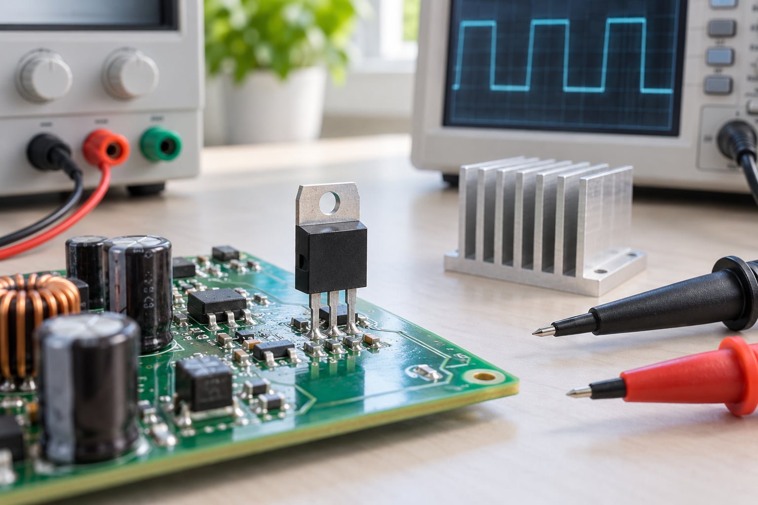
Choosing a MOSFET for switching loads comes down to matching five numbers to your circuit: the drain-source voltage rating, the drain current rating, the on-resistance Rds(on), the gate drive voltage you actually have available, and the package’s ability to get rid of the heat. Get those right and the part switches cleanly; get one wrong and it runs hot, never fully turns on, or dies on the first transient.
Most beginner mistakes come from reading a datasheet’s headline numbers as design limits. The continuous drain current rating is a thermal claim, not a promise. The threshold voltage is not the gate voltage you should use. Neither number is a safe operating limit.
The process below follows a fixed order because each step removes candidates. Work through it once and the shortlist is usually two or three parts wide, which makes the final comparison easy.
Table of Contents
- What You Need
- Step-by-Step: How to Choose a MOSFET for Switching Loads
- 1. Define the load and switching conditions
- 2. Check voltage and current ratings with margin
- 3. Calculate conduction and switching losses
- 4. Select the right gate-drive method
- 5. Verify thermal performance and protection
- 6. Compare candidates and validate the choice
- Common Mistakes
- Frequently Asked Questions
- Do I need a low-RDS(on) MOSFET for a switching load?
- Is the MOSFET maximum current rating safe to use continuously?
- What gate voltage should I use for a power MOSFET?
- How do I calculate MOSFET switching loss?
- Can I use a logic-level MOSFET with a 5 V microcontroller?
- What MOSFET do I choose for an inductive or motor load?
- Conclusion
What You Need
Gather these before opening any datasheet. Without them, every comparison you make is a guess.
- Load voltage: the highest voltage the drain will ever see, including supply tolerance, transient overshoot and any back-EMF.
- Load current: steady-state current, plus startup inrush for motors, capacitors and filaments.
- Load type: resistive, inductive (solenoid, relay coil, motor winding), or capacitive/inrush-limited.
- Switching frequency and duty cycle: how often the device transitions and what fraction of the time it conducts.
- Ambient temperature and cooling: the air temperature at the board and whether a heat sink is possible.
- Gate drive details: the controller output voltage, its source and sink current capability, and whether a driver IC is available.
- Topology: low-side switching to ground, or high-side switching to a positive rail.
This table sets out which parameters deserve attention for each load character. Read the row that matches your load first.
| Load character | Parameters that decide the part | Protection you cannot skip |
|---|---|---|
| Resistive (heater, lamp bank) | Vds headroom, continuous current rating, conduction loss at high duty cycle | No flyback diode needed; current limiting on cold-start inrush |
| Inductive (solenoid, relay coil, motor winding) | Vds headroom for back-EMF, avalanche rating, Rds(on) | Flyback or freewheel diode sized to the load current |
| Motor with startup inrush | Pulse current capability, SOA for the stalled condition | Current limiting or soft start; diode sized for stall current |
| LED bank or capacitive load | Continuous current rating, output capacitance, switching loss at frequency | Bulk capacitance at the drain; gate resistor for dv/dt control |
One more thing to have on hand: a parametric search at a distributor. Browsing filtered by Vds, current, package and Rds(on) is faster than guessing part numbers, and it surfaces the second sources you want for production.
Step-by-Step: How to Choose a MOSFET for Switching Loads
1. Define the load and switching conditions
Write down the worst case, not the typical case. For a 12 V rail that can sit at 14.4 V, the drain sees 14.4 V, and the value you design against is that number rather than the label on the battery.
For current, record two figures: the current the load draws once it has settled, and the peak it draws during startup. A DC motor can draw several times its running current while the shaft is stationary, and a solenoid draws its full coil current every time it energises.
Then settle the polarity question. Does the load sit between the supply and the drain, or between the drain and ground? And does the circuit ever see reverse voltage across the drain-source terminals when the device is off? A part with a body diode will pass current one way even when the gate is held low, which matters for reverse-polarity protection and for loads that feed energy back.
2. Check voltage and current ratings with margin
Compare your worst-case voltage against the drain-source breakdown voltage, and your worst-case current against the continuous drain current rating, keeping margin on both. Practitioners on the All About Circuits forum settled on multiplying the required current by roughly four before picking a rating, and that consensus still holds up: going one size larger costs almost nothing, while going too small costs the board.
Understand what each rating actually means before you rely on it:
- Continuous drain current is limited by how much heat the package can shed. It assumes a specific case temperature and a specific board. On a different PCB with no copper pour, the real limit is lower.
- Pulsed drain current is a short-duration capability tied to a stated pulse width. It is not a continuous rating and cannot be used for a steady load.
- Drain-source breakdown voltage is where the device fails catastrophically. Add 40 to 50 percent headroom over your worst-case rail so that inductive overshoot and supply spikes do not push you into avalanche.
These numbers answer different questions, so treating them as interchangeable is the classic selection error. A part with a large continuous current rating can still be destroyed by a voltage spike it was never meant to block.
Worked example: a 24 V actuator drawing 2 A steady and 6 A inrush. A part rated 60 V / 4 A continuous survives the voltage margin easily, and 4 A against a 2 A steady load is the 2x minimum. Against the 6 A inrush you need to check the pulse rating rather than assume the continuous figure covers it.
3. Calculate conduction and switching losses
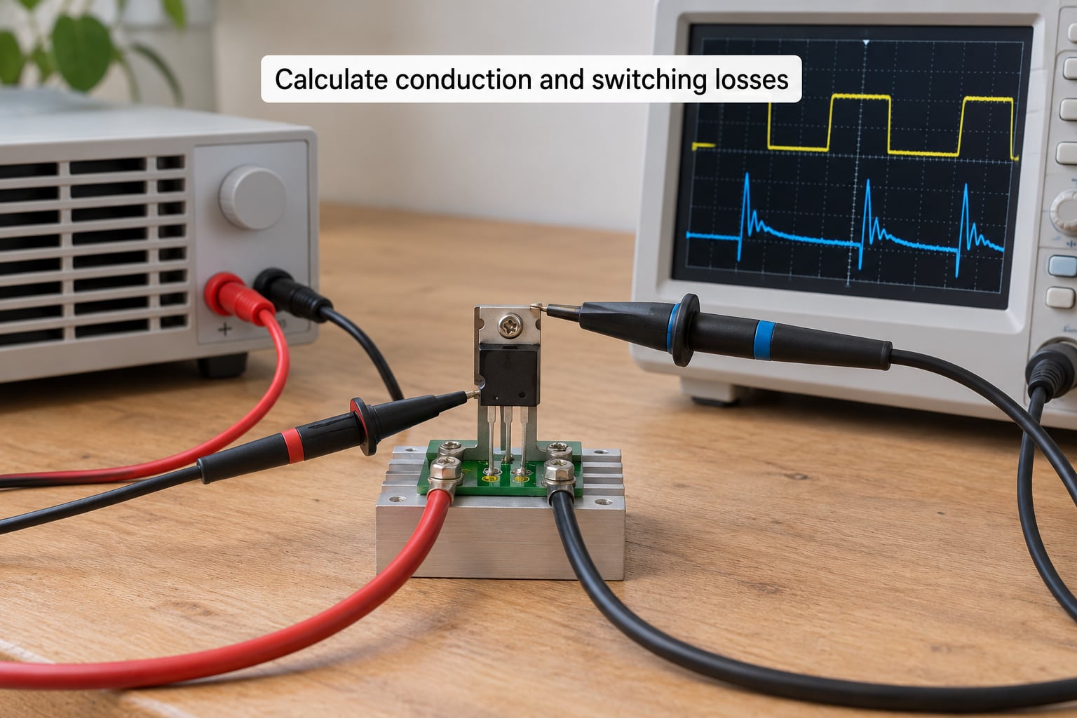
The on-state loss is one line of arithmetic: P = I² x Rds(on). That result is watts of heat, and the package has to dissipate it.
Two details catch people out here. First, Rds(on) is measured at a specified gate voltage and a specified temperature, and it rises substantially as the part heats up. Use the figure for your actual gate drive, not the headline value at 10 V, and use the hot value rather than the 25 °C figure if your device will run warm.
Run the numbers on the three examples. At 3 A through a 50 milliohm part at 25 °C, loss is 9 x 0.05 = 0.45 W. If the same part is specified at 100 milliohm at your 4.5 V gate drive, that becomes 0.9 W. At the same current, the second part needs roughly twice the copper area or a heat sink.
Switching loss depends on how often you switch, not how long you conduct. It scales with the gate charge Qg, the drain current, and the blocking voltage, and it rises with frequency and falls with duty cycle. For a load switched a few times per second, conduction loss dominates and Rds(on) is the only number that matters. For PWM at tens of kilohertz, switching loss and output capacitance Coss take a real share of the budget, and a lower-Qg part can beat a lower-Rds(on) part.
That is why selecting on Rds(on) alone is a mistake. It is the right criterion for a slow, mostly-on switch and the wrong one for a fast PWM chopper.
4. Select the right gate-drive method
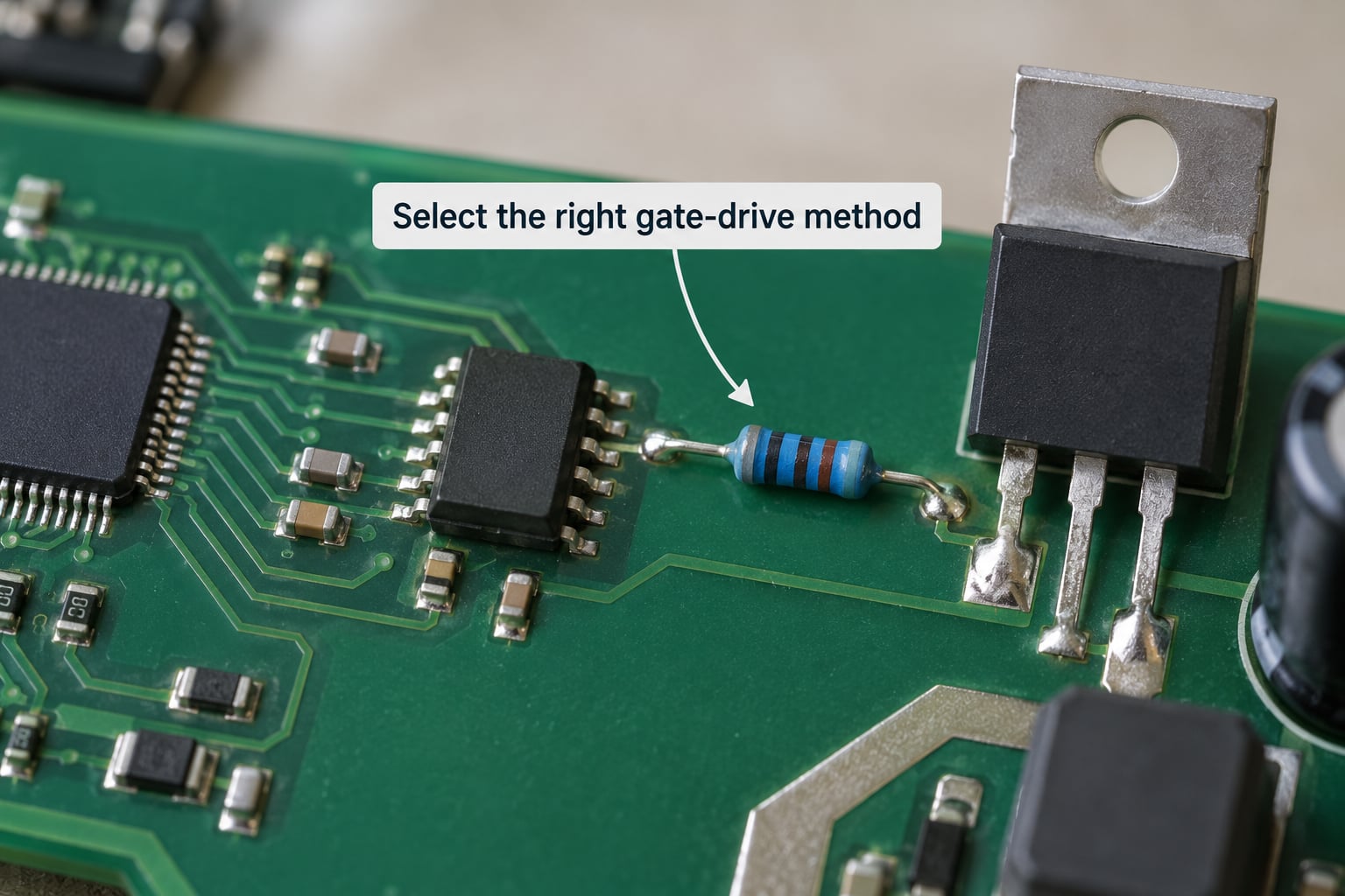
The gate voltage decides whether the device is on or merely conducting. Check two different numbers: Vgs(th), the threshold at which current begins to flow, and the recommended gate voltage from the datasheet’s electrical characteristics, which is where the manufacturer specifies the Rds(on) you should expect.
A standard-level part typically wants around 10 to 12 V at the gate. A logic-level part is specified to be fully enhanced at 4.5 V, and many modern devices are specified at 2.5 V or 3.3 V as well. Driving a standard-level part from a 5 V microcontroller leaves it partially on: it conducts, it runs hot, and the thermal runaway pattern is well documented.
So yes, you can drive a logic-level MOSFET directly from a 3.3 V or 5 V microcontroller, but only if the datasheet lists an Rds(on) value at that exact gate voltage. If the datasheet shows Rds(on) only at 10 V, treat the part as standard-level regardless of what the marketing page says.
Gate drive also has a speed dimension. The driver must source and sink the peak current required to charge and discharge the gate capacitance, and that peak current is roughly (drive voltage minus threshold) divided by the internal gate resistance. A microcontroller pin can supply a few milliamps, which is why large parts or fast edges need an external driver.
Add two resistors and both are standard practice. A pull-down of a few kilohms from gate to source holds the device off when the controller resets or the pin floats. A series gate resistor of a few ohms slows the edge, damps ringing on the gate trace and limits the rate at which drain current changes. Both values are starting points that you trim by watching the gate on a scope.
5. Verify thermal performance and protection
Work from the loss you calculated in step 3 and the thermal resistance of the package. The junction temperature estimate follows from total dissipated power multiplied by the effective thermal resistance from junction to ambient, added to the ambient temperature. That result has to land well below the maximum junction rating with margin, not just touch it.
Package choice follows from that calculation and from the assembly. Through-hole parts in TO-220 carry far more heat than surface-mount parts with a small exposed pad, and the thermal resistance figures in datasheets assume a specific amount of copper. Move a small package from a generous pour to a thin trace and the junction temperature can rise by tens of degrees.
| Package | Where it fits | Thermal note |
|---|---|---|
| TO-220 | Heavier loads, through-hole builds, anything needing a heat sink | Needs real copper or a heat sink above a watt or so |
| DPAK / TO-263 | Surface-mount designs in the 5 A to 20 A class | Exposed tab ties to the drain; pad size drives the number |
| SOT-23 | Small surface-mount designs, sub-amp switching | Little copper means sub-watt losses only |
| TO-92 | Breadboard and through-hole prototypes | Practitioners put fine on/off switching up to roughly 500 mA here |
Protection is where the drain-source layout and the load type meet. For any inductive load, place a flyback diode across the load, cathode to the positive side, as close to the load as you can manage. Size it for at least the load’s steady current, with a reverse voltage rating above your supply. The community reference part quoted in the All About Circuits thread, an IRLD014PBF rated 60 V with 0.2 ohm on-resistance and a 1 A rating, was chosen on exactly this kind of per-partner arithmetic rather than on a headline current figure.
Other protections worth checking: the avalanche energy rating if the load can dump energy back with no diode, the safe operating area if the device will ever be partially on rather than fully on or fully off, a current shunt if you need to sense the load, and a bulk capacitor at the drain on long or fast wiring runs.
6. Compare candidates and validate the choice
Now put the surviving parts side by side on the same set of columns: Vds rating, continuous and pulsed current, Rds(on) at your gate voltage, recommended gate drive, total gate charge, package, thermal resistance, second source available.
Re-open each datasheet and confirm the test conditions behind every number you are relying on. Rds(on) quoted at 10 V tells you nothing about a 3.3 V drive. Current ratings assume a case temperature you may not have. Loss figures quoted at 25 °C are optimistic for a device inside a sealed enclosure.
Before committing, model the switching behaviour if you have the tools, build the circuit on a prototype board, and put a scope on the gate, the drain and the source. Check that the gate voltage reaches its full commanded value, that the drain edge is clean, that no overshoot exceeds your headroom, and that the case temperature settles at the expected value under worst-case load rather than a few minutes of bench testing.
The bench check is where mistakes surface. A ringing gate trace that turns the device on for a few nanoseconds when it should be off, or a diode that is too slow for the inductive energy, will show up on the scope long before they show up as a failed board in the field.
Common Mistakes
These are the selection errors that come up repeatedly, each with the correction that fixes it.
| Mistake | What it causes | Fix |
|---|---|---|
| Designing to the maximum current rating | Overstressed device that runs at the datasheet limit with no margin | Derate by roughly 4x on continuous current, and confirm the SOA for transients |
| Ignoring thermal limits | Thermal runaway, then failure | Compute I² x Rds(on) and check junction temperature against the package thermal resistance |
| Confusing Vgs(th) with full enhancement | Device sits in the linear region and dissipates far more than expected | Use the datasheet’s recommended gate voltage, not the threshold value |
| Neglecting transients and inrush | Avalanche breakdown or SOA violation at startup | Check pulse current rating, SOA curve and startup behaviour explicitly |
| Selecting on Rds(on) alone | Bad choice for high-frequency PWM, where switching loss dominates | Weigh gate charge and output capacitance alongside on-resistance |
| Overlooking reverse current and the body diode | Current flows in the off state, defeating the switch | Plan for the body diode direction or add a blocking device in series |
| No flyback diode on an inductive load | The stored energy dumps through the device and destroys it | Fit a freewheel diode across the load, sized to load current |
| No gate pull-down or gate resistor | False turn-on during reset, ringing on the gate trace | A few kilohms gate-to-source, and a few ohms in series at the gate |
Two more that catch experienced builders. Putting the load in the source circuit rather than the drain raises the source voltage as current flows, which creeps toward the gate voltage and can shut the part down partway through operation. And exceeding the gate-source absolute maximum, commonly plus or minus 20 V, is a fast way to destroy the gate oxide, whether it happens from ESD or from a slow ramp on a high-charge part.
If you are new to reading these documents, work through one part end to end rather than comparing ten at once. Once the parameter meanings are familiar, the comparison itself becomes mechanical.
Frequently Asked Questions
Do I need a low-RDS(on) MOSFET for a switching load?
Only when the device spends most of its time on. Rds(on) sets conduction loss through I squared times Rds(on), so for a load switched a few times a second it is the dominant term and worth minimising. For fast PWM, switching loss and output capacitance take a large share, and a lower-gate-charge part can win even with higher on-resistance.
Is the MOSFET maximum current rating safe to use continuously?
Not as a design target. The continuous drain current rating is a thermal limit tied to a stated case temperature and a specific board with a specific amount of copper. Derate it by roughly four times for a design margin, then confirm junction temperature with your own thermal calculation. Pulse ratings are separate and cannot be used for steady load.
What gate voltage should I use for a power MOSFET?
Use the datasheet recommended gate voltage, not the threshold. A standard-level part wants around 10 to 12 V; a logic-level part is specified at 4.5 V and many modern devices at 2.5 or 3.3 V. Whatever you drive, keep it inside the gate-source absolute maximum, commonly plus or minus 20 V, or you risk damaging the gate oxide.
How do I calculate MOSFET switching loss?
Switching loss scales with drain current, blocking voltage, switching frequency and gate charge, so it rises steeply with frequency. Compare candidates by working out their total gate charge and output capacitance at your drive voltage and estimating the overlap time in the transition. For slow on/off switching, conduction loss dominates and this calculation can be skipped.
Can I use a logic-level MOSFET with a 5 V microcontroller?
Yes, provided the datasheet lists an Rds(on) figure at that gate voltage. A 5 V pin can also drive a 3.3 V-rated part, though a part specified only at 10 V will sit partially on and overheat. Keep peak gate current within the pin’s drive capability, add a gate pull-down, and remember the pin’s absolute maximum voltage is far lower than the MOSFET’s.
What MOSFET do I choose for an inductive or motor load?
Pick on voltage headroom, current rating and avalanche behaviour rather than on-resistance alone. Budget for the back-EMF peak above your supply when choosing the drain-source rating, size the drain current rating against the running and stall currents, and fit a flyback diode across the load with a reverse voltage rating above your rail. For motors, check the safe operating area for the stalled condition.
Conclusion
Start with the worst case your load can produce, not the nominal case. Write down the maximum drain voltage, the steady current, the inrush peak, the switching frequency and the gate drive voltage you actually have, then work outward: voltage and current with margin first, then conduction and switching loss, then gate drive, then package and protection. Each of those checks narrows the candidate list.
The first thing to do after that is pull the datasheet for your two or three remaining parts and read the test conditions behind every number. Match them to your real circuit, then verify on the bench with a scope on the gate and drain before the design goes any further.