RF PCB design is the practice of laying out a circuit board so signals above roughly 100 MHz travel predictably. You control the characteristic impedance, keep a continuous ground return path directly beneath every trace, pick a laminate that loses too little signal, and match the whole stackup to the frequency band you are actually working in. Get those four things right and the board mostly works. Skip any of them and no amount of careful schematic work saves you.
Most of the RF PCB design guidelines for beginners floating around the internet are written as an undifferentiated list of rules, which is exactly why they are hard to use. A 2.4 GHz sensor node and a 7 GHz receiver are both “high frequency”, but the material, the stackup, the routing discipline and the verification method differ substantially between them.
So this guide is organised the way a first layout actually happens. You define the requirements, choose a stackup, plan the return paths, place the RF chain, route, add the mechanical and protection details, and then check the work before you spend money on boards. Each step includes the number or the geometry that tells you whether you got it right.
One warning before you start. A prototype board is the right place to make mistakes cheaply, which is the whole point of prototyping, but the failure modes at RF are less forgiving than at DC. On a digital board a slightly wrong trace width is just a slightly different delay. At 2.4 GHz a quarter wavelength on FR-4 is about 31 mm, so features you would consider invisible are large enough to act as antennas, resonators or filters.
Table of Contents
- What You Need
- Step-by-Step RF PCB Design Process
- 1. Define the RF Requirements and Board Constraints
- 2. Choose the Layer Stackup and Impedance Targets
- 3. Plan Grounding, Power, and Isolation
- 4. Place the RF Chain and Connectors
- 5. Route RF Traces and Control Crosstalk
- 6. Add Protection, Test Points, and Manufacturing Details
- 7. Validate the Design Before Fabrication
- Common RF PCB Design Mistakes
- Frequently Asked Questions
- Is FR-4 good enough for RF, or do I need Rogers?
- How many PCB layers do I need for RF?
- Why do I need a ground plane under an RF trace?
- What is the difference between microstrip and stripline?
- How do I verify my RF PCB layout before fabrication?
- How do I choose a trace width for 50 ohm?
- Conclusion
What You Need

Before you open a layout tool, you need four things settled in writing: the requirements, the stackup, the impedance target and the verification path. The rest of this guide assumes you have them. If any one is still open, close it first, because every later decision depends on it.
- A requirements sheet. Operating frequency or band, output power, the impedance you are working with, connector type, antenna type, board outline and enclosure limits, and the manufacturing tolerances you are prepared to accept.
- A stackup you can actually order. Layer count, laminate, copper weight, finished board thickness, and the impedance values the fabricator supports. If the fabricator cannot build the stackup you want, the design is already wrong.
- An impedance target per net class. 50 ohm is the radio default; 75 ohm shows up around video and antenna feeds; differential pairs carry their own target. Every net class needs a width and a reference plane named against it.
- A PCB tool that supports constraints. KiCad is a genuine entry point for RF layout these days; Altium Designer, Cadence OrCAD and Allegro are what most professional teams use. What matters is that the tool lets you assign a stackup, define net classes with impedance values, and run a field solver or a constraint-driven check against them.
- An impedance calculator or field solver. Free online conformal-mapping calculators cover microstrip and stripline well enough for a first board. A field solver inside the layout tool is better, because it accounts for the actual geometry including solder mask and neighbouring traces.
- Measurement gear, at least planned for. A vector network analyser is the real tool. A time-domain reflectometer is a workable substitute for impedance verification. Even on the first prototype, decide now how you will confirm the result, because “it doesn’t transmit” is not a diagnostic.
One more thing worth settling early: who fabricates the board. Forum discussions about first RF boards keep circling the same advice, which is that asking the fabricator for their stackup table, their design-for-manufacturing report and their impedance calculation support is the cheapest error-correction available to you. It is free, and it catches mismatched assumptions before copper is poured.
Step-by-Step RF PCB Design Process
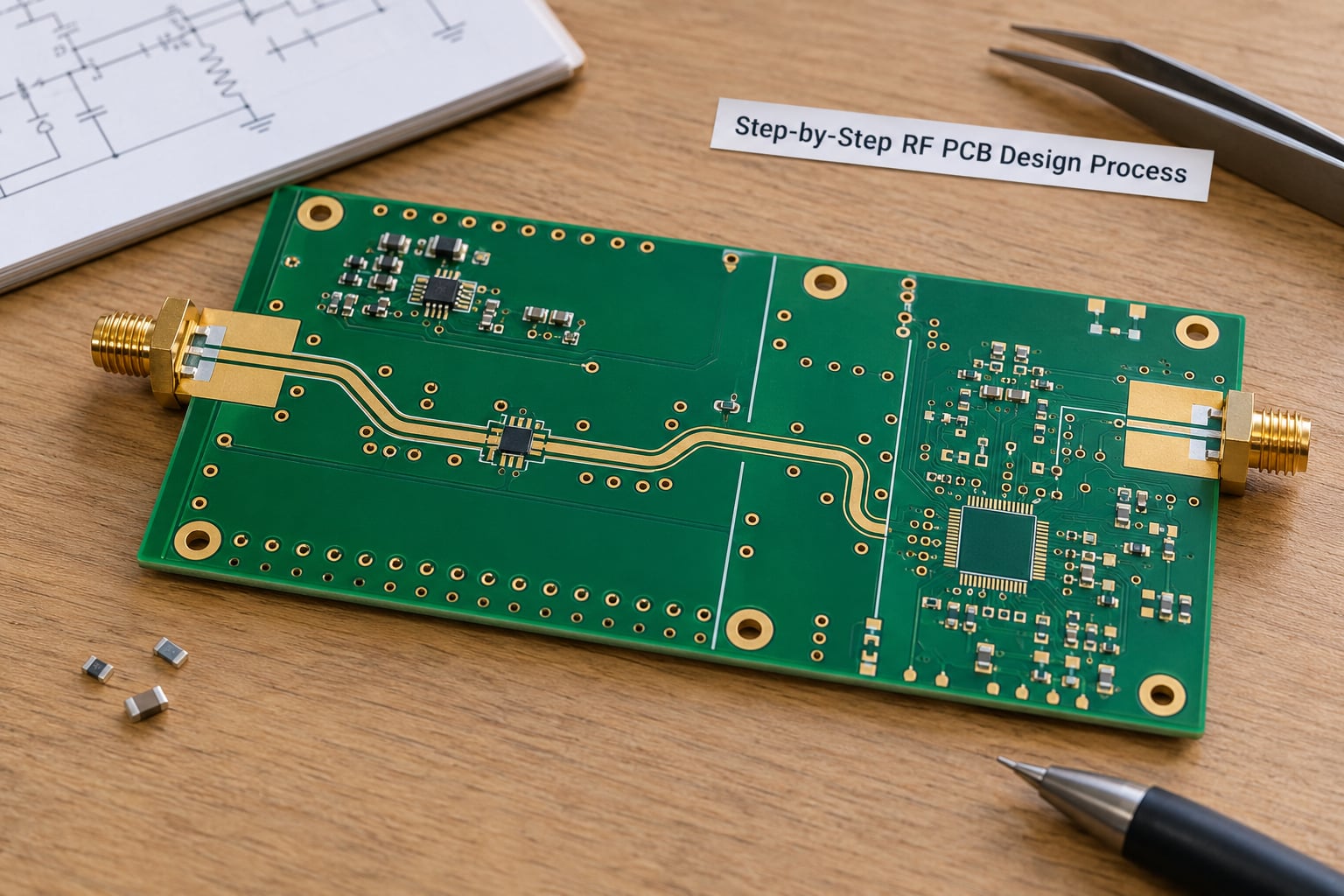
The process below is the order that keeps decisions cheap, and it is the sequence these rf pcb design guidelines for beginners follow end to end. Each step is a gate: if you cannot answer the check at the end of a step, going forward costs you a respin.
1. Define the RF Requirements and Board Constraints
Write down the operating band before you pick a single component. Is it a single frequency or a wideband signal? Does it need to cover 2.4 GHz and 5 GHz in the same board? Wideband changes the calculus because laminate dispersion, which is negligible in narrowband work, starts to matter.
Then record power level, signal type (single-ended, differential, or a modulated waveform with real bandwidth), connector requirements, maximum board size from the enclosure, and the mounting hole positions. Those mechanical constraints usually bind harder than people expect, and moving a mounting hole after the RF layout is placed wrecks the ground and the antenna clearance.
Check: you can state the highest frequency on the board, the impedance of every net class, and the board outline in millimetres without looking anything up.
2. Choose the Layer Stackup and Impedance Targets
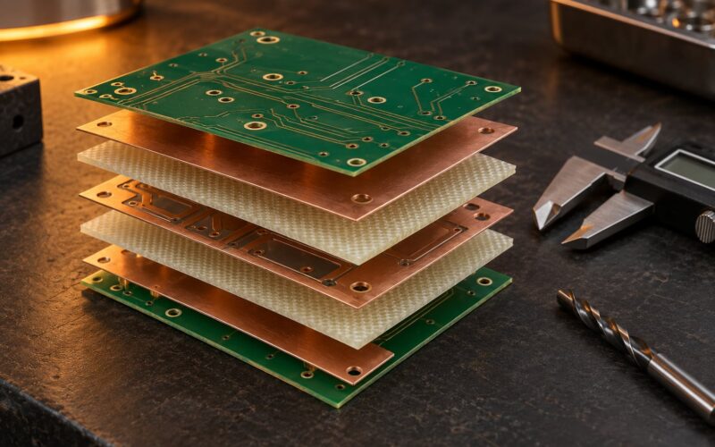
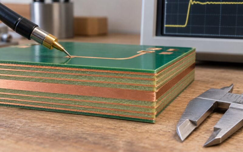
Stackup comes before routing because routing depends on it. One-layer boards cannot do controlled impedance at all. Two-layer boards work, but only in a limited envelope: with the ground plane on the bottom and components on the top, the entire board thickness becomes your substrate height, so a standard 1.6 mm FR-4 board puts a very wide microstrip on a very thick dielectric and the impedance maths gets unforgiving. Keep total thickness modest, around 30 mils or less, for two-layer RF boards and treat any impedance target as approximate.
Four layers is where most first RF designs land: signal on top, ground underneath it, then power and signal below. Eight layers only makes sense on a genuinely mixed-signal board, and even then the point is keeping fast digital layers away from the RF layers rather than adding copper for its own sake. If your board mixes a radio with a processor, a plain-language explanation of the floorplanning problem is in what mixed signal design is.
On material, the honest summary is that FR-4 works well into the low GHz and gets expensive fast above that. It is generally considered usable to about 6 GHz, which covers 2.4 GHz Wi-Fi comfortably. Rogers-class laminates such as RO4003C and RO4350B give a tighter dielectric constant and a much lower loss tangent, and PTFE-based laminates go further still. Watch the dielectric constant: FR-4 inner core and prepreg are not the same value, and a stackup mixing 4.2 with 3.8 will not behave the way a calculator assuming one uniform number predicts.
Check: the fabricator has confirmed the stackup in writing, the impedance tolerance is stated, and you know which layer is the reference plane for each RF net class.
3. Plan Grounding, Power, and Isolation
The return path is the part beginners skip and the part that causes most failures. At high frequency, current does not return along the trace directly beneath it. It returns in the adjacent plane along the shortest path that completes the field, and if the plane is interrupted the return current has to detour around the gap, which lengthens the loop, adds inductance and radiates.
So keep one continuous ground reference under the RF region. The specific anti-pattern worth naming, because it appears in guidance aimed at mixed-signal boards, is splitting the plane into separate digital and analog islands and joining them with a capacitor. A capacitor is a poor high-frequency return path. Use one unbroken plane and control the return current by routing discipline instead. If you want to know what each net class and its return current are doing on paper, design rule checking explained for beginners is a useful primer on turning that intent into constraints.
On power, decouple every pin with its own bypass capacitor placed as close to the pin as the package allows, and give each one a dedicated ground via to the reference plane rather than making it share a via with a neighbour. Above the capacitor’s self-resonance frequency it stops helping and starts behaving like an inductor, which is why the value choice matters as much as the placement. Keep switching regulators, DC-DC converters and high-current paths physically away from sensitive RF nodes, and put a via fence of ground stitching around RF sections that sit next to noisy ones.
Check: every RF trace has an unbroken plane directly beneath it, and no plane split exists anywhere under an RF net.
4. Place the RF Chain and Connectors
Place the whole chain in signal order: antenna, matching network, filter or duplexer, low-noise amplifier or power amplifier, switch, then mixer and baseband. Moving a stage sideways to make the layout prettier costs you a longer trace and a worse return path.
Connectors need more thought than most beginners give them. Decide the orientation before placement, because an SMA that faces the board edge is easy to probe and an SMA that faces inward is a permanent soldering problem. Give the connector’s return pins their own vias into the reference plane rather than letting them share a path with the signal. Keep the connector and its launch region free of copper pour on the top layer where the launch geometry requires it, since an unintended top-layer ground close to a microstrip changes its impedance.
For on-board antennas, respect the keep-out. A chip or printed antenna has a defined keep-out region that must contain no copper, no ground pour and no enclosure metal, including fasteners. If the antenna sits at a board edge, the ground plane usually needs to be pulled back underneath it by the distance the antenna design specifies, and that pullback has to be in the design intent, not improvised during layout.
Check: the chain runs in one direction, connector launches have their own ground vias, and the antenna keep-out area is drawn on a mechanical layer you can see.
5. Route RF Traces and Control Crosstalk
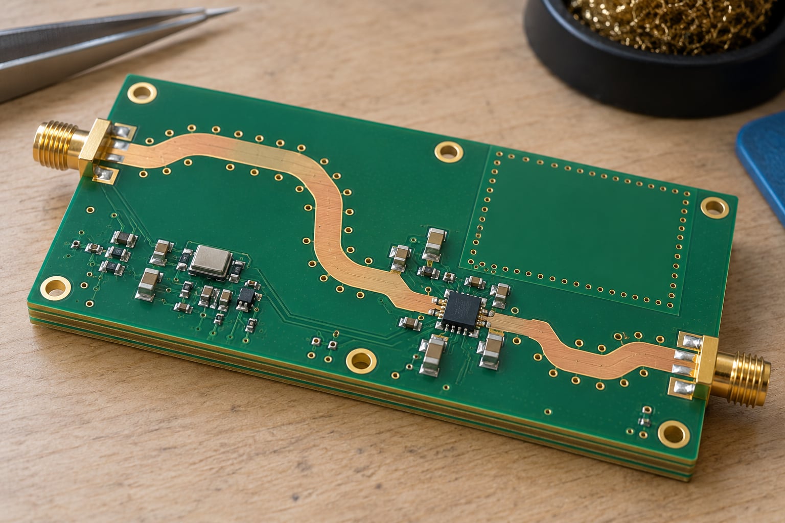
Widths come from the impedance target, the stackup and the calculator, not from habit. Once a width is computed, keep that net class on that width and do not mix geometries on the same line. A trace that is microstrip for part of its run and coplanar waveguide for the rest is two different transmission lines with two different impedances, and the junction between them reflects.
Bends are the next rule. Use 45-degree pairs or a proper arc rather than a right angle, and keep the bend radius at least three times the trace width. The right-angle story is usually told with a water pipe, which is a decent mental model: a sharp corner makes the signal take the outside path on the way in and the inside path on the way out, and the difference in length radiates.
At layer transitions, use two vias rather than one where you can, symmetric and close together, and add a ground via beside them. Two vias cut the inductance variation of the transition by roughly half compared with a single via, and they spread the parasitic capacitance more predictably. A via that punches through a plane without a nearby ground via leaves a stub of plane that can resonate. Where you must cross a digital signal with an RF signal, cross on adjacent layers and at right angles so the coupling area stays small.
Finally, keep RF traces short. Every millimetre is loss and every millimetre is a chance to pick up interference, and length also matters when the trace is close to a resonant dimension. If a matching network is needed, place it close to the antenna feed, not at the IC.
Check: every RF net is one geometry, one width, one reference plane, with bends and layer changes following the rules above.
6. Add Protection, Test Points, and Manufacturing Details
Protection comes first because it changes the layout. If the board has an external connector exposed to the user, put the ESD protection at the connector, not at the IC it protects, so the surge is diverted before it travels across the board. The principle behind component-level protection is covered in ESD protection in chip design explained if you want the device-level background.
Test points decide whether you can debug the board. Put a calibrated port or a short launch footprint on the antenna feed and on key nodes, and make sure each one has a proper ground reference nearby so a probe does not float. Keep the DC blocking capacitor and any bias tee in the RF path short, and remember that a DC block that is not actually blocking DC will bias the antenna or the front end unpredictably.
For the mechanical and assembly side: put ground pads under ICs and stitch them with through-hole thermal vias to move heat and to give the pad a low-inductance connection. Use thermal relief on the pad rather than a full pour, so the part still reflows properly. Add silkscreen identifiers that are actually legible at assembly, keep component spacing clear of tall parts so the board can be populated, and add mounting holes with their own clearance rather than letting them land on a plane edge.
Check: the board can be probed at the antenna feed and at each supply rail without removing components.
7. Validate the Design Before Fabrication
This is the step most first-time RF designers skip, and it is the one that decides whether the first spin works. The recurring question on RF design forums is some version of “how do I know this will function before I pay for boards?”, so here is a review sequence that answers it.
- Re-read the requirements against the layout. Every frequency, impedance and connector from your requirements sheet should be traceable to something in the design.
- Run design rule checks for clearance, width, annular ring, drill-to-copper and solder mask, and read the violations rather than dismissing them.
- Run a field solver on every RF net and compare the calculated impedance against your target. A 10 percent error is the difference between a board that works and one that does not.
- Extract layout parasitics — via inductance, pad capacitance, trace length and coupling — and re-simulate the chain with them included. Layout changes the circuit, so a design that was comfortable on paper can be marginal after extraction.
- Send the files for DFM review and ask the fabricator to confirm the stackup, the impedance tolerance and any keep-out or antenna handling requirements.
- Plan the measurement. Decide in advance which instrument you will use, what fixture you need and what a pass looks like. A VNA gives return loss and insertion loss directly; a TDR gives impedance along the trace.
After the boards arrive, measure before you power anything up. A TDR sweep of a 50 ohm line should read flat. If it does not, the problem is in the fabrication or the stackup, not in your circuit, and now you know that in an afternoon instead of a week.
Check: the field solver agrees with the target on every RF net, the DFM report is clean, and you have written down what you will measure on the first board.
Common RF PCB Design Mistakes
These are the errors that show up again and again, with the correction that actually fixes each one. Every item below is one of the failures these rf pcb design guidelines for beginners are built to prevent.
Using 1.6 mm FR-4 at 7 GHz. The board thickness sets the substrate height for a two-layer microstrip, and 1.6 mm of lossy FR-4 is a poor combination at that frequency. A thinner, lower-loss laminate with a controlled stackup is the right move, or move the design to a lower band.
Splitting the ground plane to separate analog from digital. The return current has to go somewhere, and forcing it through a capacitor or a narrow bridge raises the loop area. Keep one continuous plane and control coupling with spacing and via fences instead.
Mixed trace widths and geometries across one RF net. Every geometry change is an impedance discontinuity. Pick one width per net class and let the net class constraint do the work.
Using a via as a filter or a resonator. A via that is not accompanied by a nearby ground via leaves a plane stub that can ring at RF. Add the ground via, and use via pairs at layer transitions.
Placing a matching network at the IC instead of at the antenna. The network needs to see the antenna’s impedance environment, not the amplifier’s.
Right-angle bends and long parallel runs next to noisy nets. Use 45-degree pairs or arcs with a radius of at least three times the trace width, and keep spacing from switching and high-current circuitry.
Skipping the pre-fabrication check. This is the expensive one, because it is the mistake that costs a whole spin of boards. A field solver pass and a DFM review take an afternoon.
Confusing RF ground with DC ground. They are the same net electrically, but they behave differently. The RF return path is a controlled-impedance structure, and treating it as a generic net in the schematic is how the return-path rules get violated in layout.
Frequently Asked Questions
Is FR-4 good enough for RF, or do I need Rogers?
For most first RF boards, yes. FR-4 is generally usable to about 6 GHz and handles 2.4 GHz Wi-Fi and sub-GHz links comfortably, as long as you keep the stackup controlled and the traces short. Move to a Rogers-class laminate such as RO4003C or RO4350B when you need a tighter dielectric constant, a lower loss tangent, or when your highest frequency is well above 6 GHz. The material does not rescue a layout with a broken return path.
How many PCB layers do I need for RF?
Four layers is the practical answer for most designs: signal on top, a solid ground plane directly beneath it, then power and signal below. Two layers can work, but the whole board thickness becomes your substrate height, so keep it thin, roughly 30 mils or less, and expect the impedance to be approximate. One layer cannot provide a continuous return path, so it is not a real option. Eight layers only helps on a board that also carries fast digital signals.
Why do I need a ground plane under an RF trace?
Because the trace and the plane together form a transmission line, not a wire. An electromagnetic field surrounds the trace and return current flows in the adjacent plane along the field lines. The pair behaves as a capacitor, and their geometry sets the characteristic impedance. If the plane is missing or split, the return current detours, the loop area grows, inductance and radiated emissions increase, and the impedance you calculated is no longer the impedance your signal sees.
What is the difference between microstrip and stripline?
A microstrip trace sits on the outer layer with the reference plane below it, so its fields are partly in air, which makes it easy to access for probing and tuning but slightly less shielded. A stripline runs between two planes, which gives better confinement and shielding but requires a via to reach and makes probing harder. Both are impedance-controlled geometries, and the trace width, the dielectric thickness and the dielectric constant set the target in both cases.
How do I verify my RF PCB layout before fabrication?
Run a field solver on every RF net and compare the result against your target impedance, then extract layout parasitics and re-simulate the chain with via inductance and pad capacitance included. Send the files for a DFM review and ask the fabricator to confirm the stackup and impedance tolerance. Decide in advance what you will measure on the first boards, usually a TDR sweep for impedance and a VNA for return loss, so the acceptance criteria are written down before you spend anything.
How do I choose a trace width for 50 ohm?
You do not choose it by habit, you compute it. The width depends on your laminate dielectric constant, the thickness of the dielectric between the trace and its reference plane, the copper thickness, and whether the design has solder mask over the trace. Use a conformal-mapping calculator for a first pass, then confirm with a field solver that accounts for the real geometry. A single width that works on one stackup is simply wrong on another, which is why stackup is decided before routing.
Conclusion
The first thing to do is write the requirements down and pick a stackup your fabricator can actually build, because every trace width, every bend and every return path follows from that pair. Then draw the return paths before you place a single RF component, and run a field solver on the result before you order anything. These rf pcb design guidelines for beginners are only worth anything if the check at the end of each step is actually performed.