
Design rule checking is the automated process of testing a chip or board layout against the manufacturing rules of the process it will be built on, so every metal line is wide enough, far enough from its neighbour, and connected in a way the equipment can actually reproduce.
Beginners usually meet DRC after they have drawn their first few shapes in a layout editor and something looks slightly off. This guide walks through what the check really does, where the rules come from, what each rule type means, and how to read a report without panicking at the violation count.
Table of Contents
- What Is Design Rule Checking?
- Why Do Semiconductor Designs Need DRC?
- How Does Design Rule Checking Work?
- What Design Rule Checking Explained for Beginners Means in Practice
- Design Rule Checking Explained for Beginners: A Simple Example
- What Are the Main Types of Design Rules?
- Basic rules versus advanced-node rules
- Which Tools Are Used for Design Rule Checking?
- How to Read DRC Violations and Fix the Layout
- Design Rule Checking in the Early Stages of a Design
- Common Beginner DRC Mistakes
- A Practical DRC Workflow for Your First Layout
- Frequently Asked Questions
- What are DRC and LVS?
- Why do we need a DRC run when everything is automated?
- What does DRC not check?
- What is a rule deck file in VLSI?
- How long does a DRC run take?
- Is PCB design rule checking the same thing?
- Conclusion: Start With the Rule Deck and One Simple Layout
What Is Design Rule Checking?
Design rule checking is a set of geometric constraints that a layout must satisfy, and a software pass that tests the layout against every one of those constraints and reports the ones it fails. Nothing about it is circuit theory. It is geometry against a rulebook.
Think of the layout as a printed drawing and the rule deck as the print shop’s specification sheet. If two lines on the drawing are closer together than the press can resolve, the shop prints them merged. A DRC tool finds every place where the drawing asks for something the process cannot deliver, before the drawing is ever sent to press.
Where those rules come from matters as much as what they say. The fabrication line has a real physical limit on how tightly it can place two metal lines, and the foundry measures that limit on test wafers. The number that comes out of those measurements becomes a rule, and a few thousand of them together become a rule deck.
A handful of terms show up constantly, so it helps to fix their meanings before going further.
| Term | What it means |
|---|---|
| Layout | The physical drawing of the chip: polygons, paths and vias on numbered metal layers, with no circuit meaning attached. |
| Via | A vertical connection between two metal layers. It is a metal plug with a required size and a required amount of surrounding metal on both layers. |
| Rule deck | The machine-readable file of foundry rules. It is the single source of truth for a DRC run, and it is versioned. |
| Design Rule Manual | The human-readable document that accompanies the deck, with a diagram and a prose explanation for every rule. |
| Runset | Your selection of which layers and which rules to check, plus the switches controlling how the engine behaves. |
| Fill | Dummy metal added to a layer to balance its density across the die, so etching behaves consistently. |
| Tapeout | The release of the final layout database to the foundry for mask generation. There is no cheap way back. |
| Signoff | The stage where a design is declared ready for manufacture because every required check has passed. |
One more distinction catches people early. A rule check is a manufacturing check. It says nothing about whether the circuit you drew is the circuit you intended.
Why Do Semiconductor Designs Need DRC?
DRC exists because photolithography is not a perfect printer. A mask pattern is shrunk onto a resist, the resist is developed, and metal is deposited and etched, and every one of those steps introduces variation that the process engineers have to allow for.
Consider two metal traces on the same layer running parallel, separated by less than the process’s minimum spacing. In the scanner’s output, light meant for one trace partially exposes the gap next to it. In a dense region, the deposited metal touches when it was not supposed to. That is a short between two nets, and it may well be intermittent.
That single spacing error produces three different problems at once, which is why spacing rules exist in the first place.
| Rule | Physical problem it prevents | What you see on silicon |
|---|---|---|
| Minimum spacing | Two features merge during patterning or etch | An unintended short, sometimes only on some die |
| Minimum width | A thin line is printed wider than drawn, or breaks up entirely | Resistance drift, or an open connection |
| Minimum area | Small isolated islands of metal are hard to hold and hard to etch | Disappearing vias, poorly defined contacts |
| Enclosure | A via lands near the edge of the shape it connects to | A high-resistance or missing connection |
| Extension | A transistor’s source or drain metal stops short of the gate edge | Extra contact resistance, leakage between devices |
| Antenna | Charge builds up on a gate during a plasma step and tunnels through the oxide | A shifted threshold voltage on a matched device |
| Density | Large open areas of metal etch differently from dense areas | Uneven critical dimensions across the die |
Beyond the electrical failure, there is the schedule failure. A chip that comes back from the foundry with a defect is a respin, and a respin is months of schedule and a large slice of the project’s budget. DRC is the last cheap place to catch all of this.
How Does Design Rule Checking Work?
A DRC engine does one thing repeatedly: it takes every shape on every enabled layer, and tests it, and tests it against every other shape nearby, against the rules in the deck. Anything that fails becomes a violation record with a location and a rule name.
That loop is worth understanding, because it explains the two things beginners find strange about DRC. First, the report can be enormous, because a single wide rule applied to a full chip finds thousands of candidate pairs. Second, the tool has no idea which of those pairs matter, so it reports them all and leaves the judgement to you.
Newer engines accelerate that pair search with spatial indexing, so shapes far apart on the die are never compared. The result is close to linear with area rather than quadratic, which is the only reason a full-chip run is practical at all.
What Design Rule Checking Explained for Beginners Means in Practice
In practice, design rule checking explained for beginners comes down to four inputs and one output. The inputs are your layout database, the foundry’s rule deck, the runset that selects layers and rules, and the tool’s database-grid scale setting. The output is a report of failed rules and a marker on the offending geometry.
Change any one of the four and the output changes. That is why a run that suddenly returns ten thousand errors is usually a configuration problem rather than a design problem, and checking the deck and the settings first saves a lot of wasted editing.
Design Rule Checking Explained for Beginners: A Simple Example
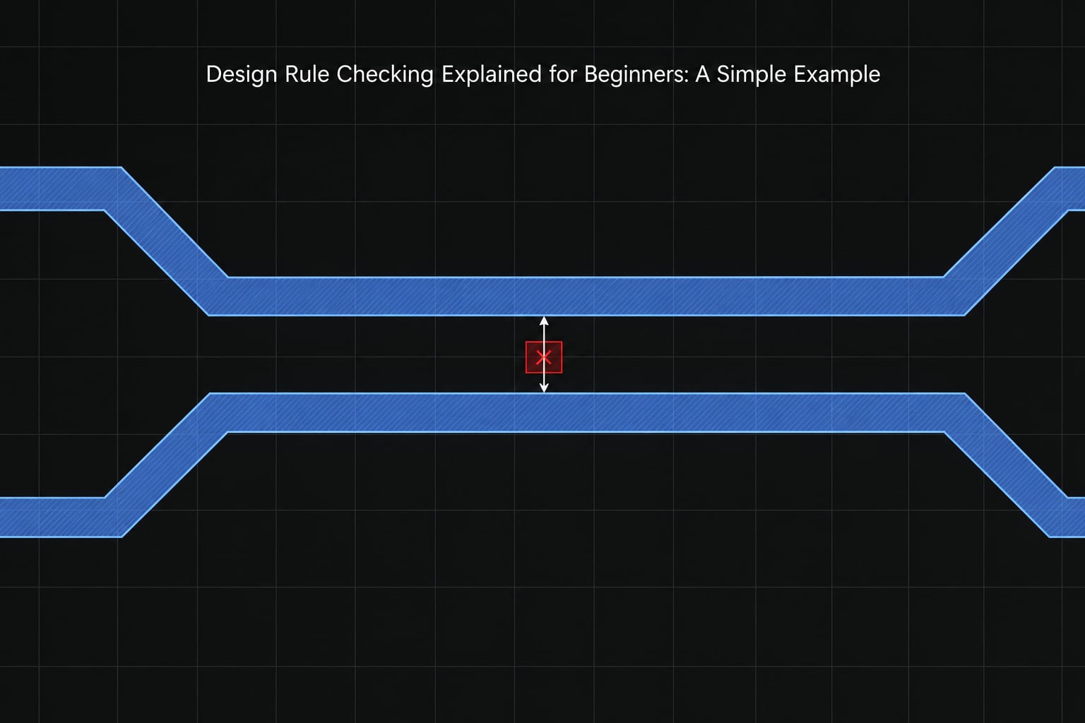
Here is the smallest useful example. Take two parallel shapes on metal 1 with 40 nanometres of space between them, on a process whose minimum spacing for that layer is 60 nanometres.
The engine compares the two shapes against the spacing rule, measures the gap at 40, and records a violation at the point on the boundary closest to the other shape. The report entry typically names the rule, the layer, the two coordinates, and the measured value against the required value.
Metal1.spacing          ( 12.400, 88.150 )  ( 12.400, 88.190 )
  measured 0.040 um   required 0.060 um   delta 0.020 um
Now the part beginners skip. The fix is not to squeeze the tool’s threshold. The fix is to change the layout so the gap is genuinely larger, by moving one shape, by shifting a neighbouring route, or by inserting a jog if the design has the room for one.
Then you re-run. The reason for the re-run is that moving a shape frequently creates a new problem a few millimetres away, such as a via that no longer has enclosure on one side, and only a fresh run tells you so.
What Are the Main Types of Design Rules?
Rule decks group their checks into recognisable families. Learning these names is most of what reading a report requires, because the rule name tells you which family the error belongs to.
| Rule type | What it constrains | Typical violation message |
|---|---|---|
| Minimum width | No drawn feature may be narrower than the process can hold | Metal1 width too small |
| Minimum spacing | No two features on one layer may be closer than the process resolves | Metal1 spacing too small |
| Minimum area | Small isolated shapes are unreliable and are not allowed | Metal1 area below minimum |
| End-of-line spacing | The gap at the end of a line needs more room than the gap along it | Metal1 end-of-line spacing |
| Space at a notch | A concave corner behaves differently from a straight edge | Notch spacing violated |
| Wide metal jog | A wide shape must taper rather than step abruptly | Wide metal jog rule |
| Via enclosure | A via must sit fully inside the metal shapes on both layers | Via1 enclosure on Metal1 |
| Via-to-via spacing | Adjacent vias merge or etch unevenly when packed too tightly | Via1 spacing too small |
| Extension | Source and drain metal must extend past the device edge by a defined amount | Poly extension below minimum |
| Misaligned via wire | A via landing at a layer change must sit under a sufficiently wide shape on both layers | Misaligned via wire |
| Antenna ratio | The area of connected metal above a gate must stay within a multiple of the gate area | Antenna ratio exceeded on Net name |
| Density | Metal coverage must fall inside a window, both overall and in every window | Metal1 density outside limits |
Basic rules versus advanced-node rules
What most people mean by base DRC is the geometric set above: width, spacing, area, enclosure, extension. These are still checked everywhere, and on a mature node they are usually the only rules you will see in a beginner project.
As nodes shrink, three more families arrive. Contextual rules ask whether a feature is legal given its surroundings, such as a notch inside a dense region. Density and fill rules demand metal coverage inside a window and require dummy structures where the coverage is low. Multi-patterning rules then check that coloured regions which are meant to print separately do not collide, which adds checks that are topological rather than dimensional.
The practical consequence for a beginner is that a deck is not a fixed list. A foundry’s deck for a leading-edge node can hold several times the rules of a mature one, and the same geometry can be legal in one deck and illegal in another.
Which Tools Are Used for Design Rule Checking?
Three commercial families dominate chip DRC, and they are usually described by role rather than by version, because the engines differ more in workflow than in output. Synopsys IC Validator is widely used in large ASIC and design-for-manufacturability flows. Cadence PVS and Assura are common in analog and custom layout work. Siemens Calibre is used across both, and for foundry-qualified signoff decks.
Board-level DRC is a different world with a different vocabulary. Altium Designer, KiCad and similar tools check trace width, copper-to-copper clearance, solder mask slivers, board-edge keepout and annular ring around drilled holes. The acronym is identical and the underlying idea is the same, but the rule numbers come from IPC standards and your fabricator rather than from a semiconductor process.
Open-source options exist for learning. Magic, developed originally for the Magic VLSI project, performs DRC and layout work in an open environment. KLayout can read GDS and run checks through scripting, and it is genuinely usable as a first layout viewer and rule checker for a student.
Whichever tool you use, the loading sequence is the same. You point it at the layout database, you point it at the rule deck the foundry published for your exact process and layer stack, and you load a runset that matches the corner and the option the design is signed off for.
How to Read DRC Violations and Fix the Layout
Reading a report well is mostly a fixed order of operations. The report is a list of failed rules, and the job is to turn each entry into a physical edit.
1. Locate the marker. Every violation carries a layer and an x,y coordinate. Jump the editor to that point before reading anything else, because the geometry tells you more in two seconds than the rule name does in ten.
2. Read the rule name against the deck. Codes like M1.S.2 or VIA1.ENCLOS are not self-explanatory. Look the code up in the Design Rule Manual, where each entry has a diagram and states the required value and the layer pair it applies to.
3. Identify the physical cause. Spacing, width, enclosure and extension each fail in one of a few shapes: a corner is too close, a stub is too short, a via sits on a boundary, or two long lines ran parallel for longer than the rule allows.
4. Make the smallest edit that fixes the cause. Widening a line to clear a single spacing error often creates an enclosure error on an adjacent via, and the cascading is the reason editing too eagerly is expensive.
5. Re-run before reading the next entry. DRC reports are only meaningful at the state of the database when the run started. A stale report sends people chasing errors that no longer exist, which is the single most common way beginners lose a day.
Not every error is equally serious. A missing enclosure on a signal via is a real defect risk. A density window on a metal layer that is fully covered by fill is often cosmetic. The rule severity in the deck, and the waiver process the foundry offers, exist precisely because these cases are different.
Design Rule Checking in the Early Stages of a Design
DRC is not a single event before tapeout. It runs repeatedly through the flow, and the run you do changes depending on the stage.
Before routing, the useful check is a partial run over the coarse geometry already placed, with fill excluded and the more expensive contextual rules switched off. It runs in minutes and catches gross spacing problems while they are still cheap to move.
After routing, a full run over all signal layers with the real runset is the working check. This is where most of the fixing happens, because routing is where wires end up close together and where vias pile up.
At signoff, the run uses the foundry’s exact deck version, the exact corner, and the exact options for that die, with no rule waived that the foundry has not agreed to waive in writing. Runtimes here can stretch into hours on a large design at an advanced node, which is why teams schedule the run early and read the results the same day.
That growth is not a tool inefficiency. Rule count climbs steeply as nodes shrink, each rule costs more to evaluate, and the added checks for fill, density and patterning decomposition are precisely the ones that touch the whole die. A schedule that assumes DRC is instant will be wrong at signoff, and the earlier you accept that, the less it costs.
Common Beginner DRC Mistakes
Most beginner DRC problems are not geometry problems. They are setup and expectation problems, and they repeat.
Using the wrong deck version. A foundry updates its rules between lots. Running an older deck produces a clean result that the fab will not honour, which is a worse failure than a visible error because nothing flags it.
Checking an incomplete layer set. Running DRC on the layers you happen to be editing rather than the full stack gives a false clean signal, because a via error only appears when both connected layers are enabled.
Confusing the database grid with the tool’s scale setting. Layout databases are stored on a fine internal grid, and a run configured to read those coordinates as microns reports a full chip of impossible errors, which wastes more time than any other beginner mistake.
Ignoring repeated violations. The same rule failing two hundred times usually means one structural decision, such as a router setting or a channel that is too narrow, rather than two hundred separate mistakes. Fix the cause once.
Breaking one rule to fix another. Widening a shape to solve spacing can immediately violate enclosure or density. Every edit gets a re-run, or the fix order stops being meaningful.
Treating every error as fatal. Density and fill messages in particular are often about a window that a later fill step will resolve. Learn which families are hard failures in your process and which are advisory.
Working from a stale report. A report describes the database as it was when the run started. This is the fastest way to waste an afternoon on errors that no longer exist.
A Practical DRC Workflow for Your First Layout
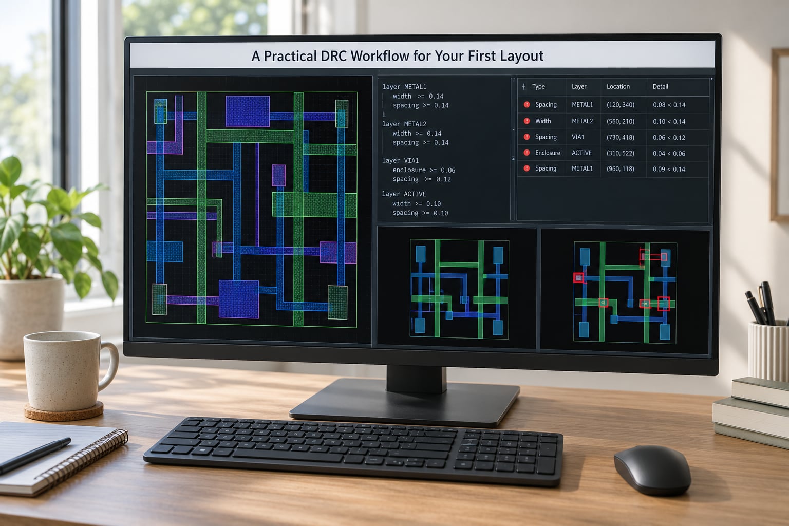
Here is the sequence I would hand a beginner, in order.
1. Obtain the correct rules. Ask the course provider or foundry for the rule deck and the Design Rule Manual that match your process, and confirm the layer names in the deck match the layer names in your editor. Nothing else in this list works without this.
2. Define the layers. Map your design’s layers to the deck’s names, and enable every layer your design actually uses, including the layers that only carry fill or power.
3. Confirm the scale. The database is drawn on a fine internal grid, and a run configured to read that grid as if it were microns reports a full chip of impossible errors.
4. Run a partial check first. Start with a few layers and the basic geometric rules, get that report clean, and only then widen the runset. Adding layers one at a time keeps the error count interpretable.
5. Inspect and fix in order. Group the report by rule family, look up the code in the manual, and fix the highest-count structural cause first, because it usually removes many of the rest.
6. Re-run and record. Repeat until the run returns nothing, and note the deck version and runset used so the next person, including future you, can reproduce the result.
If you have no foundry access at all, you can still learn the workflow. Run an open-source checker on a small test layout with a sample deck, fix what it reports, and you will be practising exactly the skill the real flow needs.
Frequently Asked Questions
What are DRC and LVS?
DRC compares your layout’s geometry against the foundry’s manufacturing rules, answering whether the chip can be built. LVS compares the layout’s extracted devices and nets against the schematic netlist, answering whether the chip is the circuit you intended. They fail for different reasons: DRC catches spacing, width, enclosure and antenna problems, while LVS catches shorts, opens and device mismatches. A design must pass both before tapeout, and neither one substitutes for the other.
Why do we need a DRC run when everything is automated?
Because automation optimises for timing, area and routing completion, not for every geometric constraint in the deck. Place-and-route tools respect the rules they are configured with, on the layers they are configured to see, and they work within the margins their algorithms were tuned for. A final DRC run uses the exact foundry deck, the exact corner and the full layer stack, and it is a mandatory signoff gate that a human signs. That is why it is never skipped, even on a fully automated flow.
What does DRC not check?
DRC does not check whether your circuit works. It does not verify connectivity against the schematic, which is LVS’s job, or electrical rules such as voltage domains, current density and electromigration, which are ERC and reliability checks. It also cannot tell you that a design is wrong in a way no rule describes, such as a mirrored device or a swapped pin. Treat a clean DRC as one necessary condition, not as evidence of correctness.
What is a rule deck file in VLSI?
A rule deck is the machine-readable file that encodes a foundry’s manufacturing constraints for one process and layer stack. The tool reads it to know which checks to run and what values to enforce, and the version you sign off with must match the version the foundry will build to. A foundry normally publishes it alongside a human-readable Design Rule Manual, which gives a diagram and explanation for every rule code. The deck and the manual should always be read together.
How long does a DRC run take?
It depends on three things: the area being checked, the number of layers enabled, and the rule count of the deck. A partial run over a few layers can finish in minutes, while a full-chip signoff run on a mature node might take a few hours. At leading-edge nodes the same design can take much longer, because rule count rises steeply and contextual, density and patterning checks are expensive. Treat runtime as a scheduling input rather than assuming it is instant.
Is PCB design rule checking the same thing?
The idea is the same, the numbers are not. Board-level DRC checks trace width, copper clearance, solder mask slivers, annular ring and board-edge keepout against IPC standards and your fabricator’s capabilities. Chip-level DRC checks nanometre-scale spacing, width, enclosure, antenna and density rules from a semiconductor rule deck. The acronym means different things to the two audiences, so when you search or ask for help, say which one you mean.
Conclusion: Start With the Rule Deck and One Simple Layout
If you remember one thing from this guide, make it this: the first action is not drawing more layout. It is getting the correct rule deck and the Design Rule Manual that match your process.
Then run the check on one small test structure, read the report, look up the rule code, and fix the geometry. Repeat until that run is clean. Design rule checking is not something you read about once; it is a loop you repeat until the report is empty, and that loop is the whole job.