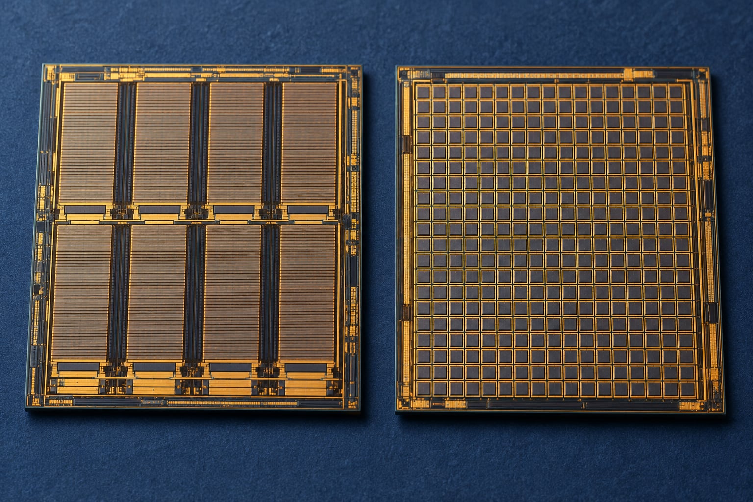
The core difference is how the memory cells are wired. NAND strings its cells in series for high density and low cost per bit, so it reads and writes by page. NOR wires its cells in parallel to the bit lines, so it reads at byte level and runs code directly from the chip. Pick NOR for code and small data regions; pick NAND for capacity.
Here are the nand flash vs nor flash differences explained across architecture, timing, endurance, density, power and application, so you can match the memory type to the workload instead of guessing from datasheet marketing.
Table of Contents
- NAND Flash vs NOR Flash Differences at a Glance
- How NAND and NOR Flash Store Data
- NAND architecture: the cell string and page buffer
- NOR architecture: parallel cells on the bit line
- Reading, Writing, and Erasing: NAND vs NOR
- Speed and Latency
- NAND flash vs NOR flash differences in read and write speed
- Endurance, Data Retention, and Failure Behavior
- Density, Cost, and Scalability
- Power Consumption and System Design
- NAND Flash vs NOR Flash: Which One for Common Use Cases?
- NAND Flash vs NOR Flash Differences Explained by Example
- A microcontroller bootloader
- A camera firmware update
- A high-capacity storage appliance
- Common misconceptions worth clearing up
- How to Choose the Right Flash Memory
- Frequently Asked Questions
- Is NAND flash faster than NOR flash?
- Which flash memory is better for firmware: NAND or NOR?
- Why does NOR flash cost more per bit than NAND flash?
- Can NAND flash replace NOR flash in a microcontroller design?
- Is NAND or NOR flash more reliable for long-term storage?
- What is the main difference between page, block, and sector erase operations?
- Conclusion
NAND Flash vs NOR Flash Differences at a Glance
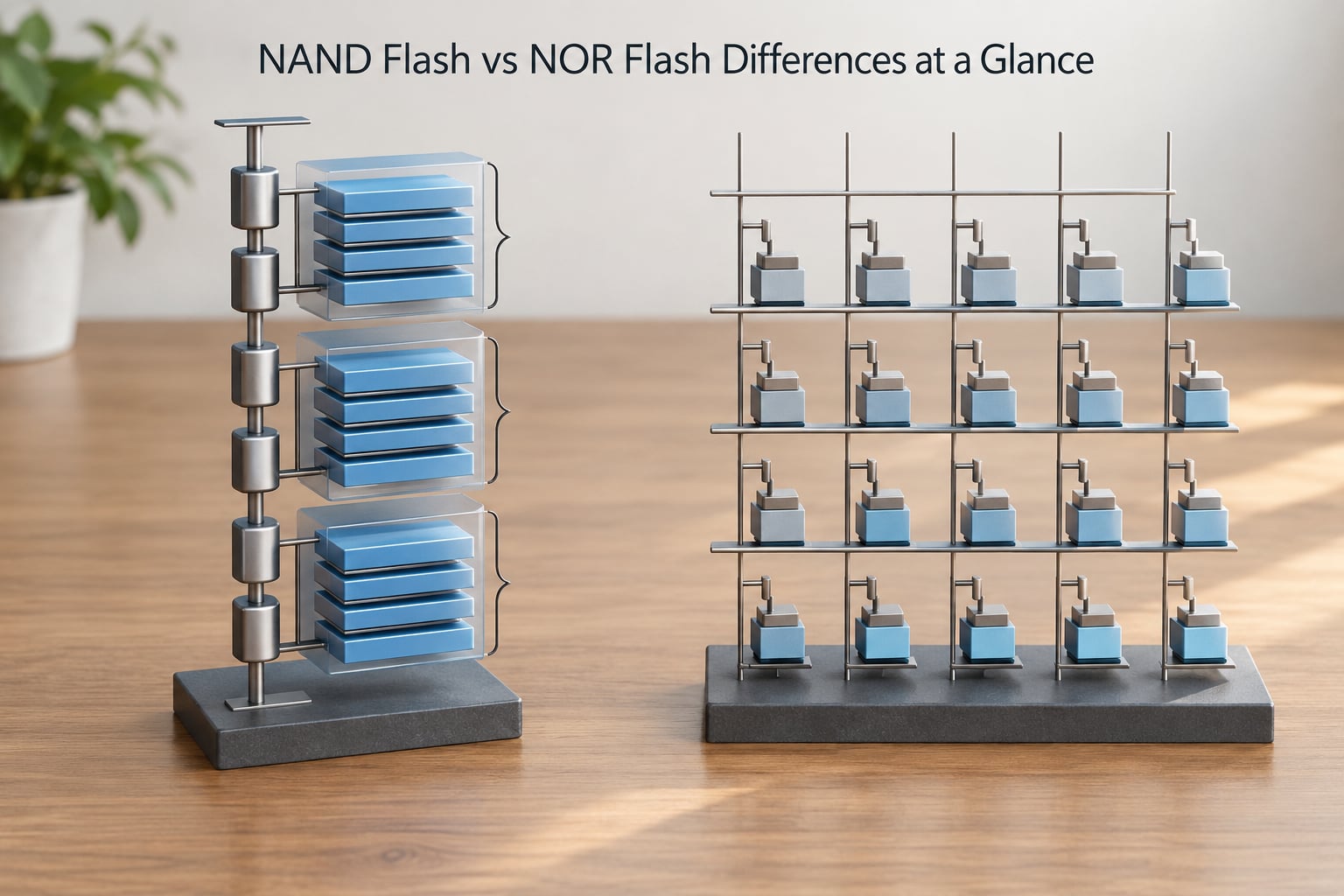
Read this table first. Everything after it is the reasoning behind these numbers.
| Attribute | NAND flash | NOR flash |
|---|---|---|
| Cell connection | Cells in series along a shared bit line | Each cell connected in parallel to its bit line |
| Named after | The NAND logic gate arrangement | The NOR logic gate arrangement |
| Read unit | Page, through a page buffer | Single byte or word |
| Access style | Command-driven, multiplexed address and data bus | Random access, reads like asynchronous SRAM |
| Program unit | Page or partial page | Byte or word |
| Erase unit | Block (or large sector) | Sector, typically 4KB to 64KB |
| Erase before write | Required on the containing block | Required on the containing sector |
| Random read latency | Tens of microseconds, page must be loaded first | Tens to hundreds of nanoseconds |
| Sequential read throughput | Faster once a page is loaded, wins above roughly 1KB of contiguous data | Flat, good but not improving with length |
| Erase time (large chunk) | A few milliseconds per block | Hundreds of milliseconds for the same byte count |
| Code execution | Not direct from raw NAND; copied to RAM or handled by an embedded controller | Execute-in-place supported on most devices |
| Typical density range | 1Gb to 16Gb and beyond | 64Mb to 2Gb |
| Cost per bit | Low | High, several times NAND at the same capacity |
| Program/erase endurance | Wide range, roughly 10^5 cycles for SLC down toward 10^3 for QLC | Typically 10^4 to 10^5 cycles |
| Error handling | Bad blocks shipped from factory, ECC or LDPC required | No factory bad blocks, no ECC needed for most designs |
| Interfaces | Raw parallel NAND, SPI NAND, eMMC, UFS | Parallel NOR, SPI NOR, QSPI NOR |
| Power profile | Short active bursts, low standby, notable erase current | Steady low read current, higher erase voltage and current |
| Best fit | Mass storage, large firmware images, data logging | Boot code, firmware, FPGA bitstreams, code storage |
How NAND and NOR Flash Store Data
Both types store a bit the same way at the transistor level. A floating-gate MOSFET carries an insulated gate that either holds or does not hold charge, and that charge shifts the transistor’s threshold voltage. Reads sense the threshold voltage, programming injects charge, and erase removes it by pushing charge back through the oxide using Fowler-Nordheim tunneling.
Where they part ways is the wiring around that transistor. In NAND, dozens of cells share a bit line in series, with select transistors at each end and a sense amplifier reading the string. In NOR, every cell has its own connection to a bit line.
That single wiring decision cascades into everything else: how data is addressed, how many address pins you need, what the erase unit looks like, whether error correction is mandatory, and what a megabit costs.
NAND architecture: the cell string and page buffer
A NAND page is the read and program unit, typically 2KB to 16KB of user data plus a spare area used for ECC and metadata. To read, the controller issues a page-read command, loads the whole page into the on-die page buffer, then streams it out. Pages are grouped into blocks, and the block is the erase unit.
NOR architecture: parallel cells on the bit line
In NOR, each bit line runs independently to its own cell, so any address can be selected without touching its neighbours. Engineers on TI’s E2E forum describe reading from NOR directly like asynchronous SRAM. That SRAM-like behaviour is exactly why a processor can boot straight into NOR.
Reading, Writing, and Erasing: NAND vs NOR
Reading differs sharply. NAND needs the page loaded into the buffer first, so a random access costs the whole page-load. NOR addresses any cell directly on the bus, so a random read costs almost nothing extra.
Writing in NAND is page-based and can only lower bit values within a programmed page; raising them back requires an erase. NOR programs a byte or word in place, but the same erase-before-rewrite rule applies at sector level.
Erasing is where the two part company most. NAND erases a whole block, typically hundreds of megabytes of user data per operation. NOR erases a sector, typically 4KB to 64KB. Both erase slowly relative to a program operation because removing charge requires holding a high field across the oxide, and a practitioner on Electronics Stack Exchange put it plainly: block erase on the order of milliseconds, one order of magnitude above write.
One terminology trap catches people coming from disk drives: in NOR a sector is a physical erase unit, while in NAND a sector is usually a logical convention inherited from the 512-byte disk model. NOR has no true page concept at all; block and page are effectively synonymous.
Speed and Latency
The honest answer is that neither type is universally faster. It depends on what you measure.
NAND flash vs NOR flash differences in read and write speed
For random single-byte access, NOR wins by a wide margin. Datasheet figures from the same generation of parts put NAND random read around 30 microseconds against NOR at roughly 120 nanoseconds, a difference of about 250 times. NOR behaves like a fast ROM; NAND behaves like a paging device.
For sequential reads the ordering flips. Once a NAND page is resident in the buffer, transferring contiguous data is efficient, and past roughly 1KB of contiguous transfer NAND throughput overtakes NOR. This crossover is the most commonly repeated mistake in comparisons: for streaming a large image, NAND is the faster device.
Erase shows the largest absolute gap. The same published comparison puts a 128KB erase at about 3.5ms in NAND against roughly 520ms in NOR, around 150 times slower for NOR, because NOR must erase a much smaller sector to clear the same number of bytes.
Real numbers on your board come from the controller, the interface, the page size and the driver, not from the cell array. Two devices with identical NAND can differ by an order of magnitude once you include ECC time, wear-levelling metadata and the host protocol.
Endurance, Data Retention, and Failure Behavior
Endurance is measured in program/erase cycles per block or sector. It is not a fixed property of NAND or NOR alone; it depends on how many bits each cell stores, which is where the cell taxonomy matters.
NAND spans roughly 10^5 program/erase cycles for SLC down toward 10^3 for QLC. NOR parts typically sit in the 10^4 to 10^5 range, and buffer programming on modern devices helps by programming a page in one pass rather than touching bits individually.
The old claim that NAND has roughly ten times the endurance of NOR no longer holds broadly. It depended on a generation of parts, and the gap has narrowed or reversed depending on which NAND cell type and which NOR part you compare.
Failure behaviour differs more than the endurance numbers do. NAND ships with factory-marked bad blocks that the flash translation layer never uses, and bit errors appear as you approach the program/erase limits, so ECC or LDPC is part of the design rather than an option. NOR parts ship with every location usable, and read errors in the field usually trace to more than 10^4 erase cycles on a sector. Practitioners on r/ECE describe NOR as markedly more stable and less prone to error for exactly this reason.
Data retention is quoted in years at a given temperature, and retention falls as cells wear and as ambient temperature rises. Neither type holds data forever without a refresh policy on long-lived products.
Density, Cost, and Scalability
NAND wins density because series-connected cells need one bit line per string instead of one per cell. That is why NAND scales into gigabits while NOR stalls in the hundreds of megabits, and why cost per bit falls as capacity rises.
Higher density within NAND comes from storing more bits per cell. That single decision trades endurance for capacity.
| Cell type | Bits per cell | Typical P/E cycles | Common use |
|---|---|---|---|
| SLC | 1 | 10^5 | Industrial, automotive, eMMC premium |
| MLC | 2 | 3,000 to 10,000 | Enterprise SSD, legacy designs |
| TLC | 3 | 500 to 3,000 | Consumer SSD, smartphones, UFS |
| QLC | 4 | 100 to 1,000 | Value SSD, high-capacity storage |
| PLC | 5 and above | Under 1,000 | Emerging, cold storage research |
NOR’s answer to the same pressure is packaging and process, not bit packing. NOR also benefits from shrinking geometries and stacked die, which is how large configuration devices exist at all.
Power Consumption and System Design
Standby current is low in both types, on the order of microamps, so a sleeping device is not where the difference shows up.
The interesting case is an active embedded system. NOR runs directly from the flash, so a microcontroller can boot, fetch its vector table and execute without copying firmware into external SRAM. That can remove an external memory chip and its board area entirely, which usually wins on total system power for a small device doing real work.
NAND needs more around it: a controller or FTL, ECC engines, a page buffer and typically more firmware to manage wear levelling and garbage collection. That overhead costs silicon area, boot time and engineering hours. For a device that only writes a log every few minutes, a low-duty-cycle controller with aggressive sleep modes keeps average power below what an always-resident NOR system draws.
Erase is the current spike in both, and NOR’s erase runs longer and needs a higher voltage, which is why board-level power budgets treat erase as an event to schedule rather than a steady cost.
NAND Flash vs NOR Flash: Which One for Common Use Cases?
The mapping is fairly clean once you ask what the data does.
| Use case | Recommended type | Reason |
|---|---|---|
| Microcontroller firmware and bootloader | NOR | Random reads and execute-in-place |
| BIOS and UFI firmware | NOR or on-chip flash | Fast update, low-latency boot path |
| FPGA configuration bitstream | NOR | Random address access during configuration |
| Router and IoT firmware | NOR for small builds, NAND or eMMC for large images | Capacity ceiling decides it |
| USB flash drive, SD card, SSD | NAND | Capacity and cost per bit |
| Smartphone and tablet storage | UFS or eMMC over NAND | Managed controller, high sequential throughput |
| Data logging and telemetry | NAND | Large append-heavy writes |
| Automotive infotainment | eMMC, NOR for boot | Split of code-execution and capacity roles |
| Hybrid boot plus data device | Both | NOR boots the NAND controller |
That last row is the pattern most modern designs settle on. The NOR holds a small bootloader that initialises the NAND controller and hands off, and everything else lives in NAND. It sidesteps both weaknesses.
Hybrid packages exist that combine both in one module, and eMCP puts an SPI NOR alongside managed NAND on the same substrate, which saves board space when firmware needs random access and data needs capacity.
NAND Flash vs NOR Flash Differences Explained by Example
Three scenarios make the tradeoffs concrete.
A microcontroller bootloader
A 64KB NOR device holds the bootloader. The CPU reads the reset vector, verifies an image and jumps, all with no RAM shadowing and no ECC engine in the firmware. Swap in raw NAND and you now need a page loader, a bad-block-aware block allocator and an ECC decoder before your device boots at all. For a boot path measured in milliseconds on battery power, NOR is the right call.
A camera firmware update
The update is a 40MB image. That exceeds practical NOR capacity, so it lands in NAND or eMMC. The cost is software effort: a resume-capable write routine, power-fail recovery, and verification after each chunk, because a failed update in the field means a return trip. Keeping the bootloader in NOR means a bricked main image can still be recovered.
A high-capacity storage appliance
Here everything is NAND. Capacity, cost per bit and sequential throughput dominate, and the sequential crossover means bulk streaming actually favours NAND. NOR never enters the design, because at this scale its cost per bit is prohibitive and its capacity ceiling is hit first.
Common misconceptions worth clearing up
Three claims come up repeatedly and all three are wrong. NOR is not always more durable; endurance depends on the cell type and part. NAND cannot run code; it can, once copied to RAM or with an embedded controller that handles execution. And a slower random read does not mean NAND is slower overall, once you account for the sequential crossover.
How to Choose the Right Flash Memory
Work through these in order. The first match decides the answer.
- Does the processor execute from this memory? If yes, choose NOR, or on-chip flash with the same characteristics.
- How large is the image or dataset? Above a few megabytes, NAND is the only realistic option.
- Is access random or sequential? Random byte access favours NOR; long sequential transfers favour NAND.
- How often do you erase? Frequent rewrites of the same region favour SLC-grade NAND with wear levelling, or NOR if endurance is the real constraint.
- What is your latency budget? Sub-microsecond random reads are NOR territory. Microsecond-scale is acceptable for most firmware paths.
- How much capacity do you need? Beyond roughly 2Gb of code-sized data, stop considering NOR.
- What is your power budget? If the device sleeps for weeks at a time, NAND with a low-duty-cycle controller can beat an always-powered NOR system.
- What interfaces does your part support? Most modern microcontrollers expose a QSPI controller that takes NOR directly and often SPI NAND as well, which can settle the decision on pin count alone.
- What is the environment? Industrial and automotive temperature ranges, and long retention requirements, push toward SLC NAND or higher-grade NOR.
- Can your team absorb ECC and bad-block management? If not, that is not a small cost. Choose NOR or a managed device such as eMMC.
One rule of thumb covers most designs: if the data is code that runs, use NOR. If the data is content that is stored, use NAND.
Frequently Asked Questions
Is NAND flash faster than NOR flash?
It depends entirely on the access pattern. NOR is roughly 250 times faster for random single-byte reads, since it addresses cells directly, while NAND must load a whole page first. For sequential reads above roughly 1KB of contiguous data, NAND wins, because throughput improves once a page is resident in the buffer. Judge the device on your workload, not on a single latency number.
Which flash memory is better for firmware: NAND or NOR?
NOR, in most embedded designs. It gives byte-level random access, execute-in-place code execution and no requirement for ECC, bad-block management or a flash translation layer. NAND becomes the better answer when the firmware image is large enough to exceed NOR capacity, or when you need large data storage alongside the code.
Why does NOR flash cost more per bit than NAND flash?
Because every cell in NOR needs its own connection to a bit line, while NAND connects cells in series and shares one bit line across a whole string. The parallel wiring consumes far more die area per bit, so yield is lower and cost per bit is higher. NOR also carries less density headroom, since it does not scale into gigabits the way NAND does.
Can NAND flash replace NOR flash in a microcontroller design?
Only with real software work. NAND cannot be addressed at byte level, so you need a boot stub that initialises the controller, loads a page at a time into RAM and jumps to it. You also need ECC decoding, bad-block avoidance and a wear-aware update path. Many designs do it, but they keep a small NOR bootloader so a failed main image can still be recovered.
Is NAND or NOR flash more reliable for long-term storage?
NOR is easier to make reliable because it ships with no bad blocks and normally needs no error correction, so a read either succeeds or reports a failure cleanly. NAND handles errors through ECC and bad-block management, which is effective but adds complexity and firmware. For archive-grade storage at scale, NAND wins on capacity; for a small critical code store, NOR is the simpler choice.
What is the main difference between page, block, and sector erase operations?
A page is the read and program unit, a block is the physical erase unit, and a sector is a term that means different things in the two types. In NAND, erasing a block clears every page in it, which is why rewriting one page can cost you a whole block of writes. In NOR, a sector is the physical erase unit itself, and no true page concept exists.
Conclusion
NOR wins where code runs from the memory: bootloaders, firmware, BIOS and UFI images, FPGA bitstreams. Its byte-level random access and execute-in-place behaviour mean a simple, reliable boot path with no ECC engine and no flash translation layer.
NAND wins where data simply has to exist: solid-state drives, memory cards, USB devices, managed storage such as eMMC and UFS, and any dataset past a few megabytes. Its series cell wiring delivers density, cost per bit and sequential throughput that NOR cannot approach.
Start your decision with four questions. What is the access pattern, how much capacity do you need, how often will you erase, and what does your power budget allow. The answers pick the type for you, and for most designs the hybrid of NOR for boot plus NAND for data is the answer that ages best.