Tapeout is the moment an integrated circuit design stops being a file and becomes something a factory can build. Until that point, every fix is cheap and reversible. After it, every mistake is on a photomask and repeats on every wafer the line makes.
The term confuses newcomers more than almost any other in the flow, usually because it is used loosely for three different things: the design milestone, the data handoff, and the mask-making order. Getting what tapeout means in chip design right means separating those three, then walking the stages, the files you submit, the timing, the cost drivers and what happens to first silicon.
Table of Contents
- What Tapeout Means in Chip Design
- How the Tapeout Process Works
- What Is Included in a Tapeout Package?
- Tapeout vs. Fabrication: Where Does the Boundary Fall?
- How Long Does a Tapeout Take?
- How Much Does a Tapeout Cost?
- What Happens After a Successful Tapeout?
- Common Tapeout Mistakes and How to Avoid Them
- Frequently Asked Questions
- What is the difference between tapeout and fabrication?
- Is tapeout the same as mass production?
- What files are sent to the foundry for a tapeout?
- How many tapeouts does a chip usually need?
- What should a chip designer check before tapeout?
- Does tapeout include packaging and final testing?
- Conclusion
What Tapeout Means in Chip Design
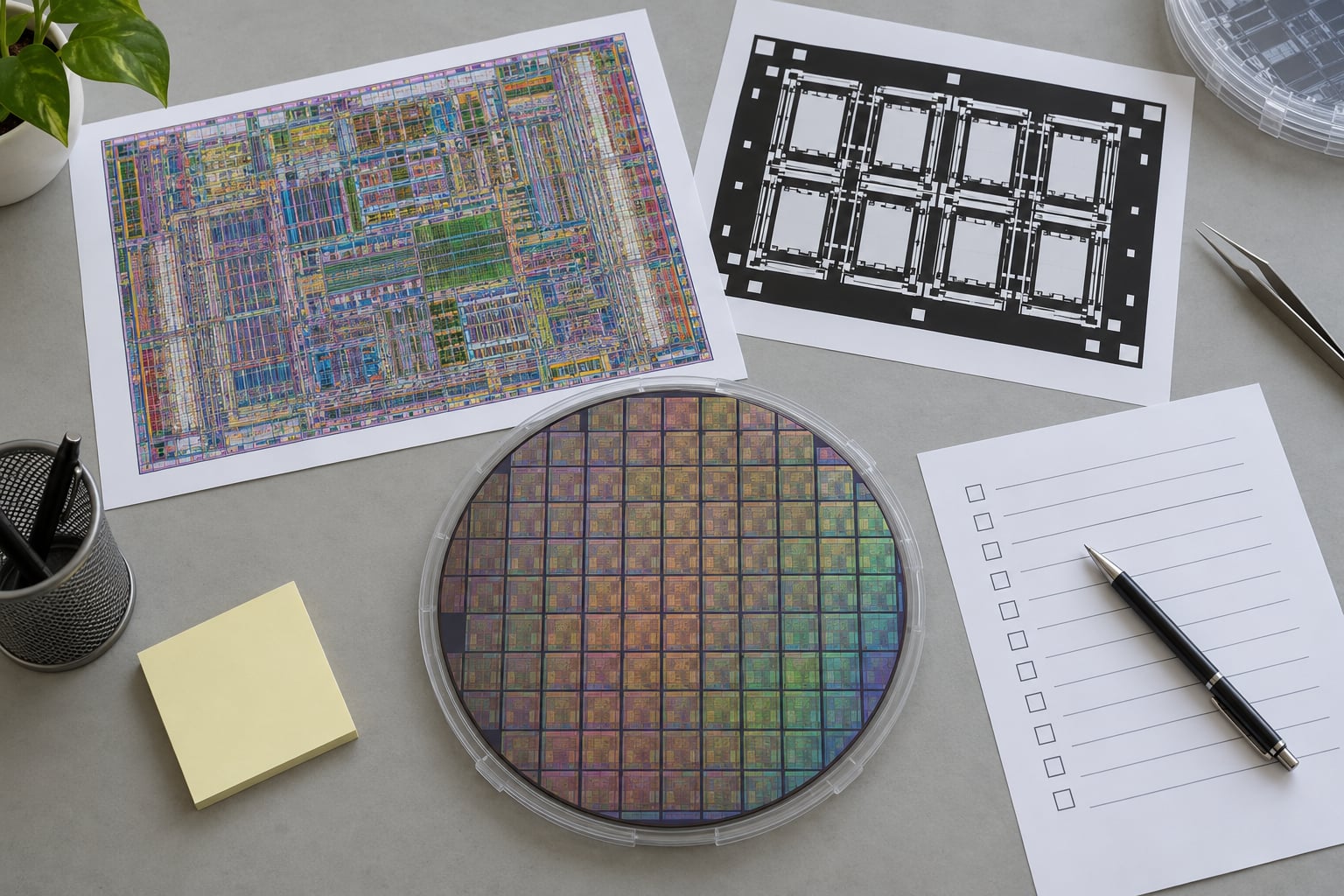
Tapeout is the point in the chip design process at which a fully verified, signed-off layout is formally released to a semiconductor foundry so that photomasks can be fabricated and wafers manufactured. It is a handoff milestone, not the start of production, and everything in the package is translated almost directly into mask data.
Two details hide in that definition. First, “released” is a controlled act: a named release authority signs, the foundry confirms it has received a complete and internally consistent package, and only then does the clock on mask writing start. Second, the physical consequence is permanent for the life of that revision. A shorted net in the layout is not a software bug you can patch. It is a shape that will be patterned onto every die from that mask set.
The word comes from the 1970s, when the artwork was written to magnetic tape and physically shipped to the mask shop. “Tape” no longer describes the medium; it survives in the vocabulary alongside tape-in, which is the mirror-image milestone when a design enters the manufacturing cycle. Industry use of tape-in is inconsistent, so treat it as informal shorthand rather than a formal counterpart.
It is also worth separating the verb from the noun. As a verb, a team tapes out when it releases. As a noun, a tapeout is the release package or the milestone itself. Teams also say “revision one” for the first tapeout of a design, and “respin” for the next one, which is why you will hear tapeout, rev and respin used almost interchangeably in project meetings.
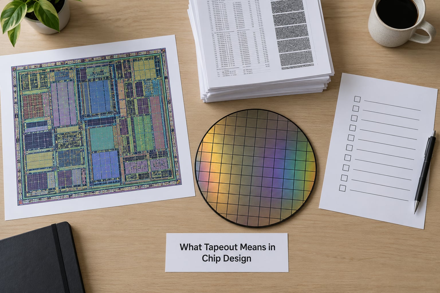
Why it matters comes down to reversibility. Front-end errors are caught in simulation for hours. Back-end errors are caught in days. Post-tapeout errors are caught in months and cost another mask set.
How the Tapeout Process Works
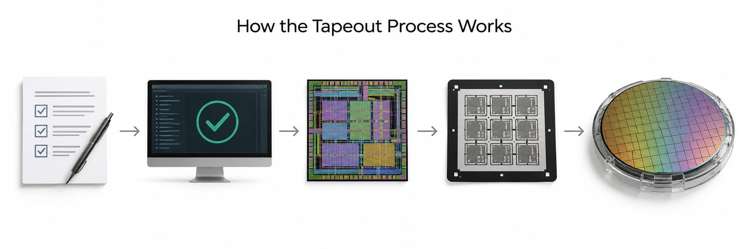
The VLSI design flow that ends at tapeout runs roughly in this order, and each stage hands a specific artifact to the next owner:
- Specification and architecture. Requirements, interface contracts, target process node and packaging assumptions are fixed. Late changes here are the most expensive kind of change.
- RTL design. The design is written and verified against the specification in simulation, usually with UVM-style constrained-random testbenches for complex SoCs.
- Synthesis. RTL is mapped to the target library, producing a gate-level netlist with timing and area estimates.
- Place and route. The netlist is placed on the die and routed, with power planning, clock tree synthesis and signal integrity work happening here.
- Physical verification and signoff. Design rule checking, layout versus schematic, static timing analysis with extracted parasitics, and IR drop plus electromigration analysis all have to close.
- Mask data preparation. Fill is inserted, the padframe and IO definitions are frozen, waivers are documented, and the database is converted to GDSII or OASIS and verified.
- Foundry handoff and wafer fabrication. The foundry accepts the package, a mask set is written, and wafers are processed.
Who owns each stage matters as much as what it produces. On a small team the physical design lead may run signoff personally; on a large program a dedicated tapeout manager or PMO drives the schedule and calls the readiness review.
| Stage | Typical owner | Output at handoff |
|---|---|---|
| Specification and architecture | Systems and architecture lead | Specification, interface contract, node and package decision |
| RTL and verification | Front-end design and DV | Verified RTL, coverage closure report |
| Synthesis | RTL synthesis | Gate-level netlist, area and timing estimates |
| Place and route | Physical design | Routed layout, power grid, clock tree |
| Physical signoff | Physical verification, STA, power integrity | Clean DRC and LVS, timing closure, IR and EM signoff, waiver list |
| Mask data preparation | Layout and physical design | Fill, final padframe, GDSII or OASIS, foundry package |
| Foundry acceptance and fabrication | Tapeout manager and foundry program manager | Accepted package, mask order, wafer schedule |
One practical note on signoff. DRC and LVS are the two checks beginners underestimate most. DRC catches geometry that violates the process rules; LVS confirms that what you built in silicon matches what you drew in the schematic. A design can pass DRC with a perfectly clean layout of a circuit that was never connected the way you intended.
What Is Included in a Tapeout Package?
This is the part most beginner walkthroughs skip, and it is the single most useful thing to know before you start a release. The exact list is set by the foundry’s design manual for the process, but the shape is consistent.
| Deliverable | What it contains | Why the foundry needs it |
|---|---|---|
| GDSII or OASIS layout | The full hierarchical layout database, every metal layer, via, fill and keep-out | The primary manufacturing database; everything else is reference to it |
| Netlist | Gate-level connectivity, either as a Verilog view or in the foundry’s preferred format | Allows the foundry to run connectivity and LVS reference checks |
| SDF or Liberty timing data | Back-annotated parasitic and timing information for the released netlist | Lets the foundry reproduce timing analysis on the final extraction |
| LEF and DEF | Abstract and physical design views for incremental or hierarchical implementation | Required by many foundries for cell-based and larger designs |
| Padframe and IO definitions | Pad locations, names, drive strength, ESD and interface specifications | Defines how the die connects to package and test, and drives pad ring mask layers |
| Fill and density information | Metal fill structures, dummy devices, density distribution targets | Required for planar CMP uniformity and step-height control |
| Waivers and deviation reports | Documented, justified exceptions to design rules with their risk assessment | Foundry approval; unsigned waivers are a release blocker |
| Assembly and test information | Probe card or test program requirements, pad coordinates, package drawing | Where required, so probe and assembly can start the moment wafers finish |
Two lesser-known items are worth calling out. Antenna rules require that a given ratio of gate area to connected metal area be maintained, usually solved with diode insertion or metal jumper devices; skipping them produces reliability failures, not functional ones. Density rules exist because chemical mechanical planarization behaves badly on sparse layouts, so fill is a manufacturing requirement rather than a cosmetic step.
Tapeout vs. Fabrication: Where Does the Boundary Fall?
Most beginner confusion comes from using “tapeout” for several downstream events. The boundary is clear once you name each milestone separately.
| Term | What it means | When it happens |
|---|---|---|
| Tapeout | Design released to the foundry for mask fabrication | Once per revision, at the end of back-end signoff |
| Mask fabrication | Reticle writing and mask inspection from the layout data | Weeks after tapeout, depending on mask set size and set |
| Wafer fabrication | Deposition, lithography, etch and implant across the wafer | Weeks to months depending on node, layer count and foundry load |
| Wafer-out | Wafers leave the process line and move to probe or assembly | After fabrication and before packaging |
| First silicon | The first physical parts you hold, functional or not | After assembly, sometimes before final test release |
| Respin | A corrected design released as a new revision, repeating the whole cycle | When a defect found in silicon must be fixed in layout |
Submitting design data is not receiving silicon. The gap between those two events is measured in months, and it is almost entirely outside your control. What you control is the quality of what you submit, which is why tapeout readiness reviews exist.
How Long Does a Tapeout Take?
There are two separate timelines and people constantly confuse them. The first is the design cycle: spec to tapeout. The second is the manufacturing timeline: tapeout to parts in hand.
Design cycle length is dominated by verification and closure, not by the physical flow. A small block that needs one round of physical convergence can reach signoff in a couple of months; a large SoC with many late requirement changes runs far longer. Public case studies show this is not fixed: ChipFlow reported taping out a RISC-V test chip on a GlobalFoundries 130nm BCD process in under four months, against a typical cycle for that class of chip that often exceeds it.
| Phase | Typical scale | What stretches it |
|---|---|---|
| RTL and verification | Longest phase, often the majority of the cycle | Coverage holes, late spec changes, UVM environment bring-up |
| Synthesis to first routed layout | Days to a few weeks | Timing closure difficulty, congestion, clock tree complexity |
| Physical signoff convergence | Weeks, occasionally months | DRC and LVS violations, IR and EM failures, antenna and density fixes |
| Mask data prep and foundry review | One to three weeks | Waiver negotiation, incomplete package, foundry queue |
| Mask fabrication and wafer processing | Months | Process node, layer count, mask set size, foundry load |
| Assembly and test | Weeks | Package availability, probe card lead time, test program debug |
The variables that actually move the manufacturing side are process node, mask set count, die area and where the foundry’s queue sits that month. Advanced nodes push mask writing and processing time up sharply. You cannot buy your way past the queue, which is why experienced teams lock the design, not just the schedule.
How Much Does a Tapeout Cost?
Tapeout cost is dominated by mask set cost for a given die area, and mask cost scales steeply with process node. The same die costs a small fraction of the money to build on a mature node than on a leading-edge one, which is why almost every analog and mixed-signal part in production today sits on older technology.
The main cost drivers are: the process node and its mask set cost; the number of mask levels, which grows with metal layers and 3D structures; die area, since mask cost scales with it; expected wafer volume, where a small-volume part on an expensive node can be uneconomic; packaging and test; engineering wafers and characterization before volume; and the cost of revisions, since a respin means paying for a second mask set.
| Route | Minimum volume | Main cost driver | Time to silicon | Best for |
|---|---|---|---|---|
| Full mask (dedicated) | Full production volume | Entire mask set paid alone | Longest | Commercial ASICs and SoCs shipping in volume |
| MPW / shuttle run | Tens to thousands of dies | Your share of a shared mask set | Medium, tied to shuttle cadence | Fabless startups and prototyping |
| Foundry-run test chip | One die | Process access and engineering time | Short | Teaching, PDK and characterization work |
| Educational shuttle | One small die | Low fixed program cost, open tooling | Fixed cadence, months of waiting | Students, clubs and hobbyists |
Quoted NRE varies by foundry, technology and project scope, so treat any single figure as a starting point for a conversation rather than a tariff. The structural question is simpler: if your expected lifetime volume cannot justify a full mask set, an MPW or shuttle route spreads that fixed cost across many designs.
The limitation practitioners mention most often is that sharing cost does not make it cheap. As one long-running discussion in r/chipdesign puts it, even after splitting a run the share is still far out of reach for an individual hobbyist, and shuttle slots are oversubscribed. Educational shuttles have partly solved that by publishing fixed per-run pricing, which is why Tiny Tapeout-style programmes have become the standard entry point for students and clubs.
What Happens After a Successful Tapeout?
Once the package is accepted, the design belongs to the process line. Mask writing starts, reticles are inspected, and wafers are processed through deposition, lithography, etch and implant. Assembly is often queued in parallel so wafers can move straight to package when they finish.
What comes back is not guaranteed working silicon. First silicon means the first physical parts, and treating that as a promise of functionality is a common and expensive assumption. Bring-up starts with wafer probe and parametric measurement to confirm the process behaved, then electrical characterization of key circuits.
When something is wrong, failure analysis is the next step: decap, cross-section, and locate whether the fault is in the process, the design, or the test setup. Layout defects get fixed and released as a respin; process-only issues get worked with the foundry; test-only issues get fixed in the test program with no new mask set at all. A good test plan, written before tapeout, is what keeps that last category large.
Common Tapeout Mistakes and How to Avoid Them
Most respins trace back to something that was known, suspected, or simply not checked. The recurring ones:
- Signing off on a waiver nobody approved. A DRC exception with a plausible justification is not signed off until the foundry accepts it in writing. Do the waiver paperwork during signoff, not after the first mask arrives.
- Running the wrong design rule deck. Using a PDK version one release behind the mask set it targets produces violations that either fail review or force late waivers. Pin the deck version in your tapeout checklist.
- Missing a power or ground connection. LVS catches connectivity mismatches, but a single unconnected domain can still slip through as a core-level issue. Check power domain completeness against the padframe intent explicitly.
- Skipping fill or density insertion. This is a process reliability problem that shows up as yield loss, not as a dead chip, which makes it hard to trace back. Make fill a checked deliverable with its own signoff.
- Ignoring antenna rules. Antenna violations cause oxide damage that shows up as a parametric degradation in the field. Fix them with diodes or jumpers at the schematic stage, not at tapeout.
- Leaving packaging until after the handoff. Bond pad arrangement, die edge clearance and thermal constraints affect layout. Deciding the package late can force a respin purely for mechanical reasons.
- Under-planning test. Without a test plan, probe access and test coverage suffer and real defects get mistaken for process variation. Write the test program alongside the padframe.
- Freezing the design without a change-control plan. Post-tapeout ECOs have to be either impossible or explicit. Decide in advance which changes are allowed and what triggers a respin.
A tapeout readiness review exists to catch exactly this list. It is a scheduled meeting with a hard gate, run by the tapeout manager with signoff from design, physical verification, power integrity and whoever owns packaging and test.
Frequently Asked Questions
What is the difference between tapeout and fabrication?
Tapeout is the release of a verified, signed-off design to the foundry. Fabrication is everything the foundry does afterwards: writing the photomasks from your layout data, then processing wafers through deposition, lithography, etch and implant. Submitting the package is a data event you control; fabrication is a manufacturing event with a schedule you do not.
Is tapeout the same as mass production?
No. Tapeout happens once per design revision and starts manufacturing of the first wafers. Those wafers are often engineering samples used for characterization, and they are frequently the only wafers produced for a low-volume part. Volume production comes later, and may never come, if the part is a prototype or a teaching chip.
What files are sent to the foundry for a tapeout?
The core deliverable is the GDSII or OASIS layout database. Alongside it a foundry typically expects the gate-level netlist, back-annotated timing data in SDF or Liberty form, LEF and DEF where the process requires them, padframe and IO definitions, fill and density information, documented design rule waivers, and assembly and test data.
How many tapeouts does a chip usually need?
A well-prepared design can pass with one, but many first chips need a respin to fix yield, timing or functional issues found on silicon. Analog and mixed-signal parts typically need more revisions than digital designs because they are harder to verify before fabrication. Treat the second revision as a scheduled budget item rather than a surprise.
What should a chip designer check before tapeout?
Verify that DRC, LVS, static timing analysis with extracted parasitics, and IR drop plus electromigration analysis have all closed against the correct design rule deck. Confirm fill is inserted, the padframe is frozen, antenna rules are satisfied, every waiver is documented and foundry-approved, and the GDSII was re-verified after conversion. Then hold the readiness review.
Does tapeout include packaging and final testing?
Not the physical work, though the data comes with the package. Packaging happens after wafer-out and final test happens after assembly, usually through an assembly and test supplier. What you do submit at tapeout is the information they need to start immediately, such as pad coordinates, probe requirements and package drawings, so the two schedules overlap.
Conclusion
Tapeout is the release of a verified design to a foundry for mask fabrication, and the reason it carries so much weight is that it is the last moment every error is still free to fix. Everything before it is a simulation; everything after it is metal.
The first action is unglamorous: before assembling the package, confirm that signoff is complete against the correct design rule deck, that the deliverables your foundry’s design manual requires are present and re-verified, that every waiver is documented and approved, and that packaging and test assumptions are settled. Hold a readiness review with a real gate. If that meeting is uncomfortable, the mask set will be worse.