A bandgap reference circuit is an integrated voltage reference that produces an almost constant output, typically about 1.2 V, by adding a voltage that falls with temperature to a voltage that rises with temperature so their slopes cancel. The result barely moves with supply voltage, load, process variation or time, which is why nearly every analog and mixed-signal IC carries one.
- Typical output: 1.2 V, with a workable range of roughly 1.0 V to 1.3 V before scaling
- Initial accuracy: 0.5% to 1.0% untrimmed on a discrete build, far better with wafer-level trim
- Temperature coefficient: 25 to 50 ppm/degC typical, 1.5 to 2 ppm/degC in precision parts
- The name: it comes from the silicon bandgap energy, which is about 1.2 V when the VBE curve is extrapolated to absolute zero
Table of Contents
- What Is a Bandgap Reference Circuit?
- Why Bandgap References Are Stable
- How a Bandgap Reference Circuit Works
- What Is the Bandgap Voltage Equation?
- Which Bandgap Circuit Architectures Are Common?
- Self-Biased Versus Startup-Assisted Bandgap Reference Circuits
- What Design Parameters Control Bandgap Performance?
- How Do Mismatch, Process, Voltage, and Temperature Affect the Output?
- What Is the Role of Curvature Correction?
- How Do You Design One for an IC?
- Where Are Bandgap References Used?
- Frequently Asked Questions
- Why is the bandgap voltage near 1.2 V?
- Is a higher bandgap reference voltage always more accurate?
- What is the minimum current a bandgap reference needs?
- Can a bandgap reference work without a startup circuit?
- How is a 1.2 V reference different from a normal voltage regulator?
- Conclusion
What Is a Bandgap Reference Circuit?

A bandgap reference circuit is a self-contained block that generates a DC voltage referenced to the semiconductor material rather than to the supply rail, the load, or the clock. Designers use it wherever a measurement or a control loop needs a number it can trust: ADC scales, LDO feedback, comparator thresholds, current-mirror bias, PLL charge pumps.
The reason it is needed at all comes from what the alternatives do. A supply rail moves. A Zener diode drifts with current, temperature and aging, and it needs a bias current to stay in its knee. A simple resistor divider is a ratio of two resistors, so it inherits every mismatch between them and every temperature coefficient difference between the films. None of those give you a number that survives a wafer.
The bandgap gets its stability from a property of the silicon itself. The base-emitter voltage of a bipolar transistor falls predictably as temperature rises, while the difference in base-emitter voltage between two transistors running at a fixed current density ratio rises with temperature. Those two slopes are related to the same bandgap energy, so you can scale one until it exactly cancels the other.
Three terminals is the normal interface: supply, ground, and output. Supply and ground may swing widely, and the output barely notices. That decoupling between the output and everything around it is the whole point, and it is why the bandgap is usually the last block checked when an LDO’s PSRR looks worse than the datasheet claims.
Why Bandgap References Are Stable
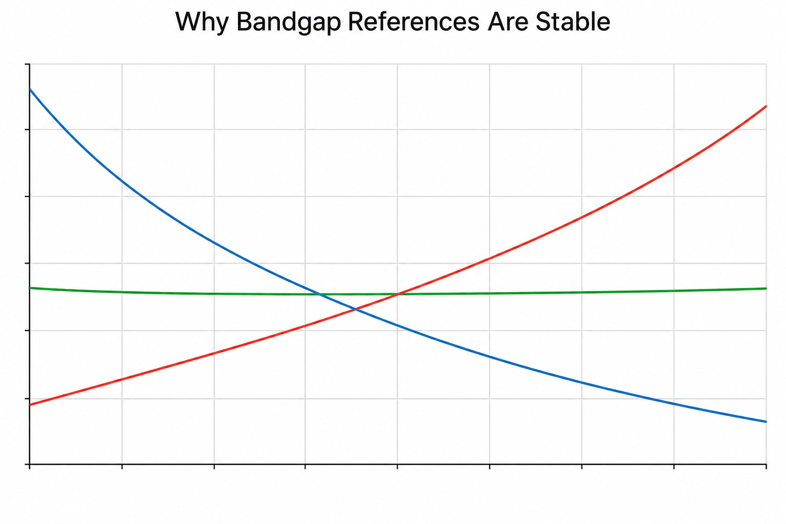
The stability comes from cancelling two temperature effects that move in opposite directions. A base-emitter voltage (VBE) is CTAT, complementary to absolute temperature, falling by roughly 2 mV per degree Celsius at constant collector current. A delta-VBE between two area-mismatched transistors is PTAT, proportional to absolute temperature, rising with the thermal voltage VT = kT/q.
The first expression everyone learns is the diode equation, VBE = VT ln(Ic/Is), where Is is the saturation current and VT = kT/q. At room temperature VT is about 25.85 mV, and that factor of T is what makes VBE fall as temperature climbs.
Now bias two transistors at the same collector current but with different emitter areas, one of them N times larger than the other. The same current through a bigger junction gives a smaller current density, so the larger device sits at a higher VBE. The difference between the two base-emitter voltages is VBE = VT ln(N), and because it inherits VT with the natural logarithm of the area ratio baked in, it rises linearly with absolute temperature.
So you have one quantity falling at about 2 mV per degree and another rising at a slope you can set by choosing N. The rising term goes through a resistor to develop a voltage, and a scaling factor M is chosen so that M times the PTAT voltage equals the magnitude of the CTAT slope. Add them and the first-order temperature term vanishes.
| Term | Symbol | Behavior vs temperature | How it is produced |
|---|---|---|---|
| Base-emitter voltage | VBE | Falls about 2 mV/degC (CTAT) | Diode-connected bipolar transistor at constant current |
| Thermal voltage | VT = kT/q | Rises 86.17 uV/degC (PTAT) | Set by the Boltzmann constant and electron charge |
| Difference in VBE | dVBE = VT ln(N) | Rises linearly with T (PTAT) | Two transistors, emitter area ratio N, equal current |
| Sum | VBG = VBE + M dVBE | Nearly flat when M is chosen correctly | Resistor-weighted summing at the output |
How a Bandgap Reference Circuit Works
Every practical bandgap follows the same signal chain, whether it is a three-transistor Brokaw loop or something far more elaborate. Matched bias currents feed the area-mismatched transistor pair. The delta-VBE between that pair is amplified by a resistor ratio, summed with a CTAT VBE, and the result is buffered to the output.
Three functions sit behind that description. The VT generator is the mismatched pair plus its current mirror; it makes the PTAT term. The amplifier or scale factor is the resistor network that turns the small dVBE into something like 10 to 30 times VT. The summing stage adds that to the CTAT voltage and often buffers it so the output can drive a load without dragging the loop around.
Two closed-loop structures are worth knowing. In a current-mode design such as Brokaw, the amplifier forces the voltages at two nodes equal, and the resistor ratio sets how much current flows through the PTAT leg; the total current is the output. In a voltage-mode design, the amplifier drives a resistive divider and the loop settles when the divider output equals the CTAT node.
Device matching matters more here than in most analog blocks, and the reason is specific. The cancellation only works if both terms are computed at the same temperature and the same current density. Mismatch between the mismatched transistors changes the effective area ratio N, which moves the PTAT slope, which shifts the trim point along the drift curve. On chip designers fix this with common-centroid or cross-quadrilateral layout of the transistor pair and with large-area, lightly loaded resistors.
On r/chipdesign this is the point that catches people out most often. Changing a resistor value in simulation moves the curvature of the drift curve far more than most designers expect, because that resistor sets the scale factor and therefore the balance point between the PTAT and CTAT slopes.
What Is the Bandgap Voltage Equation?
The bandgap reference voltage is the CTAT base-emitter voltage plus a scaled PTAT term: VBG = VBE + M times VT ln(N), where M is the scale factor set by the resistor ratio and N is the emitter area ratio. When M is chosen so that the two slopes cancel, VBG holds nearly constant.
Deriving the name shows where 1.2 V comes from. Linearize the VBE curve to absolute zero and you get the silicon bandgap voltage, roughly 1.205 V, plus a temperature-independent term written as a multiple of the R0 resistance ratio. With the usual values for silicon and germanium junction work functions, the classic result lands around 1.2882 V at 300 K. Both figures are correct for different assumptions about the work functions, which is why datasheets say 1.2 V.
A worked example makes the cancellation concrete. Take an emitter area ratio of N = 8. Then dVBE = VT ln(8), which is about 2.08 VT. Choose the resistor ratio so that the PTAT leg develops 11 times that dVBE, giving a PTAT contribution of about 22.9 VT. At 300 K, 22.9 VT is roughly 592 mV.
Add a VBE of about 656 mV at the same bias current and the sum is approximately 1.248 V. That is a perfectly ordinary bandgap output, and the 2 mV per degree slope of the VBE is now cancelled by the 22.9 VT term rising at the right rate. The two numbers are not independent, which is why you solve the resistor sizing iteratively rather than picking values by hand and hoping.
Which Bandgap Circuit Architectures Are Common?
The common architectures differ mainly in how they bias themselves, how they improve output impedance, and whether they correct curvature. Self-biased and startup-assisted loops are the base case. Brokaw and Banba are the two classic named topologies. Cascode and curvature-corrected variants are the precision options.
| Architecture | Output | Minimum supply | Strength | Tradeoff |
|---|---|---|---|---|
| Self-biased (Widlar-style) | About 1.2 V | Around 1.4 V | Fewest devices, smallest area | Must be forced out of the zero-current state |
| Startup-assisted self-biased | About 1.2 V | Around 1.4 V | Reliable power-up, still compact | Startup current adds to total supply current |
| Brokaw | About 1.2 V, current output | Around 1.4 V | Compact loop, well understood, easy to trim | Simple amplifier, modest PSRR |
| Banba (current-summed) | About 1.2 V | Around 1.2 to 1.4 V | Runs from lower supply, CMOS-friendly | Needs resistive averaging, poorer matching |
| Cascode | About 1.2 V | Higher | Much better line regulation | Voltage headroom, area, capacitance |
| Curvature-corrected | About 1.2 V | 1.4 V and up | Flattens the bow-shaped drift | Extra devices, trim, or calibration logic |
The Banba topology deserves a note because it is the usual answer for a sub-1 V supply. Instead of summing voltages, it sums currents: two currents proportional to the CTAT and PTAT voltages flow into a resistor, and the voltage across it is the reference. The catch is that those currents must come from resistors that actually match, and resistor mismatch enters the output directly.
Below about 1.2 V of supply, a classic voltage-summed bandgap simply has no headroom, because the output alone needs more than the rail. The fixes are current-summed cores, sub-1 V VBE references stacked differently, or fractional bandgaps where the same cancellation is scaled down to a fraction of a volt.
Self-Biased Versus Startup-Assisted Bandgap Reference Circuits
A self-biased bandgap has exactly one stable operating point and a second one at zero. With no current anywhere, every transistor sits at zero VBE, the amplifier sees a balanced input, and nothing pushes the loop out of that state. The circuit is perfectly stable at zero forever. This is the single most repeated question on chip design forums, and the answer is always the same: nothing in a self-biased loop can start itself.
A startup circuit fixes it. The usual form is a current source or a biased transistor that steals a few microamps from the supply and injects it into the feedback node until the main loop begins conducting. Once the loop is up, the startup device is biased off, usually by the rising voltage at the very node it was feeding, so it stops contributing.
The design tension is that the startup current must be large enough to escape the zero state on the slowest, lowest-supply, highest-temperature corner, and small enough that it does not wreck the power budget or push the loop into a state where both devices conduct at once. Engineers usually sweep it across all corners in transient simulation with the main loop’s own settling time as the pass criterion.
The alternative is to remove the ambiguity. Biasing the reference from a supply-independent current source or from an already-biased block gives the loop a defined starting current, at the cost of coupling and of a dependency on another block being functional. For a reference that must come up first in the chip, the startup-assisted self-biased loop is usually the practical answer.
What Design Parameters Control Bandgap Performance?
Each performance number a designer cares about traces back to a specific parameter in the circuit. Temperature coefficient comes from the scale factor M and from any uncorrected curvature. Initial accuracy comes from resistor ratios, VBE at the chosen bias current, and how much of it gets trimmed away. Line and load regulation come from the output impedance of the buffer and from supply rejection inside the loop.
Current consumption is set by the PTAT leg current and the branch current of every device in the loop. Noise is dominated by flicker noise from the input devices and by resistor excess noise, and it is why chopping or averaging techniques appear in precision parts. Die area is driven by resistor values, which in turn are driven by how much current you can afford to push through them.
Startup margin is its own design target rather than a by-product. It is the difference between the worst-case startup current and the current needed to reach the operating point, and a reference that is marginal at the cold, low-supply corner will pass a bench test in August and fail qualification in January.
Two figures frame the realistic range. Uncompensated discrete and simple integrated references land around 25 to 50 ppm/degC. Curvature-corrected integrated parts reach 1.5 to 2 ppm/degC, and that gap is bought with area, power and calibration effort rather than with a cleverer equation.
Noise sits in the 0.6 to 2 uV per square root Hz range for typical parts, which is low but not negligible when you feed it into a high-resolution converter. Supply rejection of 60 to 100 dB at low frequencies is typical, falling off as the loop stops following the rail at higher frequency.
How Do Mismatch, Process, Voltage, and Temperature Affect the Output?
Once you know the ideal equation, the useful part is knowing which non-ideal effect dominates which error term. The table below is the version I keep next to a design review: symptom, likely cause, main mitigation.
| Error source | What it looks like | Likely cause | Main mitigation |
|---|---|---|---|
| Residual temperature drift | Bow-shaped curve peaking at a mid temperature | Uncorrected curvature in VBE, wrong scale factor | Curvature correction, careful M selection, wafer trim |
| Initial accuracy error | Output sits high or low at 25 degC | Resistor ratio tolerance, VBE process spread, bias current error | Matching layout, trimming, calibration in test |
| Supply sensitivity | Output moves when the rail moves | Limited loop gain, finite output impedance of the buffer | Cascade, cascode, or a buffered second stage |
| Load regulation | Output droops into a heavy load | Non-ideal output buffer, output impedance | Push-pull buffer, unity-gain buffer stage |
| Emitter area mismatch | Drift curve peak shifts in temperature | Poor cross-matching of the mismatched transistor pair | Common-centroid layout, large emitters, moderate N |
| Bias current error | Output and temperature coefficient both shift | Reference current source mismatch | Trimming or a self-referenced current mirror loop |
Simulation-to-silicon mismatch is the recurring frustration in forum threads about this block. A schematic that shows a flat drift curve tells you very little, because the layout decides the matching and the trim decides the rest. The honest framing is that no real circuit reaches exactly zero temperature coefficient. The real question is how close you need, and for most silicon that lands in the tens of ppm per degree.
Process corners matter in a specific order. VBE varies with the saturation current Is, which moves the CTAT term and shifts the trim temperature. Resistor sheet resistance varies, which changes the gain of the PTAT leg. MOS threshold and mobility variation matter for the startup device and the amplifier, and matter much less for the core, which is why bipolar or thick-oxide devices are still preferred in the core where the process allows it.
What Is the Role of Curvature Correction?
The bandgap cancels the linear part of VBE’s temperature dependence, which leaves a second-order, parabolic residual. That is why a basic reference has a bow-shaped drift curve whose worst error is not at the temperature extremes but somewhere in the middle of the range, usually between 20 and 50 degC. Quoting a single ppm per degree figure without saying where it was measured hides exactly this problem.
Curvature correction reshapes the residual. The simplest version splits the CTAT contribution across several diode-connected devices biased at different current densities, each contributing a different amount of curvature, and sums them with the right weights. Piecewise schemes switch between curvature-corrected segments as temperature crosses a threshold. Digital schemes store a lookup of the error and correct it in the output path, which is common when a microcontroller already has the calibration memory available.
Malcovati’s 2001 work on a 1.2 V reference with sub-ppm per degree performance is the reference most designers point to for the analog approach, and later work pushed the idea further with current-mode corrections. The trade is always the same: each correction adds devices, adds a trim, and moves error from temperature into initial accuracy, where calibration can reach it.
One forum observation worth repeating: changing a resistor in a literature-sourced design moves the amplitude of the bow but does not by itself shift where the bow peaks. Shifting the peak in temperature means changing the balance between the CTAT and PTAT contributions, not just their overall gain. That is a small distinction that costs a lot of simulation time if nobody points it out.
How Do You Design One for an IC?
Design a bandgap by fixing four things first: target output voltage, temperature range, accuracy requirement, and current budget. Everything downstream is arithmetic once those are set. If the output has to be 2.5 V, you scale the 1.2 V core by a resistor divider or a gain stage, and the divider’s own temperature coefficient enters the error budget.
Then pick the topology. Above a 1.4 V supply, a self-biased or startup-assisted Brokaw-style loop is the usual starting point because it is compact and well characterised. For a lower supply, go current-summed. For tight temperature stability, plan curvature correction from the start rather than adding it later, because the correction network needs its own trim.
Next size the devices. Pick the PTAT leg current first; higher current improves matching and reduces the relative effect of resistor noise but costs power and area. Then pick the emitter area ratio N. Small N keeps the devices small but reduces the signal, which hurts temperature coefficient after trimming. Values between 4 and 8 are a common compromise in integrated designs.
Now solve the resistors so you hit the target voltage and zero temperature coefficient at the same time. Write the output equation with your chosen VBE, dVBE = VT ln(N), and resistor network, then adjust the scale factor to null the slope and the output ratio to set the DC level. Do it iteratively in simulation, not on paper, because VBE depends on the bias current you just chose.
Verify in this order: a temperature sweep with the supply fixed, then a supply sweep at the temperature corners, then Monte Carlo with layout-extracted mismatch, then PSRR and noise, then a transient power-up run with the slowest corner and a low supply. Layout is not a later step here. Cross-quadrilateral layout for the mismatched pair, guard rings around the PTAT branch, and thermal symmetry between the pair and the CTAT device decide whether the silicon matches the simulation.
Finally, plan the trim. Most production references are wafer-level trimmed to a target value, and that trim exists to remove the initial accuracy error, not the temperature error. Keeping those two separate in your error budget stops you from trimming the wrong thing.
Where Are Bandgap References Used?
Bandgap references are used wherever a circuit needs a voltage it can trust more than the supply rail gives it. The list is short enough to memorise and long enough to matter.
- ADC and DAC scaling: a drifting reference scales every code in the converter, so reference noise appears directly as input-referred noise
- LDO control loops: the error amplifier compares against the bandgap, which sets the output accuracy and the loop’s PSRR floor
- Comparators and thresholds: a bandgap gives a rail-independent trip point for battery monitoring
- Current sources and bias generators: a Brokaw-style current output feeds precision mirrors
- Mixed-signal microcontrollers: an internal bandgap serves the ADC, comparators and often a temperature sensor on the same die
- Linear regulators: the classic 78xx and 79xx families, and adjustable parts such as the TL431, are bandgap references with a pass transistor attached
- Temperature sensing: run the reference as a constant current and the output voltage tracks temperature directly, which is the basis of silicon bandgap temperature sensors
Where a bandgap is overkill, a simpler reference wins. If the only job is to give a resistor divider a ratiometric node, a divider is cheaper and quieter. If the requirement is long-term stability over years rather than millivolt accuracy, a Zener or a buried Zener reference beats a bandgap. If the part must run from a 600 mV rail, a back-to-back diode stack or a CMOS-only structure may be the only thing that fits.
Frequently Asked Questions
Why is the bandgap voltage near 1.2 V?
Because it is built from two terms that share one physical origin. The CTAT base-emitter voltage extrapolates to the silicon bandgap energy, about 1.205 V, as temperature goes to absolute zero. Adding a PTAT term tuned to cancel the slope lands the room-temperature output near 1.2 V, or 1.2882 V when the junction work-function terms are included. Datasheets say 1.2 V because that is the practical round number.
Is a higher bandgap reference voltage always more accurate?
No. Output voltage is set by the resistor ratio and the CTAT node, not by the cancellation itself. A 2.5 V reference built by scaling a 1.2 V core is usually less accurate than the core, because the divider resistors add their own tolerance and temperature coefficient to the error budget. Choosing a higher output to gain headroom or dynamic range is reasonable; assuming it buys accuracy is not.
What is the minimum current a bandgap reference needs?
There is no universal number, because the branch current is a design choice that trades matching and noise against power. Typical integrated references run the PTAT leg somewhere between a few microamps and a few hundred microamps, with total supply current often quoted in the tens to hundreds of microamps. Larger currents improve matching and reduce resistor noise. Verify the minimum on the cold, low-supply corner rather than at room temperature.
Can a bandgap reference work without a startup circuit?
Only if something else starts it. A self-biased loop has two stable states: the correct operating point, and zero current everywhere, where it is perfectly happy to sit forever. Biasing the reference from an already-running current source, or from another functional block, does start it, at the cost of coupling and sequencing. Most designs that must come up first on the die use an explicit startup circuit that switches itself off once the loop is running.
How is a 1.2 V reference different from a normal voltage regulator?
A regulator takes an input voltage and holds an output voltage. A reference does not regulate at all: it defines a level that stays put while the supply moves, the load changes, and temperature varies. Its accuracy comes from the cancellation of two temperature-dependent effects in silicon, not from feedback on an error signal. Regulators such as the LM317, the TL431 and the 78xx families are built around a bandgap reference plus a pass stage.
Conclusion
A bandgap reference works because two silicon effects that move in opposite directions with temperature are scaled until their slopes cancel, leaving a voltage tied to the material’s bandgap energy rather than to the supply rail. That is the whole mechanism, and every topology, trim and curvature scheme is a variation on it.
Start by fixing four numbers before drawing anything: target output voltage, temperature range, required accuracy, and current budget. Those four decide the topology, the minimum supply, and whether curvature correction belongs in the first revision. As 2026 keeps pushing mixed-signal integration toward lower supplies, current-summed and sub-1 V cores are worth understanding before you need them.