The FPGA design flow for beginners is the same sequence every engineer follows: define the spec, write RTL, simulate it, synthesize it, add constraints, place and route, generate a bitstream, and bring the board up. The stages never change, only the menu names do. On a good board, a blinking LED goes from empty project to running in under an hour of tool time. The slow part is learning to read the reports each stage hands you, and that is where beginners usually get stuck.
This guide walks the whole flow end to end, using a 4-bit counter that lights LEDs on a Digilent Basys 3 as the running example. It is deliberately tool-light on menus and heavy on the files and reports you will actually meet, because those are the parts that transfer when you change vendors or board.
If you are coming from embedded C, one warning up front. RTL is not software. There is no while loop that runs until something is true, no function call stack, and a bug in a clocked block does not crash, it quietly produces wrong bits on real hardware forever.
Table of Contents
- What You Need Before Starting
- Step-by-Step: The FPGA Design Flow for Beginners
- Step 1: Define the Requirements and Architecture
- Step 2: Create the Project and Set the Constraints
- Step 3: Write RTL Modules in HDL
- Step 4: Run Functional Simulation
- Step 5: Run Synthesis and Review the Reports
- Step 6: Implement the Design and Place-and-Route It
- Step 7: Analyze Timing and Fix Problems
- Step 8: Generate the Bitstream and Program the FPGA
- Step 9: Validate on Hardware and Iterate
- Common Mistakes in the FPGA Design Flow
- Frequently Asked Questions
- What is the FPGA design flow?
- What is the first step in FPGA design?
- What is the difference between synthesis and implementation in FPGA?
- What is a bitstream file in FPGA?
- Which HDL should I learn first: Verilog or VHDL?
- What is an FPGA constraint file (XDC, UCF, QSF)?
- Do I need a development board to learn FPGA?
- Conclusion
What You Need Before Starting
You need four things: a board, a programming cable, a toolchain, and a small amount of digital logic knowledge. That is genuinely it. Everything else in this article is built on those four.
A development board. Any board with an FPGA and a USB or JTAG programming interface will do. The Digilent Basys 3 and Nexys boards, the Digilent Arty, the Terasic DE0 series, and the Lattice iCEstick are all common starting points. A board with a handful of LEDs, switches, buttons and a 100 MHz oscillator is more than enough to learn the flow. The board’s clock frequency matters because it becomes your timing target, not because a faster clock teaches you more.
The programming cable. Usually a USB cable supplied with the board. A few boards use a separate JTAG or micro-JTAG cable, and a handful use an SD card slot instead of a direct programming port. Check what your board ships with before you start downloading multi-gigabyte tools.
An installed toolchain. The three mainstream vendor tools are AMD/Xilinx Vivado, Intel/Altera Quartus Prime, and Lattice Diamond with Radiant. All three have free editions that cover small to medium devices, and Vivado and Quartus both have separate free licenses for students and hobbyists. There is also an open-source route using Yosys for synthesis and nextpnr for place and route, which works well for small designs and is worth learning later, not first.
Tools, at a glance:
| Tool | Vendor | Typical use | Entry style |
|---|---|---|---|
| Vivado | AMD (formerly Xilinx) | Basys 3, Arty, Nexys, Artix-7 and up | HDL or block design |
| Quartus Prime | Intel (formerly Altera) | DE-series boards, Cyclone devices | HDL or block design |
| Diamond / Radiant | Lattice | Certus and iCE40 / iCE40UP devices | HDL or block design |
| Yosys + nextpnr | Open source | Learning, iCE40, small open designs | HDL, command line |
Two things to keep separate in your head. The design flow itself is vendor-independent, and the tools are just implementations of it. When you see a tutorial that says Run Synthesis and a manual that says Tools then Run, those are the same stage. Knowing the flow means you can read any vendor’s documentation.
Fundamentals. Binary and hexadecimal arithmetic, basic Boolean algebra, and the idea of a clock and a register. Combinational versus sequential logic, setup and hold time, and a rough sense of propagation delay. This is the single most reported blocker in beginner threads, and it is cheap to close: a few weeks of digital logic coursework, or one solid introductory chapter, will save you weeks of confused debugging later.
Reference material you will keep open. The board user manual with its pin table, the FPGA family datasheet or the device’s Resource and Pinout report, and the tool’s user guide. The pin table is where every pin number in your constraint file comes from, so treat it as required reading, not optional.
Step-by-Step: The FPGA Design Flow for Beginners
Here is the whole flow in one list, then each stage in detail.
- Define requirements and architecture. Clock, reset, interfaces, resources, and how you will prove it works.
- Create the project and set constraints. Pick the exact device, package and speed grade, then describe pins and clock timing.
- Write RTL modules. Synthesizable Verilog or SystemVerilog with clean clock and reset structure.
- Simulate functionally. Build a testbench, run it, inspect the waveform, fix everything.
- Synthesize. Convert RTL into a mapped netlist and read the utilization and warning reports.
- Implement. Optimize, place and route the design onto the physical device.
- Analyze timing. Check setup and hold slack, find the critical path, fix and re-run.
- Generate the bitstream and program. Produce the configuration file and load it over JTAG.
- Validate on hardware and iterate. Bring up in a known order, compare against simulation, document, improve.
Step 1: Define the Requirements and Architecture
You turn a vague idea into a testable specification before you write a line of HDL. For a counter on four LEDs the spec is short: a 100 MHz single-ended clock, one active-low reset button, four active-high outputs, count 0 to 15, wrap to 0. That is enough to design against and, more importantly, enough to write a testbench that proves it.
Six items belong in this spec:
- Clock source, frequency and which pin it enters on
- Reset style: asynchronous active-low, synchronous active-low, or no reset at all
- Every external interface, its direction, width and I/O voltage standard
- Expected resource use if it matters, such as block RAM for a buffer
- Timing target, which is normally just the input clock period
- The pass criteria: what result means the design is done
Draw a block diagram next. One box per module, arrows for data, labelled ports on every arrow. It takes ten minutes and it stops you from writing a 400-line module that turns out to need three.
Step 2: Create the Project and Set the Constraints
Project creation is where you commit to hardware, and the part number is not a detail. A board sold with a specific FPGA has a fixed device, package and speed grade printed in its user manual. Choosing the wrong one gives you a project that compiles and then fails at implementation with a confusing message about the part.
Two constraint files matter for a first project, and they carry different information.
The constraint file (XDC for Vivado, QSF for Quartus, LPF for Lattice) tells the tool which physical pins your logical ports connect to, what I/O standard each pin uses, and what clock frequency the design must meet. The clock line is the one beginners leave out, and it is the reason so many first designs report impossible timing failures.
What a minimal Vivado XDC file looks like for a 4-bit counter on a Basys 3:
set_property -dict { PACKAGE_PIN E3 IOSTANDARD LVCMOS33 } [get_ports clk]
set_property -dict { PACKAGE_PIN C2 IOSTANDARD LVCMOS33 } [get_ports rst]
set_property -dict { PACKAGE_PIN U2 IOSTANDARD LVCMOS33 } [get_ports led[0]]
set_property -dict { PACKAGE_PIN U1 IOSTANDARD LVCMOS33 } [get_ports led[1]]
set_property -dict { PACKAGE_PIN W4 IOSTANDARD LVCMOS33 } [get_ports led[2]]
set_property -dict { PACKAGE_PIN W1 IOSTANDARD LVCMOS33 } [get_ports led[3]]

create_clock -period 10.000 -name sys_clk [get_ports clk]
set_property -dict { ASYNC_REG FALSE } [get_ports rst]
Ten nanoseconds is 100 MHz. Get the pin numbers from the board manual, not from a blog post written for a different board revision, because that mistake produces a design that works on the reviewer’s desk and does nothing on yours.
Step 3: Write RTL Modules in HDL
RTL describes hardware that runs on every clock edge, so only a subset of Verilog or SystemVerilog is synthesizable. No delays, no initial blocks that drive outputs, no dynamic arrays in your design logic, and no while loops with conditions the synthesizer cannot unroll. Testbenches are exempt, because they never go into the fabric.
Conventions worth sticking to from day one: one clock domain per always block, a single well-known reset style across the design, a non-blocking assignment inside sequential logic, and a combinational always block that assigns defaults first and then overrides. Those four habits prevent most beginner bugs.
The counter, in synthesizable SystemVerilog:
module counter #(
  parameter int WIDTH = 4
) (
  input  logic             clk,
  input  logic             rst_n,
  output logic [WIDTH-1:0] led
);

  always_ff @(posedge clk or negedge rst_n) begin
    if (!rst_n) led <= '0;
    else        led <= led + 1'b1;
  end

endmodule
That is the whole design. The asynchronous reset sets the counter to zero when the button pulls rst_n low, and everything else is a register counting up and wrapping at 16.
Which language to start in is a real question, so here is the honest comparison:
| Language | Strengths for beginners | Watch-outs |
|---|---|---|
| Verilog | Smallest surface, most tutorials, most example code online | Weak typing, verbose for complex designs |
| SystemVerilog | Adds logic types, assertions and better testbench tooling | Larger language, more ways to write confusing code |
| VHDL | Strong typing, aerospace and defence standard | More syntax before you see a working circuit |
For a first project, start in Verilog or SystemVerilog with Vivado. The example code you will find online is overwhelmingly in that pair, and Vivado’s testbench and assertion features reward the jump to SystemVerilog once you have the flow working. Move to VHDL later if your course or employer uses it, since the flow does not change at all, only the syntax does.
Step 4: Run Functional Simulation
Simulation proves your logic does what you think it does, and it costs seconds instead of a board bring-up cycle. This is where the FPGA design flow pays for itself, and where beginners most often skip ahead.
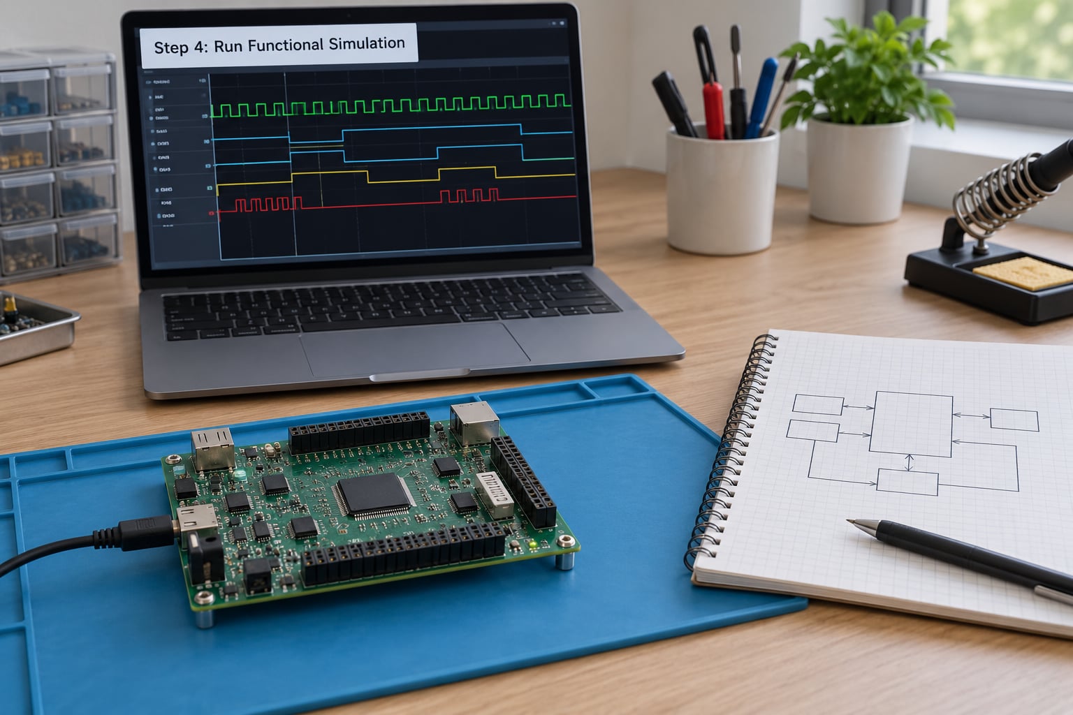
A testbench is a second module that drives your design and checks the answer. It is simulation-only code, so it can use anything the synthesizable subset forbids.
module counter_tb;
  logic       clk = 0;
  logic       rst_n = 0;
  logic [3:0] led;

  counter dut (.clk(clk), .rst_n(rst_n), .led(led));

  always #5 clk = ~clk;   // 100 MHz simulation clock

  initial begin
    $dumpfile("counter.vcd");
    $dumpvars(0, counter_tb);

    #20 rst_n = 1;        // release reset after two cycles

    repeat (40) @(posedge clk);
    $finish;
  end
endmodule
Open the resulting counter.vcd in GTKWave, Simulator or any waveform viewer. What you are looking for is a clean repeating 4-bit count, a known state after reset, and no X values anywhere. An X in a waveform almost always means an uninitialized register, a missing reset, or a signal with no driver.
How do you know it worked? Add assertions or comparison logic so the testbench fails loudly instead of relying on your eyes, and run a few thousand cycles rather than twenty. Simulation speed is the cheapest resource you will ever have.
What you can honestly say after a clean run is that your design is functionally correct for the cases you wrote. It is not proof it will meet timing, fit the device, or survive synthesis, and treating simulation success as design completion is the most expensive mistake in this list.
Step 5: Run Synthesis and Review the Reports
Synthesis translates your RTL into a netlist mapped onto real FPGA primitives: lookup tables for logic, flip-flops for registers, dedicated block RAM for memories and DSP slices for arithmetic. The tool also removes logic it proves is dead and restructures code that maps poorly.
Read two reports and no others on a first project. The utilization summary tells you how many LUTs, registers, block RAMs and DSP slices you used against the device total, and it is your early warning for a design that will not fit. The warnings list tells you what the tool had to work around, such as an inferred latch, a multiply written inefficiently, or a signal that had to be replicated to fix a fanout problem.
Latches are the one warning to treat as an error. A latch in sequential design almost always means a combinational always block with no else branch, so the circuit latches its last value instead of driving a defined one. Fix the code, do not waive the warning.
| Stage | Input | Tool does | Output | Catches |
|---|---|---|---|---|
| Simulation | RTL plus testbench | Computes values cycle by cycle | Waveform and pass or fail | Logic and coding errors |
| Synthesis | RTL plus constraints | Maps to device primitives | Netlist, utilization, warnings | Non-synthesizable code, over-use of resources |
| Implementation | Netlist plus constraints | Places and routes on silicon | Placed routed design, timing report | Timing, pin, routing and DRC failures |
That table answers the difference between synthesis and implementation in one view. Synthesis asks whether the logic can be built. Implementation asks whether it can be built and still run fast enough on this specific device.
Step 6: Implement the Design and Place-and-Route It
Implementation, also called place and route, is where the abstract netlist becomes a physical circuit. The tool picks which logic cells in which I/O sites, connects them with routing resources, inserts the clock network, and then checks the result against the device’s design rule checks.
Place and route is where physical reality intrudes, which is why a design can pass synthesis and fail here. The most common causes:
- Pin assignments that do not exist on your package, or pins that are tied to something else on the board such as a configuration pin
- Drive strength or I/O standard mismatches that violate the bank’s voltage rules
- A design that fits the logic but overruns the available routing
- A clock domain that the tool cannot route to a global clock buffer, causing routing congestion
Check the implementation log first, then the DRC report. If it says a net is unrouted, that is a placement or constraint problem, not a code problem, and reading your RTL again will not help.
Step 7: Analyze Timing and Fix Problems
Timing analysis compares the arrival time of every path against the clock period. Setup slack is the margin on the longest path: positive means it meets the requirement, negative means it is too slow. Hold slack is the minimum margin on the fastest path, and a hold failure is a real hazard rather than a slow-but-working circuit. The worst slack across all paths is reported as WNS, or worst negative slack, and your target is simply to get it positive.
When slack is negative, start from the report, not from your code. It names the critical path: the exact chain of cells from a source register to a destination register, with the logic depth and the delay per cell. Common fixes, roughly in order of how often they work:
- Add a pipeline register along the path, splitting one long combinational chain into two shorter ones
- Remove an unnecessary combinational stage, such as an operator that creates more logic than the surrounding code needs
- Move a multiply or add into a DSP slice instead of building it out of LUTs
- Use a block RAM instead of a large distributed memory built from registers
- Check your clock constraint, because a missing or wrong period produces a failure that is not a design fault
Never fix a timing failure by adding a false path constraint. That silences the report while the real timing problem stays on the board, and it is the shortcut that causes intermittent bugs that nobody can reproduce.
Step 8: Generate the Bitstream and Program the FPGA
The bitstream is the configuration file that tells the FPGA exactly how to wire itself: which LUTs hold which truth table, which flip-flops start where, which routing paths connect them. There is no program to write and no operating system on the device. The FPGA is a blank slate of configurable fabric that becomes your circuit only while the configuration is loaded.
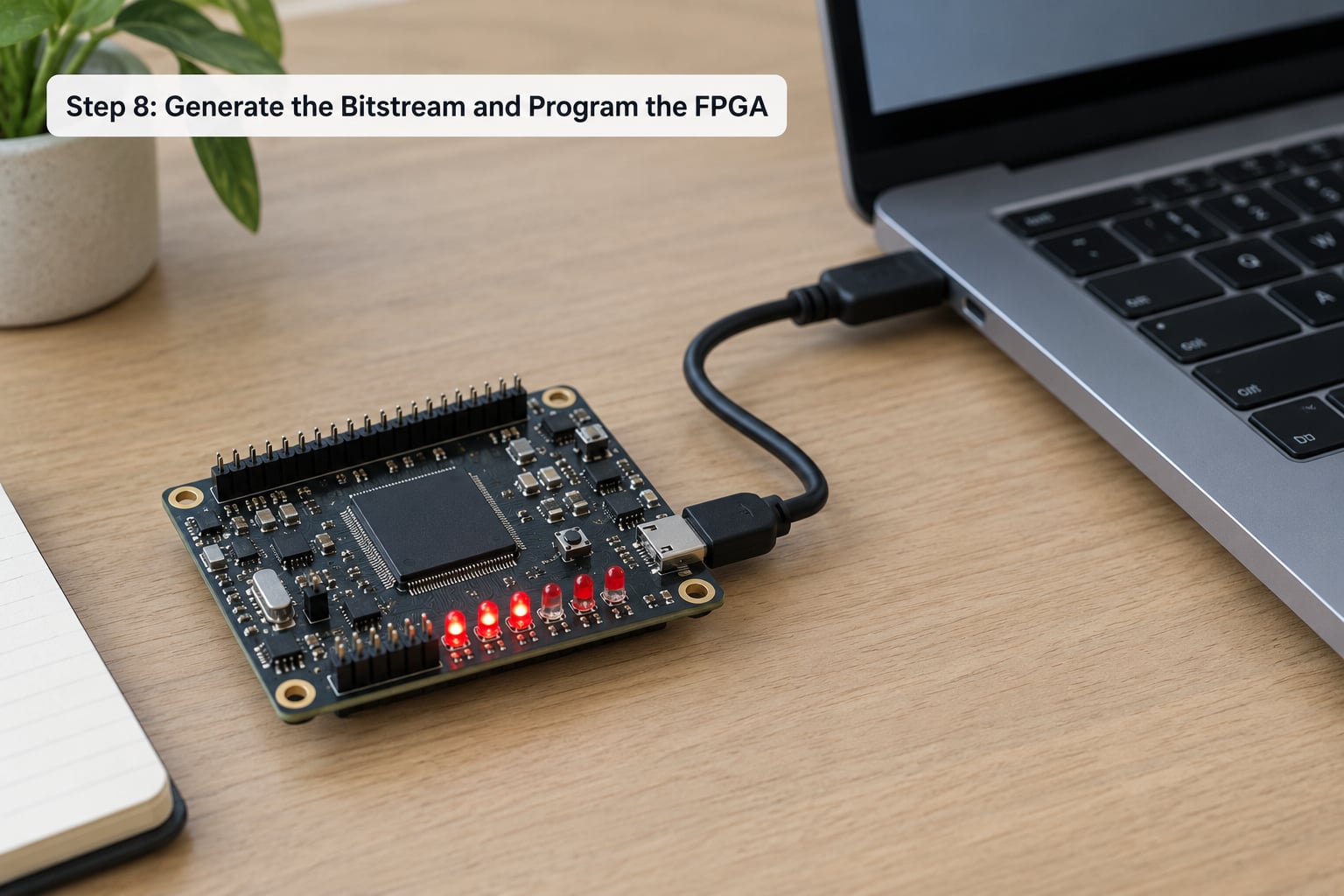
In Vivado, generating the bitstream is a click on Generate Bitstream in the same Flow Navigator where you ran synthesis. In Quartus the equivalent is Compile, and on Lattice boards it is Export. The output is a .bit file for Vivado, a .sof or .pof for Quartus, and a .bit or .hex for Lattice.
Programming goes through the board’s on-board JTAG interface, which is a serial link that the host uses to configure the device. In Vivado that is the Hardware Manager: open the target, auto-connect to the board, select the bitstream, and program the device. The manager also shows a DONE signal, which is how you know configuration actually completed rather than merely started.
Two different things get programmed, and beginners conflate them. The FPGA bitstream configures the logic fabric itself. The board’s configuration flash, if it has one, stores that bitstream so the board comes up programmed without a host attached. For a first project, always program the FPGA directly and skip the flash step.
Step 9: Validate on Hardware and Iterate
Bring-up is a sequence, not a leap of faith. Reset the board, apply power, check the 3.3 V rail, then program. After configuration, check the DONE light and then the four LEDs. If the count is wrong, do not start rewriting RTL, because the most common causes are physical.
Work down this list: the clock pin is wrong, the reset is active-low and you forgot to release it, the LED pins are mismatched or the board’s LEDs are active-low, or the I/O standard mismatches the bank voltage. Each takes a minute to check in the constraint file and each one produces a dead or nonsensical display.
When the simple design works, the way to debug anything harder is an on-chip debug probe. An integrated logic analyzer watches internal signals while the design runs and streams them to the host over JTAG, so you can see a live counter, a state machine’s transitions or an interface handshake without a scope or a redesign. It costs a few minutes to insert and it replaces most of the guesswork in bring-up.
Once validation passes, write down what you observed and what you would change next, then archive the project and its bitstream with the version control history attached. When something fails three weeks later, that archive answers the only question that matters: which source, constraints and tool version produced a bitstream that behaved a certain way.
A sensible project progression, so the next design is not a leap: blink one LED, then the 4-bit counter on four LEDs, then a switch-driven counter, then a PWM output, then a UART transmitter, then a UART receiver, then a small FIFO, then an I2C or SPI master, and only then anything resembling a processor. Each step adds one new concept and reuses everything before it.
Common Mistakes in the FPGA Design Flow
These are the failures that appear again and again, and the symptom usually shows up somewhere other than the cause.
| Mistake | Symptom you see | Fix |
|---|---|---|
| No clock constraint in the XDC, QSF or LPF file | Wildly negative slack, or an implementation that fails outright | Add create_clock with the real board clock period |
| Pin numbers copied from a different board or revision | Nothing happens, or LEDs light in the wrong order | Take every pin from your board’s user manual pin table |
| Wrong reset polarity | Design stays frozen at its reset value | Match the active level in the constraint file to the code |
| Blocking assignment inside a clocked always block | Simulation works, hardware gives wrong results | Use non-blocking assignment for all sequential logic |
| Combinational always block with no else branch | Latch inference warning after synthesis | Assign a default at the top of the block |
| Testbench code pasted into the synthesizable set | Synthesis errors about delays or $display | Keep the testbench in a separate file excluded from synthesis |
| Ignoring warnings in the report | Works at low speed, fails timing after you add features | Treat latch and unconnected-port warnings as errors |
| Crossing clock domains without synchronisation | Rare, random data corruption on hardware only | Use a two-flop synchroniser or a proper asynchronous FIFO |
| Jumping to hardware before simulating | Hours lost debugging logic that a testbench would have caught | Simulation is seconds. Always run it first |
| Copy-pasting IP without checking its licence | Blocked from commercial release later | Check the licence of every IP block before you depend on it |
The clock domain one deserves emphasis. If two parts of your design run on unrelated clocks and you sample a signal across between them without a two-flip-flop synchroniser, you will get a metastable value occasionally. It may happen once in a million cycles, which is exactly the kind of bug that never reproduces on the bench and always shows up in the field.
Frequently Asked Questions
What is the FPGA design flow?
It is the fixed sequence of stages used to turn a hardware idea into a working FPGA: requirements and architecture, RTL design entry, functional simulation, synthesis, constraint application, place and route, bitstream generation, and programming plus board validation. The stages are the same for every vendor and every device. Only the tool names and menu labels change between Vivado, Quartus and Lattice toolchains.
What is the first step in FPGA design?
The first step is requirements definition, and it is a document rather than a tool action. You write down the clock source and frequency, reset style, every external interface and its I/O voltage, the expected resource use, the timing target and the pass criteria. RTL written before that list exists tends to be rewritten, because the interface changes as soon as you meet the board.
What is the difference between synthesis and implementation in FPGA?
Synthesis converts your RTL description into a netlist mapped onto FPGA primitives such as lookup tables, flip-flops and block RAM, and it produces a utilization report. Implementation takes that netlist and physically places and routes it on the device, then produces a timing report. A design can synthesize cleanly and still fail implementation on timing, pin assignment or routing, so both stages have to pass.
What is a bitstream file in FPGA?
A bitstream is the configuration file that programs an FPGA’s fabric. It encodes which lookup tables hold which truth tables, where registers start, and how the routing resources are connected, turning blank configurable silicon into your circuit. On Vivado it is a .bit file, on Quartus a .sof or .pof, and on Lattice tools a .bit or .hex. Without a bitstream the device does nothing at all.
Which HDL should I learn first: Verilog or VHDL?
For most beginners, Verilog or SystemVerilog is the faster start because most free tutorials, example code and board documentation use them, and Vivado supports both with good testbench tooling. SystemVerilog adds assertions and stronger typing, which pays off once your first design works. Choose VHDL instead if your course, employer or industry standard already uses it, since the design flow is identical either way.
What is an FPGA constraint file (XDC, UCF, QSF)?
A constraint file tells the tool how your logical ports connect to the physical device. It holds pin assignments, I/O standards and voltage levels, and the clock period your design must meet, plus optional placement and timing exceptions. Vivado uses XDC, Quartus uses QSF and older Xilinx flows used UCF. The same roles, different file extensions, which is a common trip-up when you follow a dated tutorial.
Do I need a development board to learn FPGA?
You can learn most of the flow without hardware. Writing RTL, building a testbench, running simulation, and reading synthesis and timing reports all work in a free simulator and synthesis tool, and a decent number of the open-source tools run entirely on a laptop. A board does add something real though: it is the only way to learn about pin constraints, clocking, I/O standards and bring-up, which is where a surprising share of real bugs live.
Conclusion
Start with a 4-bit counter on four LEDs and take it all the way through: requirements, RTL, a testbench you watch pass, synthesis with the reports actually read, constraints from your board manual, implementation, a positive timing report, a bitstream, and LEDs that count. That single project touches every stage of the FPGA design flow and gives you a working baseline to build on.
Then go one concept at a time, in the order that reuses the most from what you already have. The tools will keep improving around you, but the flow will not change.