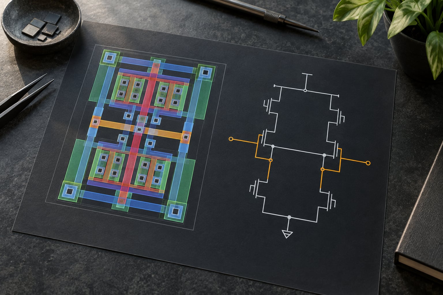
A layout versus schematic check, usually shortened to LVS, is the physical verification step that proves the netlist extracted from a chip layout is electrically the same circuit as the netlist generated from the schematic. The tool pulls devices and nets out of the layout geometry using the foundry’s device recognition rules, matches them against the source design, and returns a MATCH or MISMATCH verdict before anyone spends money on a wafer.
One note before we go further, because it trips up a lot of readers. This is about integrated circuit layout. Several pages ranking for “schematic vs layout” are really about printed circuit boards, where a Gerber file is compared against a netlist by a different class of tool. The ideas overlap, but the geometry, the rules decks and the failure modes are not the same. What follows is the IC version.
Table of Contents
- Layout Versus Schematic Check Explained at a Glance
- What Is a Schematic Check?
- What Is a Layout Check?
- What Does Layout Versus Schematic Verification Compare?
- Step 1: Prepare the layout database
- Step 2: Extract the layout netlist
- Step 3: Generate the schematic netlist
- Step 4: Recognise and parameterise devices
- Step 5: Flatten and normalise
- Step 6: Compare and return a verdict
- How Device and Net Matching Works
- Source and drain symmetry
- Series and parallel folding
- Device size tolerance
- Dummy and filler devices
- Black boxes and abstract devices
- Hierarchy
- What Is the Difference Between LVS and DRC?
- Which Check Should You Run First?
- How to Read Common LVS and Layout Errors
- Which Should You Choose?
- Frequently Asked Questions
- Is LVS the same as a schematic check?
- What does LVS compare in an IC layout?
- Should DRC or LVS run first?
- Why does LVS report a mismatch when the schematic looks correct?
- Does LVS check transistor dimensions?
- What files and PDK data are needed for layout verification?
- Conclusion
Layout Versus Schematic Check Explained at a Glance
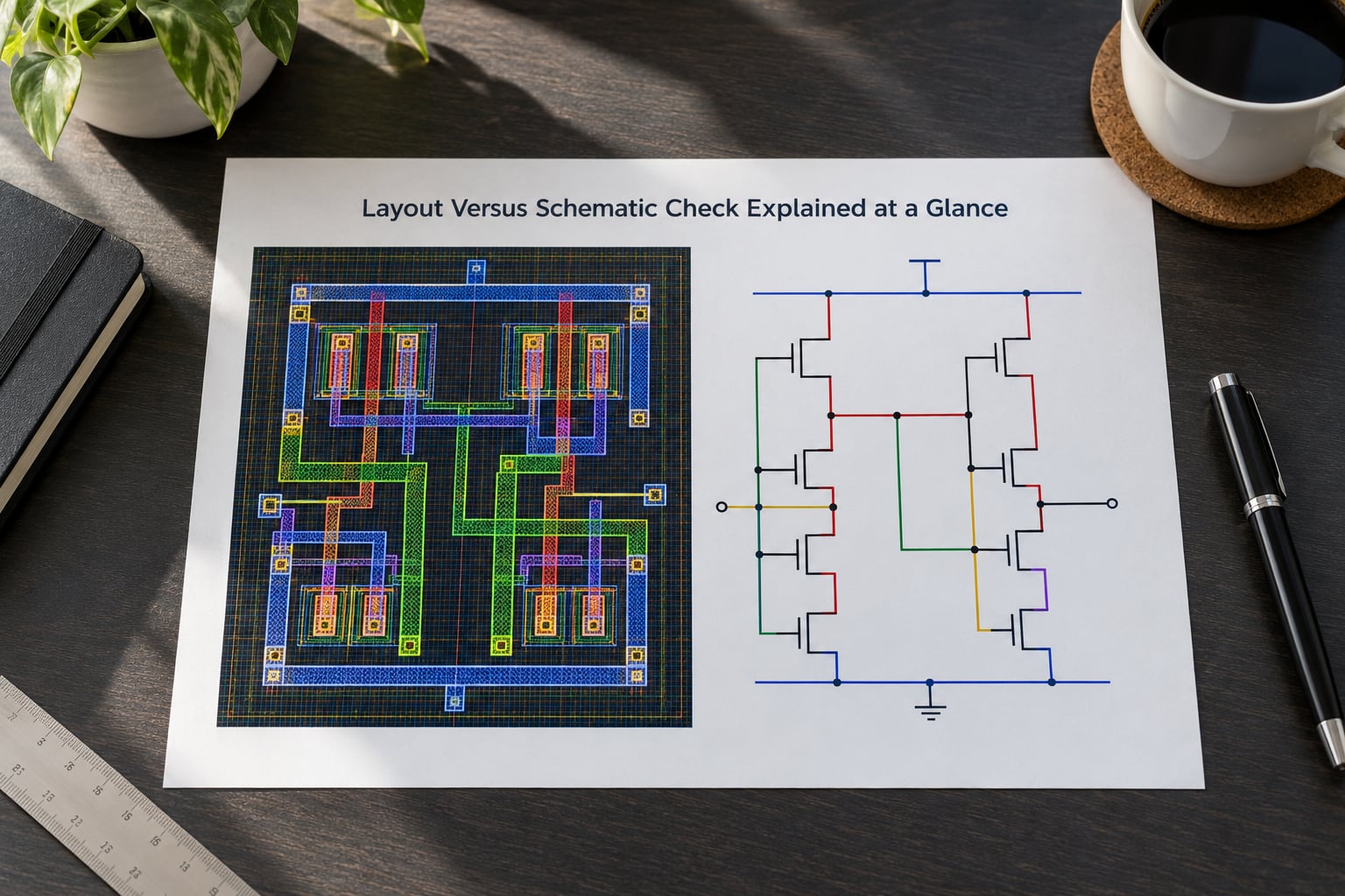
Three checks get confused constantly, so here they are side by side. The schematic check asks whether the design intent is sane. The layout check asks whether the geometry can be manufactured. LVS asks whether the geometry implements the design intent.
| Aspect | Schematic check | Layout check (DRC) | LVS |
|---|---|---|---|
| Purpose | Confirm the design intent is electrically valid | Confirm the geometry obeys fabrication rules | Confirm the layout implements the intended circuit |
| Design inputs | Schematic source, cell libraries, constraints | Layout database plus a foundry rule deck | Layout database plus a device recognition deck and the source netlist |
| Connectivity analysis | Optional ERC pass on named nets and power domains | None, beyond a few antenna and density checks | The core operation, done as graph matching |
| Device recognition | Devices come from symbols in the source | None, devices are not a DRC concern | Devices are recognised from geometry, then parameterised |
| Physical rule checks | Not applicable | Spacing, width, enclosure, density, antenna | Only the subset of geometry rules the device deck needs |
| Extracted parameters | Nominal values from the source | None | Width, length, multiplicity, capacitance and resistance where the deck extracts them |
| Typical tools | ERC in the schematic editor, SPICE simulators | Calibre, Cadence Assura, Synopsys IC Validator, Magic | Calibre nmLVS, Cadence Assura LVS, Synopsys, Magic with Netgen |
| Signoff role | Gate before layout starts | Manufacturing gate at every iteration | Electrical equivalence gate before tapeout |
Read the last two rows together. DRC and LVS both run against the same layout database and both need a foundry deck, which is exactly why teams assume one is part of the other. They are separate engines with separate decks and separate verdicts.
What Is a Schematic Check?
A schematic check starts from the schematic, the symbolic view of the circuit. Every device, wire, port and parameter in that drawing is an intentional statement about what the silicon is supposed to do.
What a schematic check actually verifies depends on the shop. At minimum it is a review of electrical rules: are the supply domains consistent, is every input driven, are the MOS bulk terminals tied correctly, are there any floating nodes. A formal electrical rule check, usually shortened to ERC, automates part of that.
Beyond rules, the schematic side is where you simulate. A SPICE simulation of the schematic tells you the gain, the bias point, the settling behaviour. That is a functional statement, and no geometry check anywhere in the flow can make it for you.
The key limitation to hold onto: a clean schematic says nothing about whether the person who drew the layout built that same circuit. Wires cross on a schematic without consequence. In metal they short.
What Is a Layout Check?
A layout check works on geometry. The layout is polygons on named layers, cut by vias, bounded by design rules that come from the process. A layout check reads those polygons and measures the distances between them.
Typical rules include minimum spacing between different nets, minimum wire width for the layer, enclosure of a via by the metal above and below it, density windows so that a region is not too sparse or too crowded, and antenna ratios that limit how much gate area a single metal wire can charge.
DRC, design rule checking, is the tool that enforces those rules. It reports coordinates and rule names, and it is fast, which is why it runs continuously through the whole layout phase.
Here is the problem with geometry-only inspection. A layout can be perfectly clean and still be the wrong circuit. Two nets can be spaced a micron apart, no rule broken, and if one of those spaces closes during a later fill operation you have a short that no DRC run will ever report. DRC asks whether the geometry is legal. It cannot ask whether the geometry is correct.
What Does Layout Versus Schematic Verification Compare?
Now the actual answer to how LVS works. The comparison is done in six stages, and the order matters because each stage consumes the output of the last one.
Step 1: Prepare the layout database
The layout is streamed to the LVS tool, usually a GDSII or OASIS database. If you have an internal database it gets converted first. This step also handles cell hierarchy, since the tool needs to know which repeated cells can be compared as a unit rather than flattened into millions of polygons.
Step 2: Extract the layout netlist
Using the foundry’s device recognition deck, the tool scans for the geometry patterns that mean “this is a transistor” or “this is a metal-over-metal capacitor”. For each pattern it records the connecting terminals, the net names it inferred, and the parameters it can measure such as width and length.
Everything the tool could not recognise is simply absent from the output. That is the single most common reason a beginner sees an empty layout netlist on a design that is otherwise fine.
Step 3: Generate the schematic netlist
The source design is simulated out to a flat or hierarchical SPICE netlist. This is the reference side. Its device names come from the schematic, its parameters come from the symbols and their properties.
Step 4: Recognise and parameterise devices
Both sides go through normalisation. The layout device becomes a primitive with terminals in a known order. Bipartite matching is applied where a device may legitimately match in more than one way, such as a symmetric MOS transistor whose source and drain can swap. Devices that are functionally equivalent but built differently, a series stack implemented as one device, or two devices merged, get folded under the deck’s rules.
Step 5: Flatten and normalise
Hierarchy is collapsed for comparison, names are discarded, and both netlists are reduced to a canonical form. From this point on, identity comes from structure alone. A net in the layout called net_4173 has no more claim to a name than one called VDDA.
Step 6: Compare and return a verdict
The two normalised netlists are matched as connectivity graphs. Devices are paired by type, parameters and terminal connections; nets are paired by which device terminals they touch. The result is MATCH, or MISMATCH with the unmatched devices and nets named and usually cross-referenced back to layout coordinates.
It is worth being explicit about what that verdict does not mean. LVS does not check that the circuit functions. It does not check timing, it does not check signal integrity, it does not check power integrity, and it does not check that the extracted resistance and capacitance values are small enough. A chip that passes LVS with a match can still be far too slow, because the netlist it matched was the correct circuit built out of far too much wire.
Engineers on r/chipdesign describe LVS as the first real gate between “the layout looks right” and “the chip will be the circuit you drew”. That framing is accurate, and it is also the reason people expect more from it than it delivers.
How Device and Net Matching Works
Because matching is structural, a handful of rules explain almost every surprise in a report.
Source and drain symmetry
A MOS transistor is symmetric as far as LVS is concerned, unless the deck says otherwise. A layout where the source is where the schematic drew the drain will still match, and that is correct behaviour, not a missed error. Moment and other orientation-dependent effects are a simulation question, not an LVS question.
Series and parallel folding
Two transistors in series on the schematic can appear in the layout as a single device with a different geometry, or as two devices with a shared node. Whether that matches depends on the folding rules in the device recognition deck. When a report shows a parameter mismatch on a stack, this folding rule is usually the reason.
Device size tolerance
Some decks allow a relative tolerance on width and length, some allow none. A device drawn 2% larger than the schematic will match on a tolerant deck and fail on a strict one. This is the difference between a parameter-level mismatch and a connection-level mismatch, and the report tells you which one you have: parameters listed with a size delta is the first, a missing or extra terminal is the second.
Dummy and filler devices
Analog and mixed-signal blocks are full of devices that are drawn in the layout for manufacturing reasons and exist in the schematic as nothing, or as a named dummy. If the deck does not have an ignore rule for them, every one shows up as an unmatched layout device. The same applies to filler cells added for density.
Black boxes and abstract devices
When a block is not available at the current level of hierarchy, the netlist uses a subcircuit call or a black box. LVS compares the interface, meaning the pin set and the connectivity around it. It does not look inside. The flip side is that a black box can hide an entire wrong circuit, which is one reason the flow discourages using them more than necessary.
Hierarchy
A hierarchical comparison matches a cell once and reuses the result, which is why a full-chip run is often minutes rather than hours. A cell that matches at the top level is assumed to match everywhere it is instantiated. If a block matches only sometimes, the report will say the cell matched in one context and not another, and the differing net is the place to start.
What Is the Difference Between LVS and DRC?
DRC is design rule checking, which asks whether the geometry can be fabricated without breaking the process. LVS is layout versus schematic checking, which asks whether the geometry implements the intended circuit. Different question, different input deck, different verdict.
| Dimension | DRC | LVS |
|---|---|---|
| Question answered | Is the geometry legal? | Is the geometry the right circuit? |
| Primary input | Layout database plus rule deck | Layout database, device deck and source netlist |
| Deck type | Layer rules, spacing and width constraints | Device recognition and parameter extraction rules |
| Typical findings | Spacing violations, width violations, via enclosures, density, antenna | Shorted nets, open nets, missing devices, size mismatches, swapped pins |
| Does it look at connectivity | Not as a goal | Yes, that is the whole job |
| Typical cadence | Every iteration, in the background | Milestones and signoff, plus early dirty-design runs |
| Result if it fails | Manufacturing will produce defects or the fab will reject the database | The fabricated chip will not be the circuit that was designed |
The practical consequence is that a clean DRC run tells you nothing reassuring about LVS, and a clean LVS run tells you nothing reassuring about DRC. They are independent gates and both have to pass.
There is a third check that gets lumped in here. Electrical rule check, or ERC, runs on the schematic before layout exists, and it is the source-side counterpart to LVS. Some flows also run an antenna check and a layout-versus-extracted check, where the extracted netlist including resistance and capacitance is compared against the layout netlist. Same family of idea, wider scope.
Which Check Should You Run First?
Both, early and often. The ordering people usually get wrong is assuming LVS only makes sense once the layout is nearly finished, which is how teams end up facing tens of thousands of errors at once.
At early implementation, when a block is partially routed, run both. DRC on the routed region and LVS on a small test structure or a single leaf cell. The point at this stage is not the verdict, it is proving that the device recognition deck recognises your devices at all. An early check that comes back with an empty layout netlist is a deck problem you can fix in a day, and finding that out three weeks later is a schedule problem.
At midstream integration, when full blocks are laid out, run LVS per block rather than at the top level. Block-level comparison is where the report is still readable, and a block that matches on its own usually matches in context. If a top-level run does fail, the tool points back to the cell, and you debug once instead of chasing a single symptom through a million-gate hierarchy.
At signoff, run the full foundry signoff decks. This is the run that goes to the foundry, and it uses the foundry’s own rule and device decks rather than the in-house versions you used during development. Differences between an internal deck and the foundry deck are a real and recurring source of late surprises.
Between milestones, when a design is dirty and connectivity is still moving, the useful technique is short isolation. Instead of a full comparison, the tool groups the shorted paths so you can see which single short is causing a cascade. Siemens reported working with a 5nm design containing over 15,000 shorts, and their tooling claims a six to ten times faster turnaround on that kind of case than repeated full LVS runs. The number is vendor data, but the direction is right: on a dirty design, isolate the shorts instead of rerunning everything.
How to Read Common LVS and Layout Errors
Most reports are short once you know the shape of them. The table below maps the message to what it usually means and what to do about it.
| Error | Usual cause | What to check |
|---|---|---|
| Shorted net, two layout nets merged | A spacing violation that DRC did not cover, often from fill, a via array or an illegal merge | The highlighted layout coordinates; check whether the region is inside a fill or density block |
| Open net, device terminal unconnected | A missing via, a via on the wrong layer, or a connection made on a layer the deck does not extract | Whether the via stack actually touches both nets at each layer |
| Device not recognised, appears only in the schematic | The geometry pattern does not match any entry in the device recognition deck | The device geometry against the deck, including required enclosure and implant layers |
| Layout netlist is empty or nearly empty | A wrong or missing deck, wrong layer numbers, or a units and database conversion problem | Layer mapping and database units first, before suspecting the layout |
| Size mismatch, width or length off by a factor | A device drawn with a different multiplier, or series and parallel folding applied differently on the two sides | The multiplier in the symbol against the drawn geometry, then the deck’s folding rules |
| Swapped or reordered pins | A subcircuit or black box interface defined in a different order, or a symmetric device matched the other way round | Whether the device is genuinely symmetric before treating it as an error |
| Unmatched dummy or filler device | Filler added for density, or an analog dummy drawn in layout but absent from the schematic | Whether the deck has an ignore rule for that class of device |
| Power domain mismatch | Two supply labels that are not joined in the schematic but are physically the same metal in the layout, or vice versa | Global connection declarations, not the metal |
The passive device row is the one that costs beginners the most time. A metal-over-metal capacitor, a MOS capacitor built from a gate, a poly contact resistor, a via stack used as an inductor, each needs a correct entry in the device recognition deck before it can ever appear in the layout netlist. A designer on r/chipdesign laid out a 5 by 5 micron interdigitated MOM capacitor, got a clean DRC, and could not pass Calibre nmLVS because the extracted netlist contained nothing. The layout was fine. The deck had no recognition rule for that device.
Two habits make these reports much faster to work through. Read the first mismatch rather than the last, because the first one usually causes several of the rest. And keep the GUI results viewer and the command line in the same workflow, since most of the actual fixing happens in the layout editor, not in the report.
Which Should You Choose?

You are not choosing one. The checks answer different questions and the question you are actually asking decides which one you are looking at.
If you are asking whether the design itself makes sense, that is a schematic check. Simulation and ERC answer whether the circuit functions as intended, before a single polygon exists.
If you are asking whether the foundry can build it, that is DRC. Spacing, density and antenna rules decide whether the wafer comes back working.
If you are asking whether you built the circuit you designed, that is LVS, and it is the only one of the three that compares against the intent.
If you are asking whether you are ready to tape out, you need all of them plus the foundry signoff decks, the antenna check, extracted simulation and static timing analysis on the extracted netlist. LVS is one gate in that set.
For students and small teams without foundry licences, the open-source path is real rather than a consolation prize. The sky130 PDK with the OpenLane flow, Magic for layout and extraction and Netgen for comparison gives a complete LVS loop you can actually iterate on. Magic and Netgen are not equivalent to the foundry signoff decks in tolerance handling or in device coverage, and no commercial flow can be replaced by them for a tapeout, but they teach the loop properly. Several of the questions that come up most often on chip design forums come from people learning on exactly that stack.
One last practical note. If your flow is automated, wire LVS into CI with a non-zero exit code on mismatch. A run that reports errors and returns success is worse than no run at all, because it teaches the team to ignore it.
Frequently Asked Questions
Is LVS the same as a schematic check?
No. A schematic check works on the source design, checking electrical rules, connectivity intent and simulation results before layout exists. LVS works on the physical layout, extracting devices and nets from geometry and comparing them with the netlist generated from the schematic. One proves the design intent is valid, the other proves the layout implements it.
What does LVS compare in an IC layout?
It compares devices and nets. On the layout side it extracts recognised devices with their terminals and parameters, then infers connectivity. On the schematic side it takes the SPICE netlist. Both are flattened and matched as connectivity graphs, and the result is a MATCH or MISMATCH naming the unmatched devices and nets.
Should DRC or LVS run first?
Run both, and neither gates the other. DRC runs continuously through layout because it is fast and cheap. LVS is most useful at milestones: a small early run to confirm the device deck recognises your devices, a per-block run during integration, and a full signoff run with foundry decks before tapeout. A block that is not DRC clean can still be usefully LVS checked.
Why does LVS report a mismatch when the schematic looks correct?
Usually the layout, not the schematic. The most common causes are a shorted or open net, a device whose geometry does not match any entry in the device recognition deck, a passive such as a MOM capacitor that the deck does not recognise, or a wrong layer mapping producing a nearly empty layout netlist. A mismatch message naming only layout-side devices usually means deck or mapping, not circuit intent.
Does LVS check transistor dimensions?
It checks them, with tolerance that depends on the deck. A device drawn slightly larger than the schematic may pass on a tolerant deck and fail on a strict one. LVS compares width, length, multiplicity and extracted values, and reports a parameter mismatch separately from a connection mismatch. It does not care about effects that depend on orientation, such as source and drain asymmetry in a MOS device, because those are treated as symmetric.
What files and PDK data are needed for layout verification?
You need the layout database, usually GDSII or OASIS, a foundry or PDK rule deck for DRC, a device recognition deck for LVS that covers every device type you used, and the schematic or SPICE netlist. For signoff you need the foundry decks, which are usually under NDA. Open PDKs such as sky130 ship with both rule and device decks, which is why they work for learning and for hobby silicon.
Conclusion
Layout versus schematic check explained in one line: LVS extracts the netlist from your layout geometry and compares it against the schematic netlist to prove the chip you are about to fabricate is the circuit you designed. DRC checks that the geometry is manufacturable, and a schematic check checks that the design intent is valid, so all three run together rather than one replacing the others.
The first thing to do, whether you are starting a block or debugging a report, is run LVS on one small leaf cell with the device recognition deck you intend to use. If the layout netlist comes back empty, you have a deck or layer mapping problem, and you can find it in an afternoon rather than a week. Everything after that, the 2026 signoff flow included, is an extension of the same comparison.