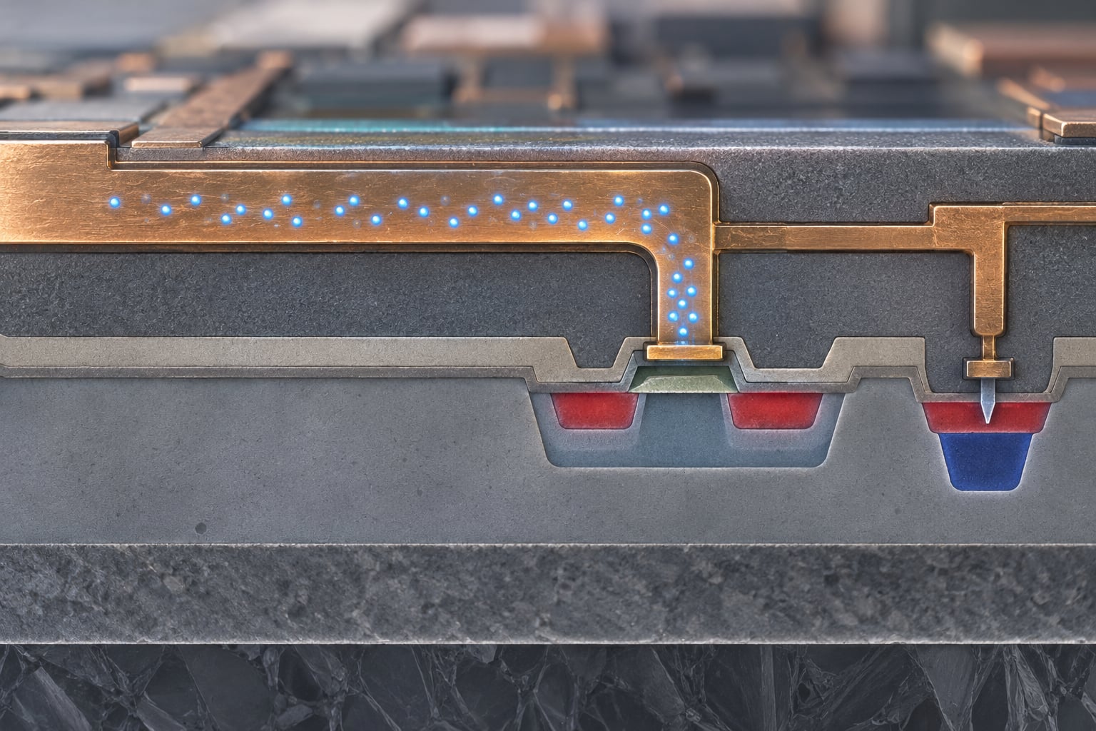
The antenna effect in chip layout is plasma-induced gate oxide damage. Charge builds up on a wide metal wire during plasma etching, and when that wire is hooked to a MOS gate with no grounded path yet, the charge forces its way through the thin gate oxide and damages the transistor. Fabs limit it with metal-to-gate area ratio rules, and engineers clear violations with antenna diodes, metal jumpers or dummy transistors.
The name is misleading, and it sends people down the wrong path. There is no radio antenna anywhere near your layout. The “antenna” is simply the piece of metal whose large surface area collects charge from the etch plasma, and the antenna effect is what happens when that collected charge discharges somewhere it should not.
Below is the mechanism, the structures that trigger it, the arithmetic behind the rules, and the fix techniques, in the order a physical design engineer meets them.
Table of Contents
- What Is the Antenna Effect in Chip Layout?
- The Antenna Effect in Chip Layout: The Core Mechanism
- Why Does the Antenna Effect Cause Transistor Failures?
- Which Layout Structures Create the Problem?
- How Do Engineers Calculate the Antenna Ratio?
- How Do You Fix the Antenna Effect in Chip Layout?
- How Can You Prevent Antenna Problems During Design?
- Frequently Asked Questions
- What is the antenna ratio in VLSI?
- Which layers are covered by antenna rules?
- Why does an antenna diode have to be close to the gate?
- Does the antenna effect still matter at 7nm and 5nm?
- Does DRC catch antenna violations automatically?
- What to Do First
What Is the Antenna Effect in Chip Layout?
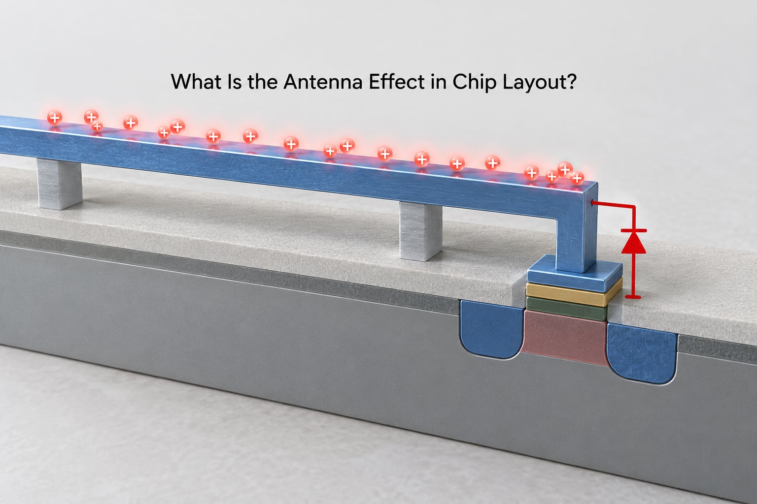
In one sentence: the antenna effect is damage to a MOS gate oxide caused by charge that accumulates on a large connected metal area during plasma etching and then discharges through that gate.
Every chip goes through a long sequence of front-end and back-end steps. During the front-end of line (FEOL) the transistors, gate oxide and source/drain diffusions are built. During the back-end of line (BEOL) the metal stack is deposited, patterned and polished. Patterning metal means removing it with plasma etching, and plasma etching is the source of the trouble.
The affected device is the transistor whose gate is electrically connected to the charged metal. Not the transistor sitting under the biggest wire, not the ones nearby, the specific one whose gate terminal shares the connection. Damage shows up as a shifted threshold voltage, extra leakage, or a permanently broken dielectric.
The Antenna Effect in Chip Layout: The Core Mechanism
Here is the sequence, step by step, and it is worth following slowly because each step explains the next.
- Deposition. A metal layer is laid down over the wafer. If it covers a MOS gate, that gate now shares the metal’s electrical node.
- Plasma etching. Reactive ion etch uses an ionised gas between two electrodes. Ions and radicals hit the wafer at hundreds of electron-volts. Metal shapes that survive the etch stay exposed to this bombardment, and photoelectrons and ions land on them.
- Charge collection. A conducting surface floating in that plasma charges up until the sheath around it pushes back. A wide, thick wire presents a large collecting area, so it gathers far more charge than a narrow one.
- No escape route. If the gate is not yet connected to a source/drain diffusion, there is no junction to bleed the charge off. The node floats and its potential climbs.
- Oxide stress. Charge on the gate terminal means charge across the gate dielectric. Once the field exceeds what the oxide can take, electrons tunnel through, trap in the oxide, or punch a permanent hole.
- Dielectric charging, not always breakdown. Most gates survive the excursion with trapped charge and no hole at all. That gate still fails the design, because a shifted threshold is a shifted threshold.
The useful mental model: the charged metal behaves like a distributed voltage source feeding the gate, not a lumped capacitor sitting on top of it.
Why Does the Antenna Effect Cause Transistor Failures?
Because the gate oxide is one of the thinnest, most perfect insulators in the whole fab, and it is asked to hold a voltage it was never designed to hold.
Every chip passes through dozens of plasma steps. A small amount of charging is normal and harmless. The distinction that matters is between ordinary transient charging, which every device experiences, and accumulated charge large enough to push the oxide past its limits. The antenna ratio exists to keep the second case out of the process.
The consequences, in rough order of how quickly they show up:
- Gate oxide breakdown. A conductive filament forms through the dielectric and the gate leaks hard. The transistor is dead and usually the whole node is dead with it.
- Charge trapping and threshold voltage shift. Electrons stuck in the oxide push the effective threshold around. It may be low enough to pass the functional test and drift out of spec a year later.
- Mobility degradation. Trapped charge scatters carriers, so transconductance drops. Timing and drive current suffer even where the logic still passes at room temperature.
- Increased gate leakage. A thinned or damaged oxide tunnels badly. On a low-leakage design this quietly destroys the power budget.
- Shortened device lifetime. Repetitive oxide stress wears the dielectric out. Field failures arrive at the customer instead of at the test house.
That last one is why antenna DRC blocks tapeout rather than sitting in a warning bucket. An antenna violation is not a marginal timing problem you can close at the last minute; it is a latent manufacturing defect the foundry has decided not to absorb.
One counterintuitive footnote from the literature: thin oxides were once considered more vulnerable here, since the same voltage across a thinner film gives a stronger field. Modern high-k gate dielectrics with metal gates changed that trade-off, and thin-oxide damage behaviour is now routinely characterised in qualification rather than assumed.
Which Layout Structures Create the Problem?

High antenna risk comes from two things multiplied together: a big collecting area and a small connected gate. Structures that produce one or the other are where violations cluster.
- Large MOS gates. Input/output pads, ESD clamps and level shifters use fat transistors for current handling. Those gates are large, but they usually have short, thick connections, so the ratio stays manageable.
- Long and wide metal wires. A long route on M1 feeding a minimum-size gate in a standard cell is the classic violation. This is the case almost every foundry flags.
- Polysilicon connections. Where polysilicon crosses a thin-oxide area, the polysilicon itself acts as an antenna before any metal is involved. Poly rules are checked separately from metal rules for exactly this reason.
- Vias and stacked connections. Each via stack adds collecting area to the same node. A single gate connected up through four metal levels carries the accumulated ratio of all four.
- Analog and custom blocks. Analog routing is wide, manual and often uses unusual layer combinations. Bias lines and current mirrors that must match exactly are exactly the kind of geometry that gets flagged.
- Memory periphery. Word and bit lines are long, and the sense amplifiers they drive have small gates. Flash-style charge pump arrays are the classic stress case.
- NWELL antenna effect. Practitioners on semiconductor forums report this variant is more dominant than its metal counterpart. Because an NWELL is tied through well contacts rather than a small diffusion, a large well area tied to a gate can carry higher potential and more charge into the same gate terminal, and fewer of the usual fixes apply cleanly.
The pattern to notice: everything above is a connectivity question, not a device question. The DRC error reports a net, and the fix always changes what that net touches.
How Do Engineers Calculate the Antenna Ratio?
The antenna ratio is the total area of wire connected to a gate, divided by the area of the gate itself. If the connected metal is 300 square micrometres and the gate is 1 square micrometre, the ratio is 300 to 1.
The formula is simple. What makes it fiddly in practice is which areas get counted.
Per-layer ratio. Connected wire area on one layer divided by gate area on that layer. This catches the obvious “long M1 into a small gate” case.
Cumulative ratio. All connected wire areas across every layer, summed, divided by total connected gate area. This is the rule that catches deep via stacks and the one most often missed.
Periphery or diffusion-connected rules. Some rules measure the gate area against the connected wire area with a relaxed threshold, on the grounds that once the gate is tied to a source/drain diffusion there is a junction to absorb the charge. The tool has to know whether the diffusion is there at the layer being checked.
| Rule type | What it compares | Catches |
|---|---|---|
| Per-layer | Connected wire area on one layer vs gate area on that layer | The obvious long-wire violation |
| Cumulative | All connected wire areas vs total connected gate area | Deep via stacks and multi-level routing |
| Periphery / diffusion-connected | Wire area vs gate periphery, accounting for diffusion connection | Cases where a junction already bleeds charge |
A worked example, with illustrative numbers since rule values vary by node and foundry. Take a standard cell input gate of 1 square micrometre connected to 250 square micrometres of M1 and 60 square micrometres of M2. The cumulative ratio is 310 to 1, against a typical cumulative limit in the low hundreds for a mature node. That is a violation.
Now take the same cell and jump a piece of M2 down to M1 about two microns from the gate, then drop a diffusion diode at the gate. The diode is forward biased by the charging plasma and diverts charge; the hop breaks the M2 into a separate, smaller connected area. Re-extract and the ratio drops below the limit.
The lesson is that you can compute the fix before you draw it. Calculate the projected ratio, subtract the diode’s collection and the split metal area, and check you are still clear before you spend time in the router.
How Do You Fix the Antenna Effect in Chip Layout?
There are three standard techniques. Which one you pick depends on how much margin you need, how much area you can afford and how much of the net you can restructure.
1. Metal hopping, also called jumper insertion. Drop the offending net to a lower metal layer for a short segment, then bring it back up. The single net is now two smaller antennae instead of one large one, and the cumulative ratio falls. It costs routing flexibility and a little capacitance, and in congested advanced nodes there may be nowhere to put the hop.
2. Antenna diode insertion. Add a diode-connected diffusion tied to the net. During plasma etch the diode conducts and drains charge away from the gate; during normal chip operation it is reverse biased and stays idle, costing almost nothing. This is the general-purpose fix and the one most commonly inserted.
3. Dummy transistor or floating gate attachment. Attach a deliberately floating gate to the net, or add a small transistor that adds gate area without adding a signal. Because the ratio is wire area over gate area, adding connected gate area is a direct way to bring the number down. It costs real area and can create an unwanted capacitive load.
| Technique | Extra area | Added capacitance | Best used when |
|---|---|---|---|
| Metal hopping | Low | Small to moderate | Routing has room and the violation is moderate |
| Antenna diode | Low | Minimal in normal operation | Default choice, especially at advanced nodes |
| Dummy or floating gate | Moderate | Noticeable | No routing room, or the gate area needs inflating anyway |
Two placement questions come up constantly, and the answers follow from the mechanism rather than from convention.
Why the diode must be close to the gate. Charge collecting on the metal between the gate and a distant diode has nowhere to go, because the wire is resistive. Practitioners describe that metal as a distributed voltage source, and the gate at the far end still sees the field. A diode ten microns away is barely better than no diode.
Input side or output side. Either works electrically as long as the diode sits on the same continuous metal as the gate with no intervening hop that would break the connection. The real constraint is physical: the diode must survive on the same metal the plasma reaches, and it needs a diffusion underneath it, which constrains where in the cell you can put it.
How Can You Prevent Antenna Problems During Design?
Antenna violations are cheap to avoid early and expensive to unwind at signoff. A workable order of operations looks like this.
Read the rule deck before you draw. Every process design kit ships its antenna rules with the layer definitions and the cumulative accounting. Know the limits for poly, M1, M2 and the top layer in your node before routing starts. Rules differ between foundries and between nodes, so the numbers in a tutorial are not the numbers in your PDK.
Run the antenna check early and often. Block-level antenna DRC after floorplanning catches the structural mistakes while they are still a drawing choice. Calibre, Assura and IC Validator all implement antenna rules from the foundry deck, and running them at block level rather than only at chip level is the single biggest time saver.
Keep routing discipline. Long thin routes into small gates are the whole problem. Prefer shorter connections to high-impedance or narrow-gate nodes, keep M1 usage modest on gate nets, and avoid unnecessary via stacks where a wider single layer will do the same job.
Review the ratio, not just the error count. Signoff teams often triage antenna errors by margin. A net at 90 percent of the limit is fine today and a problem the moment someone inserts an ECO route. Track your worst-case ratios as a metric during the block, because that is the number that tells you whether the block is genuinely clean.
Watch the analog and custom blocks. Standard cell libraries ship with antenna diodes already placed, because the library was characterised through the same rule deck. Bespoke analog routing does not. Those blocks need the most manual attention and the most signoff review.
Expect the rules to change at advanced nodes. Below roughly the 16nm generation the available metal area per gate rises as cells get denser and routing gets more vertical, and FinFET structures replace planar gates. Foundries respond with tighter cumulative rules and more stack-aware checks, so antenna discipline has to get more precise, not less, as geometry shrinks.
Where stacking and 3D integration add vertical connections to the same net, the cumulative accounting matters even more, because the antenna area can come from a layer the designer never drew on that die.
Frequently Asked Questions
What is the antenna ratio in VLSI?
The antenna ratio is the total area of metal or polysilicon wire electrically connected to a MOS gate, divided by the area of the gate itself. A ratio of 300 means 300 square micrometres of wire sit on a 1 square micrometre gate. Fabs publish maximum permitted ratios, usually both per layer and cumulatively across the stack, and antenna DRC fails the design when either limit is exceeded.
Which layers are covered by antenna rules?
Antenna rules normally cover polysilicon and every metal layer from M1 up through the top interconnect, checked both individually and cumulatively. Poly is checked on its own because polysilicon crossing a thin-oxide area collects charge before any metal is patterned. The cumulative rule matters most in practice, since a via stack quietly stacks the ratio of four layers onto one small gate.
Why does an antenna diode have to be close to the gate?
Because the metal itself is resistive, so charge collected between the gate and a distant diode has nowhere to discharge. Practitioners model that metal as a distributed voltage source feeding the gate, and the field at the gate end survives whatever the diode is doing at the other end. A diode a few microns from the gate clears the charge locally, which is why placement matters more than diode size.
Does the antenna effect still matter at 7nm and 5nm?
Yes, and the rules tighten rather than relax. Dense nodes offer more metal area per gate and more vertical routing, which raises the antenna area attached to any given gate. Foundries compensate with stricter cumulative ratios and stack-aware checking, and FinFET gate geometry changes the accounting again. Modern processes add antenna diodes into standard cell libraries for that reason.
Does DRC catch antenna violations automatically?
Yes, if your deck includes the rules. Calibre, Assura and IC Validator all read antenna rules from the foundry PDK and report the offending net with its ratio. What DRC does not do is judge whether your fix is sensible, so check that inserted diodes actually sit on the same continuous metal as the gate and are not separated from it by a hop.
What to Do First
Open your PDK rule deck and find the antenna section. Write the per-layer and cumulative limits for your node on the first page of your layout notes, then run antenna DRC at block level instead of waiting for signoff. Most antenna violations come from one long wire into one small gate, and most of those come from a routing decision made before anyone checked the ratio.