Non-recurring engineering, or NRE, is the one-time cost of getting a semiconductor product from a blank specification to production silicon: architecture and RTL design, verification, EDA and IP licensing, tape-out and mask sets, silicon bring-up, test, and packaging qualification. It is a fixed cost, paid once, that then gets spread across every part you build. For custom silicon at low or moderate volume, that per-part burden decides whether the project makes sense at all. This guide covers how vendors and industry analysts break down NRE costs in semiconductor projects, what actually drives them, and how to build a budget you can defend.
The numbers below are order-of-magnitude planning bands for US projects, not a national average and not a quote from any foundry or design house. Real pricing sits behind NDAs, so treat them as starting points for conversation. Wafer, packaging, and test costs are recurring and are not part of NRE, which is exactly where most budget confusion starts.
Table of Contents
- NRE Costs in Semiconductor Projects at a Glance
- How NRE Costs in Semiconductor Projects Are Estimated
- What Is Included in Semiconductor NRE?
- What Affects Semiconductor Project NRE?
- Cost Differences by Process Node
- How to Build a Project-Level NRE Budget
- Ways to Save Without Creating Production Risk
- Frequently Asked Questions
- Is there a standard national average for semiconductor NRE?
- Does semiconductor NRE include masks, IP, EDA tools, and packaging?
- Why does a leading-edge chip cost more to design than a mature-node chip?
- Can an FPGA prototype reduce the NRE budget for an ASIC project?
- Which semiconductor expenses are one-time rather than recurring?
- How much contingency should a first-time chip project budget for NRE risk?
- What to Do First
NRE Costs in Semiconductor Projects at a Glance
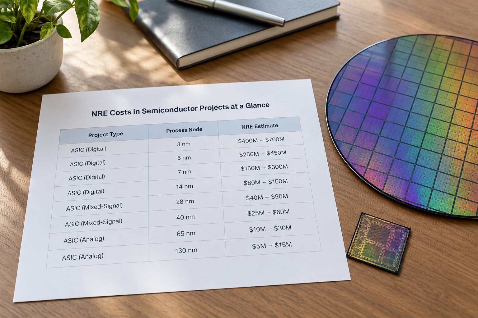
Broad US planning bands for first-of-a-kind chip programs, by project class and process node:
| Project class | Typical process node | First-of-a-kind NRE band | Design effort |
|---|---|---|---|
| Small analog, RF or mixed-signal ASIC | 180nm to 90nm mature | 1M to 5M dollars | Small team, short schedule |
| Structured digital block with qualified IP | 65nm to 28nm | 5M to 15M dollars | Moderate, reuse-heavy |
| Mid-complexity SoC, one tape-out | 40nm to 16nm | 15M to 40M dollars | Large, verification-heavy |
| Leading-edge digital or AI accelerator | 7nm and below | 100M to 250M dollars and up | Very large, multi-year |
| Advanced packaging or chiplet integration | Any node, 2.5D or 3D | Add 10M to 50M dollars on top | Driven by interposer and test work |
The far-right column is where node migration arguments usually collapse. A smaller die does not mean a cheaper program, because mask cost, verification effort, and IP licensing all scale with the process rather than with die area.
How NRE Costs in Semiconductor Projects Are Estimated
There is no reliable public national average for semiconductor NRE, and anyone who quotes you one is guessing. Planners estimate bottom-up instead, starting from an architecture decision and a block list. From there you size the team by discipline and duration, which gives the labor line that usually dominates the budget.
Next you attach the tool and IP assumptions: which EDA licenses are needed for how long, which interface or memory blocks are licensed rather than built, and what the royalty structure looks like after production. Then you count mask layers for the chosen node, add the tape-out and wafer cost for the first lot, and price test, packaging, and qualification.
Finally you spread that across a schedule. Multiply monthly burn by months, add contingency for respin risk, and you have a first-order range rather than a fake precise number. The range, honestly stated, is far more useful to a finance team than a single figure with four significant digits.
What Is Included in Semiconductor NRE?
The definition snippet people search for, stated plainly: semiconductor NRE covers every one-time cost incurred between product concept and volume production, including design labor, EDA and IP licensing, mask sets and tape-out, silicon bring-up, test development, packaging qualification, and compliance documentation. Here is how that breaks down into line items.
- Architecture and specification. Requirements, block partitioning, register maps, and the decisions that fix the rest of the design. Cheap per month, expensive to get wrong.
- RTL design and design services. The engineering hours that turn the architecture into logic and layout, whether done in-house or bought from a design services firm.
- Verification and sign-off. Simulation, formal checks, emulation, and the physical sign-off flow. Frequently under-budgeted on first programs.
- EDA tool licenses. Digital, analog/mixed-signal, physical design, and analysis seats, priced per engineer per year.
- IP licensing and royalties. SerDes, DDR controllers, PCIe, MIPI, and hard macro or standard-cell licenses. Royalties continue per unit and are not NRE.
- Mask sets and tape-out. Reticle fabrication for every layer, plus the mask prep and wafer starts for the first lot.
- Silicon bring-up. Lab bring-up, characterization, debug, and any respin. Model this as likely, not possible.
- Test, packaging, and qualification. Test program development, probe and final test engineering, package design and assembly development, plus reliability and JEDEC or AEC-Q100 qualification work where required.
Everything above stops when volume production begins, with two exceptions worth noting. IP royalties and mask set reuse can carry into the production phase, and some requalification work returns later if the process or package changes.
What Affects Semiconductor Project NRE?
The first driver is design complexity. A block count alone tells you little, but a design with wide analog interfaces, mixed signal, or unusual memory topology reliably runs heavier verification and more iterations than a clean digital pipeline.
Process node comes next. Moving from a mature node to a leading-edge node adds mask layers, multi-patterning, more expensive EDA flows, and a much steeper learning curve for the team. The industry cost ladder that analysts cite puts from-scratch design cost at roughly 40M dollars around 28nm, about 106M dollars at 16nm, roughly 249M dollars at 7nm, and near 449M dollars at 3nm. Those are full custom-program figures, not single-block costs, and they scale down for derivative designs that reuse an existing platform.
Mask economics amplify the node effect. A reticle is written per layer, and industry commentary commonly cites a write-off of roughly 50,000 dollars when a mask turns out to be defective, which is why early mask inspection pays for itself. More layers also means more chances to absorb that cost.
Team duration is the quiet multiplier. Schedules slip at verification and bring-up, and every extra month carries fully loaded engineering cost even when no new tools are bought. EETimes has cited a 32nm device design cost around 75M dollars plus roughly 12M dollars of additional NRE, a good illustration of how a second phase gets appended to the original scope.
Packaging and qualification round out the list. Automotive-grade parts carry extra reliability and qualification budgets that consumer parts skip entirely, and chiplet work adds interposer, known-good-die, and advanced test costs that are frequently missing from early budgets.
Cost Differences by Process Node
Design cost and mask cost both climb steeply as the node shrinks, which is why the same architecture costs wildly different amounts to implement at different nodes:
| Node | From-scratch design cost (IBS ladder) | Mask and tape-out profile | Who should consider it |
|---|---|---|---|
| 180nm to 130nm | Well under 10M dollars | Few layers, inexpensive masks, mature IP | Analog, power, sensor and cost-driven designs |
| 65nm to 28nm | Roughly 40M dollars at 28nm | Dozens of layers, moderate mask cost | Most commercial SoC and ASIC programs |
| 16nm | About 106M dollars | More layers, tougher design rules | Performance-driven products with real volume |
| 7nm | About 249M dollars | Layer count and patterning push masks higher | Large companies and funded startups with high volume |
| 3nm and below | Near 449M dollars | Highest mask and EDA burden in the industry | Very few programs |
Two refinements matter in practice. First, the ladder describes a from-scratch design, and a derivative chip built on a proven platform can land a fraction of it. Second, a mature node with analog content can cost more than a simple design at 16nm, because analog layout does not shrink the way digital logic does.
How to Build a Project-Level NRE Budget
Build the budget line by line, keep the ranges, and make every assumption visible so a reviewer can argue with the assumptions instead of the total.
- Write the architecture scope first. List every block, who builds it, and which parts are licensed. Scope drift after this point is the most common cause of overrun.
- Size the team and the schedule. Fully loaded monthly cost per engineer multiplied by headcount and months, including the months for verification, bring-up, and test development.
- Price the tools and the IP. EDA seats by discipline and duration. IP either as a one-time license fee or a per-unit royalty, and be explicit about which one applies.
- Price masks and the first wafer lot. One mask per layer, plus a multi-project wafer shuttle run if volume justifies it instead of a dedicated set.
- Add test, packaging, and qualification. Test program development, package and substrate engineering, assembly development, and reliability testing.
- Set contingency and a respin reserve. Engineers on r/ASIC describe real 5nm and 7nm numbers as unguessable under NDA, which is why the contingency line is not optional.
- Model amortization last. Divide total NRE by the volume you actually commit to, not the volume you hope for.
A worked example makes the shape clear. Suppose a mid-complexity mixed-signal SoC on a mature-to-mid node carries 12M dollars of NRE across an 18-month program, and the resulting part carries 3.50 dollars of recurring wafer, package, and test cost. The alternative is an FPGA-based solution at 40 dollars a part with no upfront spend.
The break-even calculation is simple: NRE divided by the per-part saving. Here that is 12,000,000 dollars divided by the 36.50 dollar gap between the FPGA and the ASIC, which lands near 329,000 parts. Below that volume, the FPGA wins on total cost. Above it, the ASIC wins, and the margin keeps widening because the ASIC per-part cost never moves.
At 10,000 parts a year, this design adds about 3 dollars of amortized NRE to every part. At 100,000 parts a year, it adds roughly 1.20 dollars. That single table of volumes is what a finance partner actually wants to see.
Ways to Save Without Creating Production Risk
Cutting NRE is mostly about avoiding rework and choosing the right starting point, not about cutting engineers.
- Pick the node the volume can support. Moving one node up rarely pays back at low volume. Stay on a mature or specialty node unless performance or power genuinely requires the move.
- Reuse qualified IP and prior platforms. A derivative of a design already taped out avoids most architecture, verification, and mask cost. This is the single largest lever available.
- Stage the path: FPGA, then small ASIC, then advanced node. Practitioners on Hacker News describe exactly this sequence as a way to keep NRE aligned with what the volume can support.
- Use a multi-project wafer for the first lot. Shuttle runs share mask cost with other designs, which suits early evaluation and low-volume builds.
- Budget verification properly from day one. Cutting simulation and emulation hours moves cost into bring-up, where it is harder to control.
- Stage tape-outs. A full-function first release plus a small later increment can avoid a full re-spin when requirements shift.
- Freeze the package early. Late package changes force new substrates, new test programs, and often a second qualification cycle.
- Agree mask ownership and reuse rights in writing. Confusing mask custody is a common dispute when a derivative product needs the same set.
One caution: quoted prices are typical US ranges that shift with node capacity, foundry terms, and market conditions. Recheck every band against current vendor quotes before committing.
Frequently Asked Questions
Is there a standard national average for semiconductor NRE?
No. There is no published national average, because almost every real figure sits behind an NDA and projects differ too much to average meaningfully. Analysts publish design-cost ladders by process node instead. Use those as order-of-magnitude bands and build your own budget bottom-up from team, tools, IP, masks, test, and packaging.
Does semiconductor NRE include masks, IP, EDA tools, and packaging?
Usually yes, but the boundary varies by contract. Mask sets, tape-out, EDA licenses, IP license fees, test development, and package development are normally NRE. Ongoing IP royalties, wafer cost, package assembly, and final test are recurring per-part costs. Always ask which line a quote puts each item on before comparing two proposals.
Why does a leading-edge chip cost more to design than a mature-node chip?
Because the work scales with the process, not the die. Leading-edge nodes add mask layers, patterning steps, tougher design rules, costlier EDA flows, and longer debug cycles. Industry cost ladders put from-scratch design cost near 40M dollars at 28nm and near 449M dollars at 3nm. Analog-heavy designs are an exception, since analog layout scales poorly with node shrink.
Can an FPGA prototype reduce the NRE budget for an ASIC project?
Yes, and it is a standard strategy. Validating the design on an FPGA first catches logic and interface bugs before mask costs are committed, which reduces bring-up and respin risk. FPGA devices and their tools are recurring per-part costs rather than NRE, so the real saving is in avoided rework and a smaller first program scope.
Which semiconductor expenses are one-time rather than recurring?
Design labor, EDA seats, IP license fees, mask sets, tape-out, silicon bring-up, test program development, package development, and qualification are one-time. Wafer fabrication, substrate and assembly, final test, and IP royalties repeat on every part. Mask sets can become one-time again if you pay for a derivative spin rather than reusing the original set.
How much contingency should a first-time chip project budget for NRE risk?
A first program should carry a meaningful reserve because post-silicon debug and a second tape-out are common rather than exceptional. Teams that budget NRE without a respin reserve are the ones that get surprised, and the overrun usually lands late, when there is no room left in the schedule.
What to Do First
Start by splitting your estimate into two columns: everything that happens once, and everything that happens per part. Most disagreements between vendors come from mixing those two columns. Once they are separated, pick a node your committed volume supports, write the seven budget line items above, and divide by the volume you will really buy.
Figures in this guide are typical US planning ranges that vary by region, node, and foundry and change over time. Confirm every band against current quotes before a budget goes to a steering committee.