SRAM stores a bit in a six-transistor bistable latch, DRAM stores it as charge on a single capacitor. That one physical difference decides everything else: SRAM is fast and expensive per bit, DRAM is dense and cheap per bit but needs periodic refresh. Here is how each cell actually works inside the chip.
Understanding SRAM vs DRAM and how they differ inside the chip matters more than the textbook one-liner suggests. A cache miss, a refresh conflict, and a row-buffer hit all trace back to the physical layout of two small circuits, and knowing which one sits where in your design saves a lot of guessing later.
Both are volatile, by the way. Neither keeps data once power is removed, which is where they part company with flash, FRAM and MRAM. If you have heard that DRAM is non-volatile, that is the single most common misconception in this corner of computer architecture.
Table of Contents
- SRAM vs DRAM How They Differ Inside the Chip at a Glance
- What Is SRAM?
- What Is DRAM?
- How SRAM and DRAM Store a Bit
- How a read happens in SRAM
- How a read happens in DRAM
- Speed and Access Time
- Density and Physical Size
- Power Consumption and Data Retention
- SRAM vs DRAM in Modern Chip Architectures
- Which Should You Choose?
- Frequently Asked Questions
- Is SRAM faster than DRAM?
- Why does DRAM need a refresh operation?
- Can SRAM be used as main memory?
- Why is SRAM more expensive than DRAM?
- Does DRAM retain data when the chip is powered off?
- Can a chip use both SRAM and DRAM?
- Conclusion
SRAM vs DRAM How They Differ Inside the Chip at a Glance
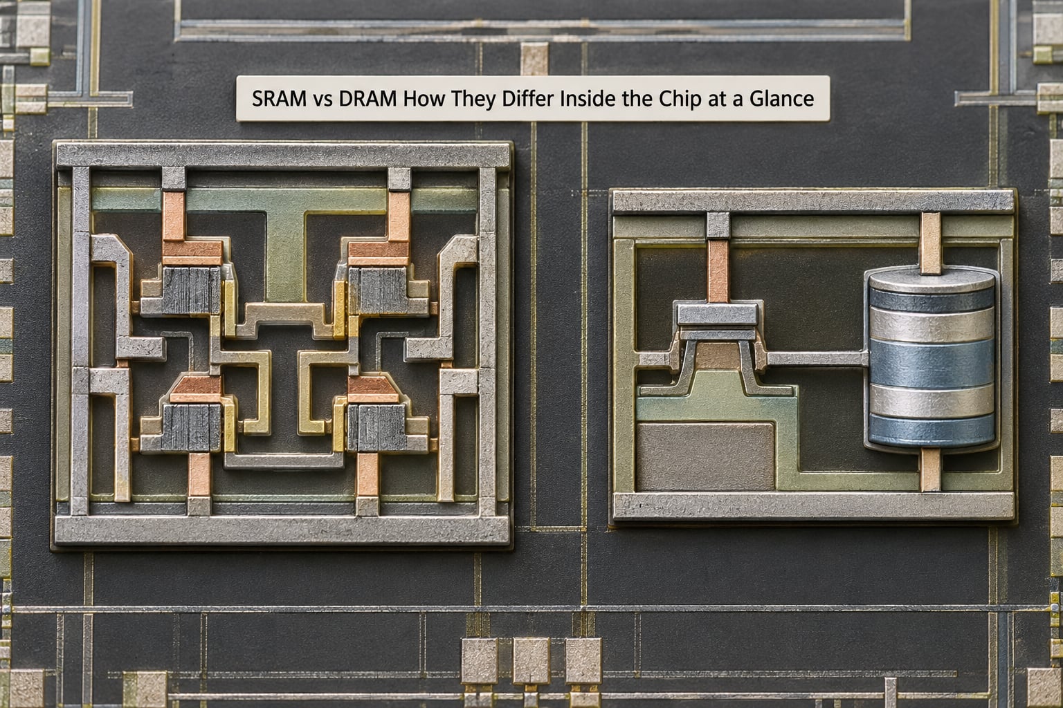
The table below is the short version. Every row traces back to the cell structure, so read it once and then jump to the sections that matter for your design.
| Parameter | SRAM | DRAM |
|---|---|---|
| Cell structure | Six transistors: four latch, two access | One access transistor, one capacitor |
| Storage mechanism | Two cross-coupled inverters hold a state | Charge stored on a capacitor |
| Refresh required | None | Every row re-written within 64 ms |
| Typical cell area | About 120-140 F2 | About 20-30 F2 |
| Access time, typical | 0.5-2.5 ns | 30-70 ns, pattern dependent |
| Row hit versus row miss | No row buffer, access is uniform | Row hit roughly 25-30 ns, row miss roughly 50-70 ns |
| Latency character | Deterministic, near-zero wait states | Command sequence, variable by access pattern |
| Max density per die | Roughly 1-4 Gbit | Roughly 16-32 Gbit |
| Operating voltage | Around 1.8 V in discrete parts | About 1.1-1.2 V for DDR5 |
| Active power profile | Switching plus leakage at full speed | Burst transfers plus a refresh overhead |
| Standby power profile | Leakage dominated, scales with area | Refresh continues whether or not you read |
| Cost per bit | High, tied directly to die area | Low |
| Controller complexity | Simple: chip enable, output enable, write enable | State machine: bank scheduling, refresh, burst, ECC |
| Typical use | L1/L2/L3 cache, register file, scratchpad, block RAM | Main memory: DDR5, LPDDR5, GDDR, HBM |
What Is SRAM?
SRAM stands for static random-access memory. Static means the stored state stays put as long as power is applied, not that it is fixed or permanent.
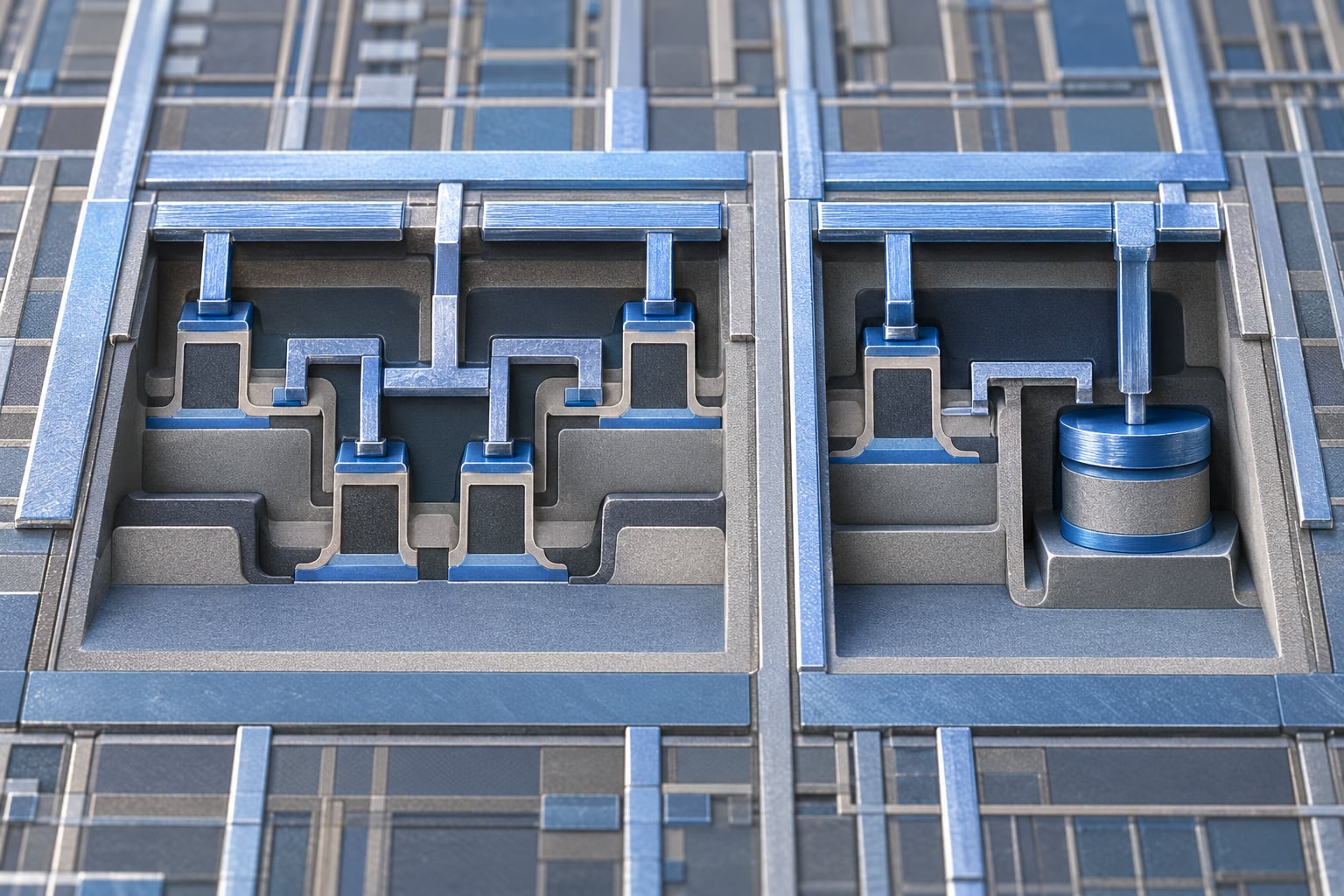
Each bit lives in a six-transistor cell, usually called the 6T cell. Four transistors form two cross-coupled CMOS inverters, and the pair is bistable: it sits at one of two valid states and stays there with no help from outside. The remaining two transistors are access devices that connect the latch to the bitlines when a wordline is asserted.
The forum question that comes up most often is whether SRAM is just an array of flip-flops. It is closely related, and the practical mental model is that SRAM is a memory array built out of the same latch circuitry already used inside a processor. The difference is purpose: a flip-flop is a state-holding element wired into a data path, while an SRAM cell is optimised for regular, addressable array access with predictable wordline and bitline timing.
The register file in a CPU core is a small SRAM-like structure built from latches, and it feeds the execution units. L1, L2 and L3 caches, scratchpad memories, microcontroller internal SRAM and FPGA block RAM are all the same idea at larger scale.
What Is DRAM?
DRAM stands for dynamic random-access memory. Dynamic means the stored value fades, so a controller has to put it back.
Each bit uses a single access transistor and a single capacitor, the 1T1C cell. Charge on the capacitor represents a one, no charge represents a zero. The transistor connects the capacitor to a bitline only when the wordline for its row is asserted, which is why DRAM needs a whole row activated before any single bit can be read.
JEDEC specifies that every row must be rewritten at least once every 64 milliseconds, and the refresh rate rises with temperature. The memory controller schedules those refreshes around normal traffic, so a refresh can steal cycles from a burst you were waiting on.
Density comes from the cell itself. A modern DRAM die carries 16 to 32 Gbit, while a discrete SRAM part tops out around 1 to 4 Gbit, because six transistors per bit takes roughly five times the silicon area of a transistor and a capacitor.
How SRAM and DRAM Store a Bit
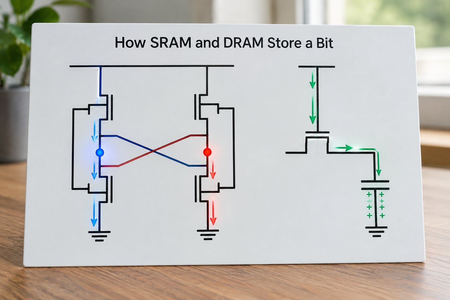
The two mechanisms look different on a layout and behave differently in silicon, so it helps to walk a read through each.
How a read happens in SRAM
- The bitline pair is precharged to a known mid-level voltage before the access begins.
- The wordline for the target row goes high, turning on both access transistors.
- The latch drives one bitline up and the other down, creating a small differential.
- A sense amplifier resolves the differential, and the latch value is restored across the cell automatically.
No restoration step is needed because the cell regenerates its own state from supply the whole time it is held. That is why SRAM read latency is so short and why it does not vary with what you read before it.
How a read happens in DRAM
- An ACTIVATE command opens a row, connecting every cell in that row to its bitline and latching the sense amplifiers.
- A READ command streams a burst of columns out of that open row through the same sense amplifiers.
- A PRECHARGE command closes the row and returns the bitlines to their precharged state, ready for the next row.
While the row sits open in the row buffer, further reads to the same row are cheap. Reading a different row means a precharge, a second ACTIVATE and a wait for tRC, which is where the gap between a row hit and a row miss comes from. The capacitor also gets read destructively, since the charge-sharing that produces the bitline voltage empties the cell, so the sense amplifier has to write the value back before the row closes.
Speed and Access Time
SRAM is faster than DRAM, and the reason is the number of steps a read requires. SRAM needs a precharge, a wordline pulse and a sense resolve, with no row protocol in between. DRAM needs a command sequence, a row to be open, and a refresh schedule running in the background.
Is SRAM faster in practice? It wins on latency. SRAM access sits in the 0.5 to 2.5 ns range, while a DRAM access spans roughly 30 to 70 ns depending entirely on the access pattern: a row hit lands near 25-30 ns and a row miss pushes toward 50-70 ns. Sequential streaming, though, plays to DRAM’s strengths, and a wide interface can deliver far more bytes per second than any on-die SRAM of comparable cost.
That is why a cache exists at all. With average memory latency t_hit plus the miss rate times the miss penalty, any non-zero miss rate lands on DRAM’s timing, and no amount of faster logic on the core side hides it. Caches are sized to push that miss rate down, not to make memory itself quicker.
Density and Physical Size
Density is where the cell-structure difference becomes financial. An SRAM cell occupies roughly 120-140 F2, where F2 is the minimum-feature area of the process node, against roughly 20-30 F2 for a DRAM cell.
Multiply that ratio by the billions of bits a main memory needs and the outcome is not a small optimisation, it is the difference between a chip you can build and a chip you cannot. Because silicon area is cost, the same ratio shows up in cost per bit, in die size, and in how much cache a given core budget can afford.
DRAM also has a scaling advantage in a way SRAM does not. The 6T latch is remarkably durable, which is why it has stayed at six transistors for decades despite every other circuit on the die shrinking, but it cannot shrink below what the six devices and their spacing physically require. DRAM cells, by contrast, keep gaining density through process and capacitor improvements while the cell logic stays simple.
Power Consumption and Data Retention
SRAM spends power on leakage, DRAM spends power on refresh, and the crossover depends on how long a bit sits untouched.
A static cell holds its state with no switching activity, so a block that is written once and read rarely costs almost nothing. The cost that never goes away is subthreshold leakage, which scales with cell area, so a large idle SRAM array is the leakiest thing on a modern chip. A dynamic cell that is refreshed but never read burns refresh power indefinitely, and the refresh tax grows with temperature because leakage speeds up.
Operating voltage follows from the same physics, sort of: DRAM arrays run near 1.1-1.2 V in a DDR5 interface, while discrete SRAM parts are commonly specified around 1.8 V. Both technologies are volatile, meaning contents are lost when power is removed. That is the difference from flash, FRAM and MRAM, which keep data without power.
SRAM vs DRAM in Modern Chip Architectures
Almost every modern chip contains both, placed by the memory hierarchy according to speed and cost.
- Register file and L1/L2/L3 cache: SRAM, sized in tens of megabits, accessed within a couple of nanoseconds.
- Scratchpad and tightly coupled memory: SRAM, deterministic and core-local, used where software must guarantee a known access time.
- FPGA block RAM: SRAM, commonly tens of megabits per block, which is often the constraint that forces an external DRAM part into the board design.
- SoC shared SRAM and tightly coupled on-chip buffers: SRAM, sized down until die area starts hurting yield.
- Main system memory: DRAM, on DDR5, LPDDR5, GDDR and HBM interfaces, where capacity dominates and the memory controller is a substantial block of logic in its own right.
DRAM, LPDDR, GDDR and HBM are interface families of the same underlying technology, not different kinds of memory cell. They differ in power envelope, pin architecture and how they are stacked, not in how a bit is stored.
Why can DRAM not simply serve as cache? Because the controllers are not interchangeable. A discrete SRAM interface is chip enable, output enable and write enable, and reading a word is one operation. A DRAM controller runs a state machine that tracks which rows are open in which banks, schedules refresh, bursts data out in time with the data-strobe protocol, and usually handles ECC. The overhead is not in the memory array, it is in the sequencing logic, and that logic is exactly what a cache access cannot afford.
Which Should You Choose?
Start from the required capacity, then work backwards to speed, because capacity is what forces the expensive decision.
- Choose SRAM when the working set is small and access time must be predictable: register files, caches, scratchpads, FPGA buffers, tightly coupled memory, and microcontroller internal RAM.
- Choose DRAM when the working set is large and streaming is acceptable: main memory, frame buffers, packet buffers, and AI accelerator working memory on HBM.
- Choose both when the access pattern is mixed. A small SRAM scratchpad that absorbs the hot working set often removes the need for a much larger, faster DRAM interface.
Two practical checks save rework. If the design is bandwidth-bound, compare sustained transfer rates rather than access times, because that is where DRAM can win. If the design is latency-bound or power-sensitive while idle, check the leakage cost of the SRAM area you just added, since idle leakage scales with every cell you place.
Frequently Asked Questions
Is SRAM faster than DRAM?
Yes for latency, not always for throughput. SRAM access takes roughly 0.5-2.5 ns with no row protocol, while a DRAM read runs 30-70 ns depending on whether the row is already open. A wide DRAM interface, however, streams far more bytes per second in a burst, which is why bandwidth-bound designs often still prefer DRAM.
Why does DRAM need a refresh operation?
Because a DRAM cell stores its value as charge on a capacitor, and that charge leaks away through the access transistor and the capacitor dielectric. The stored voltage eventually falls below the sense amplifier’s read threshold, so the controller re-reads and rewrites every row at least once every 64 milliseconds. Higher temperatures shorten retention, so the refresh rate goes up as the chip gets hot.
Can SRAM be used as main memory?
Technically yes, but it is rarely a good idea. A 16 GB main memory built from six-transistor cells would need on the order of a thousand times the silicon area of a DRAM version, and the cost and yield would be prohibitive. SRAM does serve as main memory in very small systems, such as some microcontrollers, where capacity needs are tiny.
Why is SRAM more expensive than DRAM?
It comes down to die area. An SRAM cell needs about 120-140 F2 against roughly 20-30 F2 for a DRAM cell, and silicon area is the main driver of chip cost. Since the same die budget spent on DRAM yields many more bits, the cost per bit gap is large, typically hundreds of times for the same capacity.
Does DRAM retain data when the chip is powered off?
No. DRAM is volatile, and so is SRAM: both lose their contents the moment supply is removed, which is why controllers flush dirty cache lines and write back buffers before shutdown. If you need data to survive power loss, the alternatives are non-volatile technologies such as flash, FRAM or MRAM, not a different flavour of DRAM.
Can a chip use both SRAM and DRAM?
Yes, and most do. A processor SoC places SRAM in the register files and cache hierarchy for nanosecond access, and pairs it with a DRAM controller driving external DDR5, LPDDR5, GDDR or HBM for capacity. Embedded designs follow the same pattern with on-chip block RAM backed by an external DRAM part.
Conclusion
SRAM vs DRAM is one decision, made at the cell: hold the bit in a six-transistor latch, or hold it as charge on a capacitor. The latch gives deterministic nanosecond access and no refresh; the capacitor gives roughly five times better density and a far lower cost per bit, at the price of a refresh schedule and a command sequence on every access.
Before choosing anything, write down the capacity you need and the worst-case latency you can tolerate. Capacity forces the SRAM-versus-DRAM call, and everything else in the design, from cache sizing to whether you need an external memory interface, follows from that pair of numbers.