3D NAND architecture is a flash memory design that stacks non-volatile memory cells vertically, dozens to hundreds of layers deep, above a single CMOS die. Instead of shrinking the cell in two dimensions, manufacturers add layers, so density rises while the process node stays relatively large. That single idea is why nearly every SSD, phone and memory card you can buy today is built this way.
This guide walks the structure from a single cell up to the controller that talks to your host, then covers how the array is built, why stacks of 300 layers and more are difficult, and what a controller does about errors that planar flash never had.
Table of Contents
- What Is 3D NAND Architecture?
- How 3D NAND Stores Data in Vertical Layers
- The Main Building Blocks: Pages, Blocks, Planes, and Dies
- The Array and Its Periphery: NAND Flash, Channels, and Logic
- How 3D NAND Architecture Is Manufactured
- How Data Moves Through a 3D NAND Device
- Why 3D NAND Architecture Uses So Many Control Lines
- Types of 3D NAND Architectures and How They Differ
- How 3D NAND Architecture Affects Performance and Endurance
- Frequently Asked Questions
- How does 3D NAND work?
- What is the difference between NAND and 3D NAND?
- What are the disadvantages of 3D NAND?
- Is 3D NAND any good?
- How many layers do modern 3D NAND chips have?
- Why does 3D NAND use charge trap instead of floating gate?
- Conclusion: Start With the Vertical Memory Array
What Is 3D NAND Architecture?
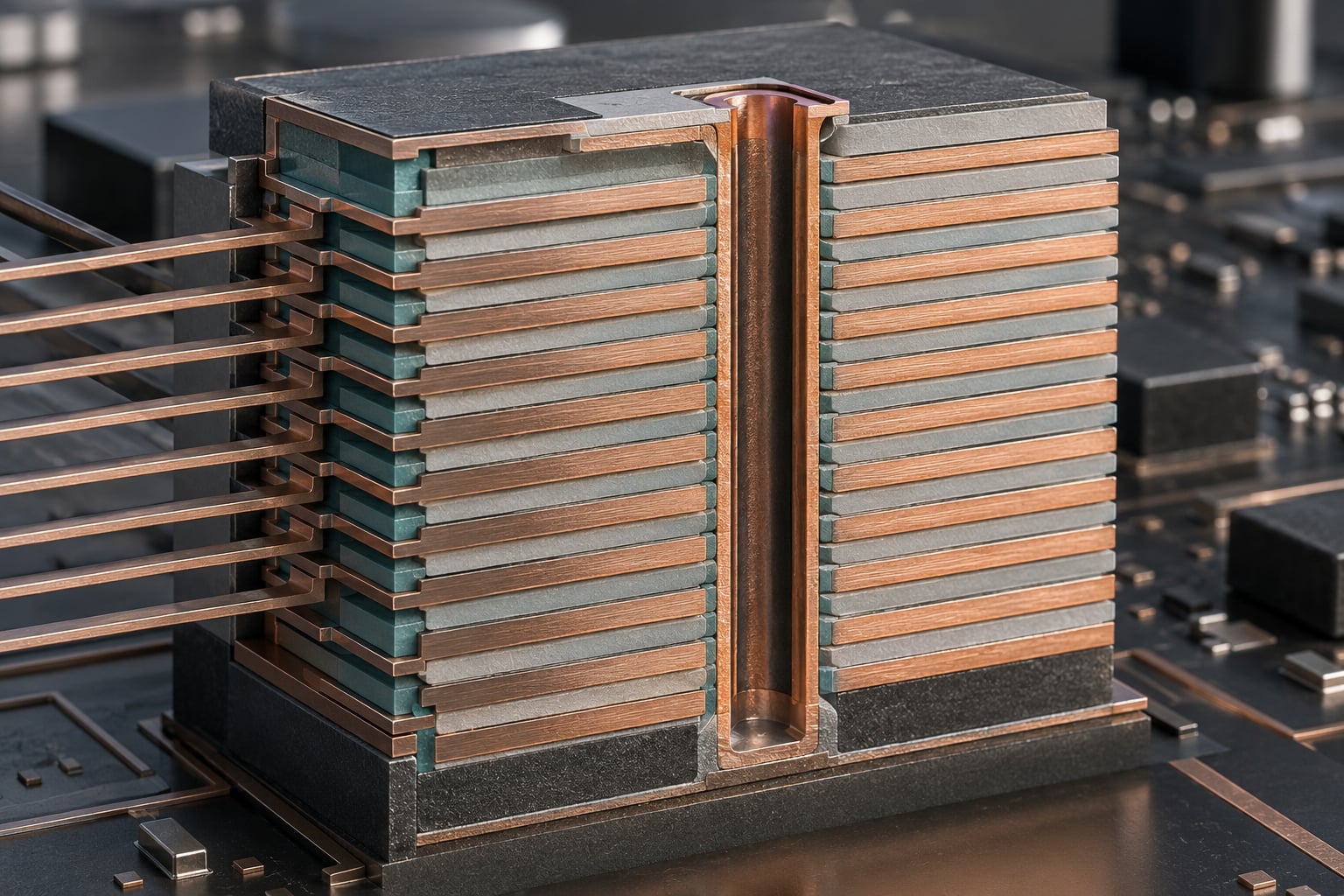
3D NAND architecture means a flash memory array in which transistors are deposited in layers stacked vertically over a logic base, connected by vertical channel holes, and addressed by word lines running horizontally through the stack. NAND here is the same non-volatile flash family as before; “3D” describes the geometry, not a new memory principle.
The reason for the geometry is economic. Planar flash scaled by making cells smaller in the wafer plane, and by the mid-2000s that route was fighting lithography limits, mask counts and yield. Stacking moved the effort into deposition and etching instead, which is what the industry calls bit cost scaling.
It helps to separate 3D NAND from the other memories people lump it in with. DRAM is volatile and accessed by address, one bit at a time, so it loses contents at power-off. 3D DRAM, in development at several labs, stacks DRAM cells vertically but keeps that one-bit-per-address model. NOR flash, by contrast, allows random access to any cell and is used for code storage, not capacity. 3D NAND is non-volatile, page-addressed, and read in long strings.
The comparison below covers the differences that actually drive design choices. Note the cell type row: SLC, MLC, TLC and QLC describe bits per cell, which is independent of the array being planar or 3D.
| Characteristic | 2D (planar) NAND | 3D NAND |
|---|---|---|
| Cell placement | Flat, in the wafer plane | Vertical layers above the CMOS logic |
| Density growth | Lateral shrink plus multi-patterning | More layers per die |
| Process node in production | Frozen near the 30 nm era | Around 40 nm and stable for years |
| Dominant cost driver | Lithography and mask count | Deposition, etch steps, stack height |
| Charge storage | Floating gate mostly | Charge trap almost universally |
| Channel | Planar transistor channel | Vertical hole filled with polysilicon |
| String length | Tens of cells | Often 100 to 300+ cells per string |
| Cell types available | SLC through QLC | SLC through QLC, same definitions |
| Error behaviour | Cell-to-cell variation | Cell-to-cell plus layer-to-layer variation |
| Typical use | Effectively discontinued | SSDs, phones, cards, data centers |
How 3D NAND Stores Data in Vertical Layers
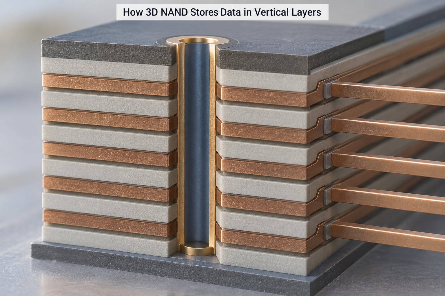
Each cell in the array is a charge trap transistor. Electrons tunnel through a thin tunnel dielectric into a thin band of silicon nitride trapped between two insulators, and the amount of charge shifts the cell’s threshold voltage. The controller reads the bit by applying a reference voltage on the word line and asking whether the cell conducts.
The classic alternative, the floating gate, uses a conductive polysilicon island that electrons tunnel onto and off. In a vertical stack, the floating gate is a cylinder lining the channel hole. Scaling the nitride trap instead means the charge sits in a thin band rather than a thicker conductor, so two cells can be packed closer and programmed with lower voltages.
Stack height buys density for a simple reason: a taller stack means more bits per unit of wafer area without asking the lithography tools to print a smaller feature. Taper, though, is the catch. A channel hole that is straight gives every cell the same gate length. A hole etched to a slight angle gives the top cells a longer channel than the bottom ones, so the etch process is designed to keep the taper angle very small.
Another detail worth knowing: the channel is a physical stack of transistors in series. A string of 200 cells means current must pass through 200 channel regions to reach the sense amplifier at the bottom. That is why a single bad cell can affect a whole string, and why read and program operations are defined for groups rather than single bits.
The Main Building Blocks: Pages, Blocks, Planes, and Dies
Memory designers talk about 3D NAND in a strict hierarchy, and each level has a different role in program, read and erase.
Cell is the single charge trap transistor. Its state is stored as one or more threshold voltage levels.
Page is the smallest unit that can be programmed or read. Because one word line crosses a whole plane, a page equals the set of cells sharing that word line across every bit line. A read moves this page into the sense amplifiers, and a program pushes a page’s worth of data down in one pass.
Block is the smallest unit that can be erased. It is a set of pages sharing a set of word lines, and in 3D NAND it also spans one layer, because a word line is defined by a single layer at a given height in the stack. Erase happens in about a millisecond per block, program in tens of microseconds per page, so erase is the operation that dominates write cost.
Plane is a group of blocks that share the same bit lines and can be programmed in parallel. Parallel planes raise throughput; a die with four planes is roughly four times faster in sustained writes than an otherwise identical die with one.
Die is one wafer’s array plus its peripheral logic. A package holds several dies stacked with a shared bus, and a controller sits alongside them on the same module.
The Array and Its Periphery: NAND Flash, Channels, and Logic
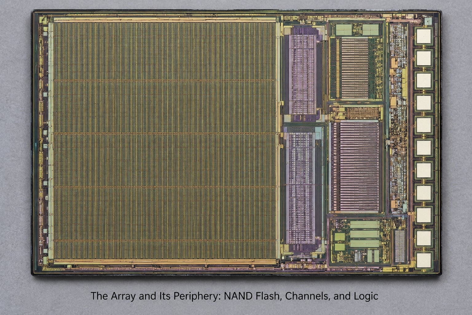
The array itself is only the vertical transistor structure. Everything around it is ordinary CMOS logic, and that logic is what makes the array usable.
Word line drivers sit under the array in the CMOS base, one per word line, and push the program, pass and read voltages onto the stack. Bit lines run vertically along the array edge, and sense amplifiers compare the current in each string against a reference voltage to resolve the stored threshold level. A page cache, usually made of SRAM, sits between them so a whole page can be loaded or held while the array is read or programmed.
Row and column decoders select which word lines and bit lines are active. Charge pumps generate the program and erase voltages, which sit well above the logic supply, and on-die error correction works alongside the controller to keep the raw bit error rate inside what the outer ECC can handle.
This split is a deliberate economic choice. The array uses older, larger, cheaper nodes, often around 40 nm, while the periphery scales on a modern node. The interface between them, usually a high-speed parallel bus, runs much faster than the internal array can read, so the page cache absorbs the mismatch.
How 3D NAND Architecture Is Manufactured
The process builds a layer cake first and carves it afterwards. The order matters, because none of the later steps can fix an early defect.
- Start with the CMOS logic wafer. Peripheral circuits, decoders, drivers and charge pumps are built first using the foundry’s standard process.
- Deposit the alternating stack. Insulator and conductor films are deposited repeatedly, each a few tens of nanometres thick. On some architectures, germanium is introduced into the polysilicon channel layers to raise electron mobility, which is one response to tall stacks.
- Etch the channel holes. This is the defining step. A single lithography pattern is projected and etched through hundreds of layers at once, a high aspect ratio etch that must stay vertical, uniform and defect-free over a depth that can be several micrometres.
- Build the gate stack in the hole. Grow the tunnel dielectric, deposit the charge trap nitride, grow the blocking dielectric. Three of the four walls get a gate; the remaining wall is left as a staircase so neighbouring cells are separated. This is sometimes called a tube within a tube structure.
- Fill and isolate. The hole is filled with polysilicon to form the channel, then a slit etch separates adjacent strings so each can be selected independently.
- Form contacts and wire up. Contacts are made to the word lines and the channel bottoms, metal layers are added, the wafers are thinned, diced and stacked into a multi-die package.
Because the etch is the risky step, most failures trace back to it. Non-uniformity at the top of the stack, a particle that blocks part of a hole, or a slight taper that lengthens the upper gate, all show up later as cells that read wrong or fail sooner than the rest of the die.
How Data Moves Through a 3D NAND Device
Nothing the host sends to a drive reaches the array as an address the flash understands. Host logical block addresses go to the controller, which owns a flash translation layer and translates them into physical page addresses. That translation is the whole point: it hides erase granularity from the host, and it changes constantly as data moves.
A read starts when the controller resolves a logical address to a page, issues a read command with a page address and a set of reference voltages, and the die copies the page into its SRAM cache. The die returns the data, the controller checks it against its own ECC, and only then does the host receive it.
A program pushes a page’s data into the cache, then the die applies a sequence of program pulses to one word line. Each pulse is followed by a verify read, and the loop stops when every cell in the page has reached its target threshold voltage. The pulses are ramped deliberately because overshooting a cell’s threshold damages its oxide, and a page of program pulses is a main source of program interference on neighbouring cells.
An erase applies a block of voltage in one operation, removing charge from every cell in that block. Because erase works per block, updated data cannot simply overwrite itself. The controller writes new data to a free page, marks the old page invalid, and eventually moves live data around to consolidate free space. That is garbage collection, and it is where wear leveling comes in: the controller tracks program and erase counts per block and steers writes toward less-used blocks so the wear is spread across the die.
Dwell time, the gap between a program and the next access to that cell, matters more in 3D than in planar flash because charge loss accelerates at higher temperature. A drive kept in a hot environment for months can lose data that a cold drive keeps indefinitely, which is why controllers track temperature and hot data age.
Why 3D NAND Architecture Uses So Many Control Lines
Every additional layer adds a word line, and every added word line adds capacitance, resistance and timing. The word lines are long, shared gates running the full width of the array, and the bit lines are long wires running the full height. Both act as distributed RC networks.
With 300 word lines, the driver at the far end of a word line sees far more load than the driver at the near end, and signals degrade along the way. The fix is segmented word lines, so a driver is closer to the cells it serves, at the cost of more drivers. Bit lines run the same problem in the other direction, and sense amplifiers placed periodically along them keep the wire length manageable.
Voltage requirements get harder too. Erase needs a strong field across the tunnel dielectric, and every added layer makes it easier for that field to disturb the cell one level down. The channel in series makes it harder still: string current depends on the worst cell in the string, and a long stack of them drives current low enough that the sense amplifier has trouble separating two adjacent threshold levels.
This is why scaling stopped being a simple layer count. Vendors have documented the vanishing string current problem, where worst-case current falls as stacks grow, and much of the last decade of engineering went into channel materials, sense amplifier design and read reference schemes rather than into adding more layers.
Types of 3D NAND Architectures and How They Differ
Two architectural choices separate the major designs: how the channel is formed, and how many gates wrap around it. A single-gate cell surrounds three walls of the hole, with the fourth wall left open as a staircase. A multi-gate cell, sometimes described as gate-all-around, wraps all four walls, giving more capacitive coupling and a stronger read margin at the cost of a harder isolation step.
The vertical channel, pioneered by Toshiba and developed as BiCS FLASH, is the approach every production part uses today. A via-based structure, in which vias are connected between layers rather than a continuous vertical channel, is simpler to etch but suffers badly from etch-induced damage to the layers below, so it has not reached volume production.
Cell type is a separate axis that readers often confuse with the geometry. A planar array can be TLC, and a 300-layer array can be SLC.
| Cell type | Bits per cell | Voltage states | Relative endurance | Typical use |
|---|---|---|---|---|
| SLC | 1 | 2 | Highest | Industrial, automotive |
| MLC | 2 | 4 | High | Legacy, rarely sold |
| TLC | 3 | 8 | Medium | Client SSDs, phones |
| QLC | 4 | 16 | Lowest | Entry drives, cold storage |
More voltage states mean each level sits closer to its neighbour, so a small shift in threshold voltage flips a bit. That shows up directly as a higher raw error rate and a lower program and erase cycle count, and it is why QLC relies on heavier error correction to reach usable capacities.
Vendors differ mostly in process and integration. Samsung’s V-NAND and Kioxia’s BiCS both use vertical channels with charge trap cells, and so do Micron and SK hynix, the latter having developed CBA, a separately connected array architecture where cells are driven from both ends to shorten the string. Solidigm’s 3D NAND, inherited from Intel, is the main production example that kept a floating gate. Exact layer counts and node choices change with each generation, so check the current data sheet rather than a comparison written years ago.
How 3D NAND Architecture Affects Performance and Endurance
Architecture sets the ceiling on everything a drive can do. Deeper stacks mean more planes and more dies per package, which is how bandwidth keeps climbing while cost per bit falls. But the same geometry introduces error behaviour that has no planar equivalent.
| Error type | Cause | What the controller does |
|---|---|---|
| Layer-to-layer variation | Etch and deposition drift across a tall stack, so cells at the top differ from cells at the bottom | Per-layer read reference voltages, adaptive verification |
| Early retention loss | Charge leaking out of freshly programmed cells, worse when hot | Temperature and hot-age tracking, read-before-write refresh |
| Retention interference | Charge from an unprogrammed neighbour in the same page shifting its threshold voltage | Program order and verify schemes tuned per page |
| Program interference | Program pulses on one word line disturbing the next | Verify loops with tightened margins |
| Read disturb | Repeated reads on one word line slightly shifting cells on it | Periodic scrub reads |
| Charge loss from cycling | Oxide damage accumulating with program and erase cycles | Wear leveling, spare capacity, dynamic wear leveling |
Layer-to-layer variation is the one that is genuinely new with the geometry. Because the stack is built bottom to top, any drift in the etch or the deposition accumulates as you go up, and cells at one layer can have a noticeably different threshold voltage distribution from cells at another. Controller algorithms such as ReMAR and LaVAR exist specifically to sense which layer a block came from and adapt read references and garbage collection decisions to it.
There is also a self-recovery effect: a cell that has drifted toward the wrong threshold can partly return after a read pulse, because a fraction of the trapped charge is re-tunneled at a different rate. It is small, and it is temperature dependent, but it means an error rate measured one way does not predict behaviour days later.
On the power side, the array is low voltage, but the periphery runs the modern logic process and the charge pumps fire hard during program and erase. Program and erase current is the bulk of it, which is another reason controllers batch writes rather than issuing them one page at a time.
Frequently Asked Questions
How does 3D NAND work?
3D NAND alternates thin layers of insulator and conductor on a wafer, then etches deep vertical holes through the whole stack. Each hole’s walls are lined with a tunnel dielectric, a charge trap layer and a blocking dielectric, and filled with a polysilicon channel. Horizontal word lines crossing the stack act as control gates. Programming tunnels electrons into the trap to raise the cell’s threshold voltage, and the controller reads each bit by testing whether the cell conducts at a reference voltage.
What is the difference between NAND and 3D NAND?
NAND is the name of the flash architecture, and 3D NAND describes how that architecture is built. Earlier NAND flash arranged cells flat in the wafer plane and gained density by making them smaller. 3D NAND stacks the cells in layers above the CMOS logic and gains density by adding layers instead. Both are non-volatile and page-addressed, so 3D is a change of geometry, not a different kind of memory.
What are the disadvantages of 3D NAND?
The drawbacks come from the stack itself. A high aspect ratio etch through hundreds of layers is hard to keep uniform, and any drift creates layer-to-layer variation. Longer strings reduce worst-case current, which narrows the read margin. Cells programmed to more voltage states, such as QLC, sit closer together and yield more raw errors. A high layer count also means many more blocks to wear level across before capacity is exhausted.
Is 3D NAND any good?
For most uses, yes, and it is effectively the only flash that matters now. Vertical stacking is what kept cost per bit falling after planar scaling stalled, which is why client SSDs, phones, memory cards and data center drives all use it. The trade-offs are real: more raw errors to correct, and cell geometry that is more sensitive to temperature over time. Modern controllers handle both well enough that the density and cost gains dominate.
How many layers do modern 3D NAND chips have?
Layer counts have climbed steadily from the 24 to 32 layer parts that started the transition, through 96 and 128 layer generations, into the 200-plus range, with production parts now well past 300 layers. The number is a marketing headline more than a quality measure, since cell type, plane count, cache size and controller quality matter as much to real performance.
Why does 3D NAND use charge trap instead of floating gate?
A floating gate stores charge on a conductive island, which in a vertical stack is a cylinder lining the channel hole. A charge trap stores it in a thin band of silicon nitride between two insulators. The trap version is faster to program, uses lower voltages, and scales more predictably as cells get closer together, because a thin band of charge is easier to place precisely than a growing conductor. That is why nearly all production 3D NAND is charge trap today.
Conclusion: Start With the Vertical Memory Array
If you take one idea away from this guide, take this: 3D NAND architecture buys density by building up instead of in, and every other property of the part follows from that geometry. The stack, the vertical channel and the word lines determine density, the string determines read margin, the etch determines uniformity, and the cell type determines how much error correction has to do.
A good order to learn it in is cell, then page, block, plane and die, then the peripheral logic, then the controller’s garbage collection and wear levelling. Get those six levels straight and the datasheet numbers and forum arguments make sense on their own. If you are weighing flash for a design, look at the cell type and the controller’s error correction budget before you look at layer counts.