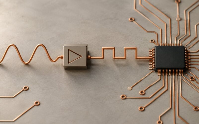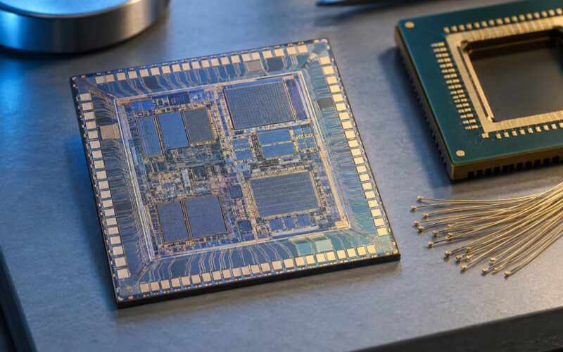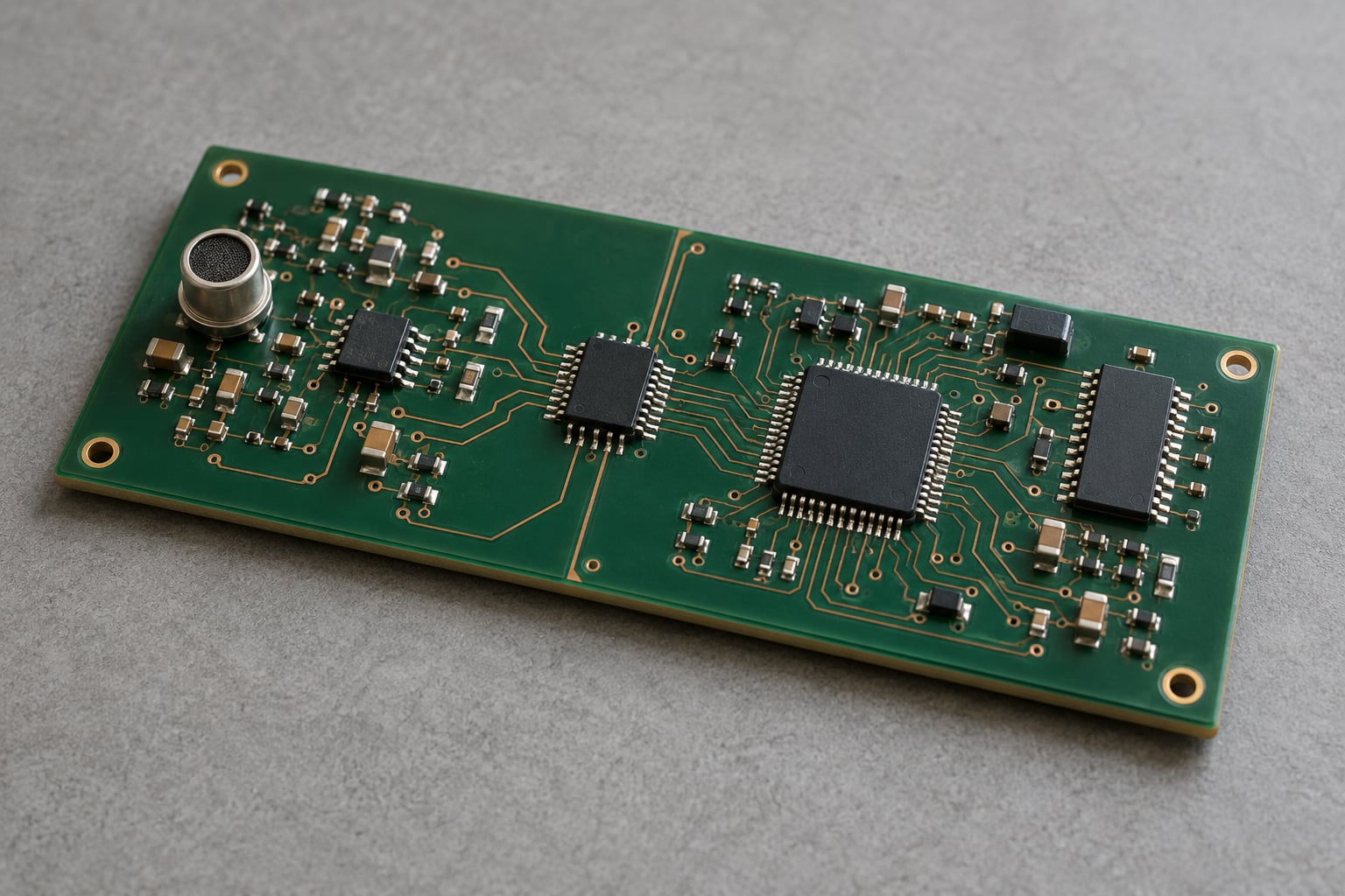
Mixed-signal design is the engineering discipline of putting analog and digital circuitry on the same chip or the same printed circuit board, so a digital processor can capture, interpret, and control the continuous physical world around it. Light, sound, pressure, temperature and radio waves all arrive as analog signals; microcontrollers, memory and logic want discrete binary data. Mixed-signal design is the work of bridging the two, and doing it without letting one domain wreck the other.
That last part is where most of the difficulty sits. A digital block is happy to slam 40 mA through a supply rail in 200 picoseconds; a nearby sensor amplifier wants microvolts of noise. The engineering is not the conversion itself, it is everything required to make the conversion trustworthy.
Below is the working definition, the signal chain, the blocks that show up in almost every design, the applications, and the flow an engineer actually follows. It is written for someone who already knows what a resistor does and wants to know how the two domains are made to live together.
Table of Contents
- How Mixed Signal Design Works
- How it differs from pure analog and pure digital design
- Analog and Digital Signals in One Circuit
- Common Mixed Signal Blocks
- Why Engineers Choose Mixed Signal Design
- ASIC, mixed-signal FPGA, or PSoC
- Where Mixed Signal ICs Are Used
- How a Mixed Signal Design Is Built
- What a mixed signal design actually measures
- What Mixed Signal Design Is Used For
- Frequently Asked Questions
- Can you give me an example of a mixed-signal circuit?
- What is the difference between mixed-signal design and analog design?
- What is AMS in VLSI?
- Can analog signals be replaced with digital processing?
- What are the main challenges of mixed-signal design?
- How do engineers verify a mixed-signal design?
- Conclusion
How Mixed Signal Design Works
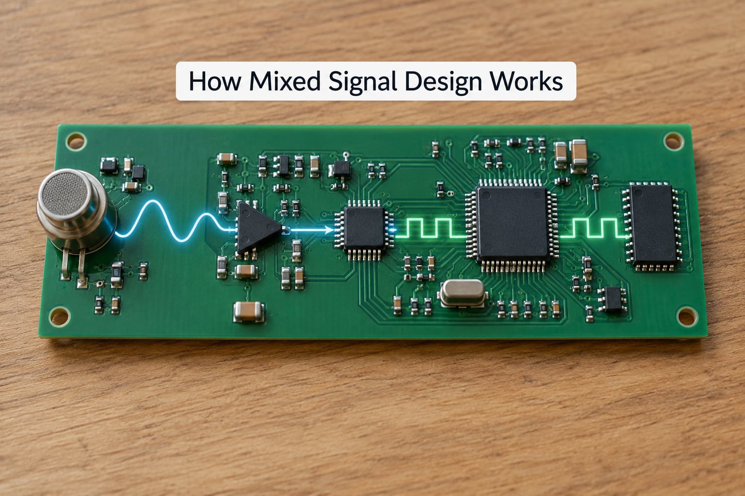
The short version: a mixed-signal design combines analog circuits, which handle continuous real-world physical signals, with digital circuits, which process discrete binary values, on a single integrated circuit die or PCB. The analog side conditions the incoming signal, an analog-to-digital converter turns it into numbers, the digital side computes and decides, and a digital-to-analog converter turns the result back into a voltage, current or drive signal when the world needs an analog answer.
Why combine them at all? Because separating the domains physically costs you something real. An off-chip sensor feeding a board-level converter has to survive connector loss, board capacitance, ground bounce and EMI before the number is even trustworthy. Integrating the front end next to the converter removes most of that path and buys accuracy, lower power and a smaller bill of materials.
It also lets one die do things neither domain does well alone. A microcontroller cannot measure temperature. An op-amp cannot run a control loop across 10,000 measurements a second. Put a converter, a reference and a small processor on one die and you get a smart sensor that calibrates itself, filters its own data and reports in digital form over I2C or SPI.
How it differs from pure analog and pure digital design
Pure analog design deals in continuous quantities and its performance lives in noise, offset, drift, bandwidth and linearity. It is verified by looking at waveforms and spectra on an instrument.
Pure digital design deals in logic states and timing closure, and its verification is largely simulation plus static checks against an RTL description. It scales because a digital tool can synthesize and place millions of identical gates without understanding what any one of them does physically.
Mixed-signal verification is the third thing, and it is often confused with mixed-signal design itself. Verification is how you prove the design meets spec; mixed-signal design is the design itself. AMS verification, meaning analog and mixed-signal verification, is a specific sub-discipline and a genuinely hard one, which is why it gets its own section below.
Analog and Digital Signals in One Circuit
An analog signal varies continuously in time and amplitude. A thermistor’s resistance, a microphone’s millivolt output, the slow droop of a battery’s voltage while it drains: all continuous, all carrying information in the exact value rather than in a state.
A digital signal takes discrete values and carries information in the pattern of those values. A 16-bit ADC output is a number between 0 and 65535. It represents a voltage, but the voltage itself no longer varies continuously on the wire.
Because real inputs are ugly, a raw sensor signal almost never goes straight into a converter. It arrives with a large common-mode offset, a slow drift, interference from adjacent channels, a source impedance that loads whatever you attach to it, and a level that might be 3 millivolts or 3 volts. The analog front end exists to fix all of that before conversion.
A typical chain, drawn as text because the shape matters more than the styling:
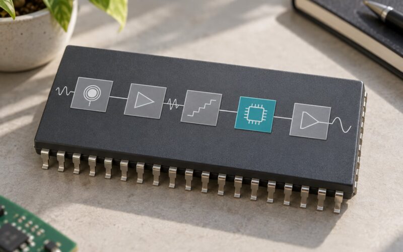
Sensor → protection and filtering → amplifier or instrumentation stage → filter → ADC → MCU, DSP or FPGA → DAC → output driver
Two details decide whether that chain is accurate. First, source impedance: a sensor with 50 kΩ of output resistance feeding a 1 MΩ input divides the signal by 20 before you convert anything. Second, the reference voltage, because an ADC’s code is really a ratio of input to reference, and a reference that drifts 0.1% turns every measurement into a 0.1% error.
Some designs go the other way and mix both directions at once. A battery management part reads cell voltage through an analog front end and ADC, then switches a load with a digital-controlled analog FET driver. That is a mixed-signal path even though the DAC is missing.
Common Mixed Signal Blocks
Almost every mixed-signal design is assembled from the same small set of blocks. The names change between vendors; the jobs do not.
| Block | Role | Spec to watch |
|---|---|---|
| Sensor or transducer | Turns a physical quantity into a voltage or current | Output range, source impedance, noise density, self-heating |
| Operational amplifier | Buffers, gains and levels the input without loading it | Input bias current, offset and drift, noise, GBW, output swing |
| Filter | Removes out-of-band noise and alias content | Corner frequency, stopband rejection, settling time |
| Voltage reference | Sets the scale that every measurement is relative to | Initial accuracy, temperature drift, noise, PSRR, load regulation |
| ADC | Converts an analog voltage into a digital code | Resolution, SNR, ENOB, INL/DNL, input range, sampling rate |
| DAC | Converts a digital code back into a voltage or current | Resolution, settling time, glitch energy, monotonicity |
| Digital control logic | Sequences converters, applies calibration, handles the interface | Clock rate, interface protocol, metastability margin |
| Clock and PLL | Generates the sampling clock and derives other frequencies | Phase noise, jitter, reference feedthrough, lock time |
| Output driver | Delivers power or current to the outside world | RDS(on), current limit, slew rate, thermal pad |
A few of these deserve more than a table row. A fully differential amplifier carries the signal on two opposite-phase lines, so common-mode noise from the substrate and the supply cancels instead of adding. It is the standard answer to noisy environments, at the cost of needing a matching clock and a clean common-mode plan.
Switched-capacitor circuits do the same job in a different way. Instead of a resistor, they use a capacitor and a periodic switch, sampling the capacitor’s charge to set a ratio. That makes filter coefficients accurate and temperature-stable in a way resistors are not, and it is the reason analog filters moved onto CMOS dies in the first place. On r/ECE, one commenter put the learning order plainly: mixed signal is at least as big as analog and digital put together, and a big part of what is new is ADC and DAC design.
The voltage reference is the quiet one that gets skipped. It is also the part that most often limits real accuracy, because it sets the ruler that every other block measures against.
Why Engineers Choose Mixed Signal Design
The benefits are real. Integration cuts the number of parts on a board, shortens the sensitive signal path, and lowers power because a signal no longer crosses a package boundary twice. Accuracy improves because a sensor front end sitting on the same die as its converter avoids connector and board losses. Programmability improves because a digital core can change gain, sample rate, filter coefficients and calibration tables in firmware rather than in hardware.
It also removes flexibility. Once the partitioning is fixed in silicon, changing the analog section’s gain range means a new tapeout. A pure digital design can absorb late changes; a pure analog design can be trimmed, but a mixed-signal design inherits both constraints.
Then there is the manufacturing reality, which four problems get named over and over:
- Process conflict. The high-value bipolar devices that make good analog circuitry do not coexist easily with dense CMOS logic. That is why BiCMOS and SiGe exist as compromises.
- Costly, largely one-off testing. A digital die tests fast with a scan chain. An analog die needs a tester with precision analog stimulus, and the test program is usually written from scratch for each product.
- Primitive analog design automation. Digital synthesis is mature. Analog sizing and layout still depend heavily on engineer judgment, which is exactly the point engineers raise when they ask why analog cannot be automated the way logic can.
- Digital-to-analog noise coupling. Fast switching currents inject noise into a shared substrate and a shared supply, and that noise lands directly on sensitive analog nodes.
That last problem drives most of the layout rules. The standard countermeasures are fully differential signal paths, P+ guard rings around analog blocks, triple-well isolation for sensitive devices, on-chip decoupling placed at the point of use, and separating the analog and digital supplies with careful filtering rather than splitting a ground plane on principle.
Process node is the other constraint worth knowing. Mixed-signal parts typically run two to four generations behind leading-edge digital, because analog performance depends on mature device models, wider line widths and precision passives that shrink more slowly than transistors. If you compare a 3 nm MCU to a 65 nm mixed-signal part, you are not comparing two products, you are comparing two design cultures.
ASIC, mixed-signal FPGA, or PSoC
When a design needs mixed-signal behavior, there are three practical routes and the right one usually depends on volume and how much the analog side must change.
- Mixed-signal ASIC. Best for high volume, tight power or performance budgets, and when the analog section will not change. Highest upfront cost, longest schedule, hardest verification.
- Mixed-signal FPGA. Programmable analog and digital blocks on the same fabric, with converters on chip. Fastest to prototype and easy to revise; per-unit cost and static power stay high, and the analog performance ceiling is fixed by the fabric.
- PSoC. A microcontroller with integrated analog peripherals, converters and digital programmable logic. Good for battery sensor nodes and mid-volume products where a small team needs a working board in weeks.
Where Mixed Signal ICs Are Used
Data acquisition and instrumentation. A multichannel measurement card runs each sensor through a mux, an instrumentation amplifier and an anti-alias filter, then samples with simultaneous or multiplexed converters and pushes the codes over PCIe or USB. Automotive battery management. A pack monitor measures up to a hundred cell voltages through a multiplexer and an isolated front end, digitizes them, and decides balancing and contactor state. The analog path sets whether the safety decision is right, not the code that makes it.
Audio. A microphone or line input passes through a gain stage and an anti-alias filter into an audio codec, which runs the conversion and often a voice-processing DSP on the same die. The same architecture in reverse drives headphones or a speaker through a DAC and an output amplifier. RF and communications. A transceiver mixes an incoming signal to a low intermediate frequency, filters it, converts it with an ADC, and demodulates in digital logic where a firmware change reroutes it without touching silicon. RF CMOS made this economical by pulling the radio functions into the same process as the baseband.
Power management. A buck converter’s control loop is analog, but the mode transitions, current limit thresholds and fault handling live in a small digital core, and the compensation network is a switched-capacitor or an adaptive filter. This is mixed-signal control design wearing a power-converter hat. Sensor nodes and IoT. A PSoC wakes, reads a temperature sensor, runs a filtering routine, decides to transmit and goes back to sleep, all within a tight average-current budget, and the leak paths in the analog section are a first-order design concern.
Image and medical instrumentation sit in the same family, with the same shape: a photodiode or a bridge sensor, a low-noise amplifier, a converter, and digital correction for offset and gain drift.
How a Mixed Signal Design Is Built
The flow has a fixed shape. You start from specifications, not from circuits.
- Specification. Input range, required resolution and sample rate, noise target, output drive, temperature range, power budget, cost target.
- Architecture and partitioning. Decide where the analog-to-digital boundary sits and which block owns the reference, the clock and the supply rails. This decision is expensive to reverse.
- Schematic design. Analog front end, converter choice, digital RTL, control firmware, test and calibration circuitry designed in from the start rather than bolted on.
- Simulation. Analog blocks in a SPICE-class simulator, digital blocks in an RTL simulator, and co-simulation where the two must run together against a behavioral model. Behavioral models for ADC and DAC are the usual bridge, and the accuracy of those models decides how much the co-simulation is worth.
- Layout and floorplan. Guard rings, triple-well placement, on-chip decoupling, differential routing, and keeping switching loops small. Layout is not packaging; it is where the noise budget is actually spent.
- Verification and tapeout. Corner simulations across process, voltage and temperature, plus digital verification of the control and calibration paths.
- Measurement. Silicon bring-up against the specification, then calibration or trimming if the part supports it.
Tooling follows the same split, and the vendors are specific. Cadence Virtuoso with Spectre for analog and AMS for co-simulation, Synopsys tools for the digital side, Siemens Calibre for physical verification and extraction. Verification standards and low-power intent formats like UPF and CPF show up in the flow as well. On the open-source side, engineers have built bridges such as an NGSpice and Icarus Verilog combination precisely because co-simulation is a recurring practical need rather than an exotic one.
What a mixed signal design actually measures
These are the numbers that decide whether the design worked, and they are worth knowing by name:
- SNR, the signal-to-noise ratio of the conversion.
- ENOB, effective number of bits, which is SNR expressed as resolution and is usually the honest one.
- INL and DNL, integral and differential nonlinearity, which show whether codes are evenly spaced.
- THD, total harmonic distortion, usually dominated by the amplifier rather than the converter.
- Offset and drift, which set the accuracy floor over temperature.
- PSRR, power supply rejection ratio, which tells you how much supply ripple reaches the signal path.
At the board level the same concerns show up differently. One continuous ground plane usually beats splitting it, and the reason return current matters is that high-speed edges take the path of least impedance, which is not always the trace you think you routed. The 3W rule, spacing a trace by three times its width from a noisy source, is a crude leakage heuristic from older two-layer boards; in a modern stack-up, keep-out rules and return-path control do the real work. Switching regulators need the same attention, because the switching node radiates and its loop area is the antenna.
What Mixed Signal Design Is Used For
In practical terms, what mixed signal design is used for is getting reliable information out of the physical world and reliable control back into it, on one piece of silicon or one board. Everything else in the field is a consequence of that: better accuracy from shorter paths, lower power from fewer transitions across package boundaries, and the ability to change behavior in firmware.
When you weigh the tradeoffs, four questions decide the architecture. How much of the analog section might change after tapeout, because that decides between ASIC and a programmable option. How much noise budget you have, because that decides whether you need a fully differential path and a dedicated reference. How much the power budget allows, because every block in the chain costs quiescent current even when it is idle. And what the measurement actually has to prove, because a design intended for production needs test and calibration planned at the architecture stage, not after the layout is signed off.
One last practical note from engineers in the field: formal verification of analog and mixed-signal designs is still largely a research problem rather than a solved commercial one, and the open-source flows are genuinely young. If a design is on the schedule, verify the specifications you can measure on a bench and be honest about the rest.
Frequently Asked Questions
Can you give me an example of a mixed-signal circuit?
A battery monitor in an electric vehicle is a good example. It multiplexes each cell voltage through an analog front end, digitizes it with an ADC, and a microcontroller on the same board decides whether to balance the pack. Radio transceivers, audio codecs, smart sensors and motor controllers all follow the same shape: analog conditioning, conversion, digital decision, sometimes a DAC and an analog output stage on the way back.
What is the difference between mixed-signal design and analog design?
Analog design handles continuous signals and is verified against noise, offset, drift and linearity. Mixed-signal design adds digital circuitry to that analog core, so the design must also close timing, write RTL and handle control firmware. The added difficulty comes from the two domains interfering: digital switching noise coupling through the substrate and the shared supply into sensitive analog nodes.
What is AMS in VLSI?
AMS stands for analog and mixed-signal, and in VLSI it names both the design discipline and the class of tools built for it. AMS simulators extend a digital event-driven simulator with analog model descriptions, written in languages such as VHDL-AMS or Verilog-AMS, so analog and digital blocks can be simulated together in one run. The hard part is bridging two very different computational models accurately.
Can analog signals be replaced with digital processing?
Not entirely. You can digitize earlier, move more of the chain into the digital domain, and rely on delta-sigma and oversampling to push noise down, which is why audio and sensor parts are so heavily oversampled. What cannot move is the block that has to drive real power, sense millivolts, or hold a reference accurate, because those still require analog circuitry at the boundary.
What are the main challenges of mixed-signal design?
Four come up repeatedly: the process conflict between good analog devices and dense digital logic, the cost and one-off nature of analog testing, the limits of analog design automation, and noise coupling from fast digital switching into the analog domain. Clock jitter and temperature sensitivity add difficulty during verification, and mixed-signal parts often run several process generations behind leading-edge digital for the same reason.
How do engineers verify a mixed-signal design?
In layers. Analog blocks are simulated at process, voltage and temperature corners; the RTL is verified against assertions and coverage; and the two are run together in co-simulation using behavioral models of the converters. On real silicon, measurement against specification comes last, and test and calibration are designed in at the architecture stage rather than added afterward.
Conclusion
What mixed signal design is, in one line: analog and digital circuitry sharing a die or a board, connected by converters, so digital logic can measure and control continuous physical signals.
The first step is not picking an op-amp. Draw the signal path and write down four things: the analog input or output range you must handle, the digital processing the system actually needs, the limits that matter (resolution, noise, bandwidth, accuracy), and the power budget. Those four numbers decide the partitioning, the process node and whether the design should be an ASIC, a mixed-signal FPGA or a PSoC. Choose the circuits after that, and the rest of the work gets considerably less interesting.