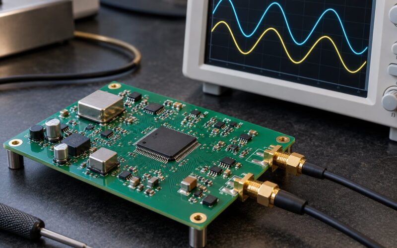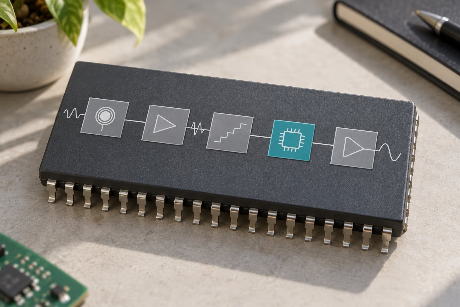
Analog and mixed signal IP explained in one line: it is licensable, pre-verified circuit design for the parts of a chip that live in the continuous world, plus the digital control logic that manages them. Analog IP covers amplifiers, filters, references and data converters. Mixed-signal IP wraps those blocks with registers, calibration and bus interfaces so a digital team can drive them.
Below is the mental model I wish more procurement conversations started with. What the IP actually is, how it is delivered, what it costs you in integration effort, and where it quietly breaks.
Table of Contents
- What Is Analog and Mixed Signal IP?
- How Analog and Mixed Signal IP Differs from Digital IP
- What Blocks Make Up Typical Analog and Mixed Signal IP?
- How Analog and Mixed Signal IP Is Designed
- Which Specifications Matter Most for IP Quality?
- Analog and Mixed Signal IP Explained Through a Sensor Interface Example
- How Is Analog and Mixed Signal IP Integrated into an SoC?
- How Do PDKs, Foundries, and IP Vendors Work Together?
- How Is Analog and Mixed Signal IP Verified?
- When Should a Team Use IP Instead of Designing Its Own?
- Frequently Asked Questions
- Is analog and mixed-signal IP delivered as RTL?
- How is mixed-signal IP different from digital RTL IP?
- What does it mean for analog IP to be foundry-qualified?
- Can analog and mixed-signal IP be used across process nodes?
- How much customization is usually included with licensed IP?
- Conclusion
What Is Analog and Mixed Signal IP?
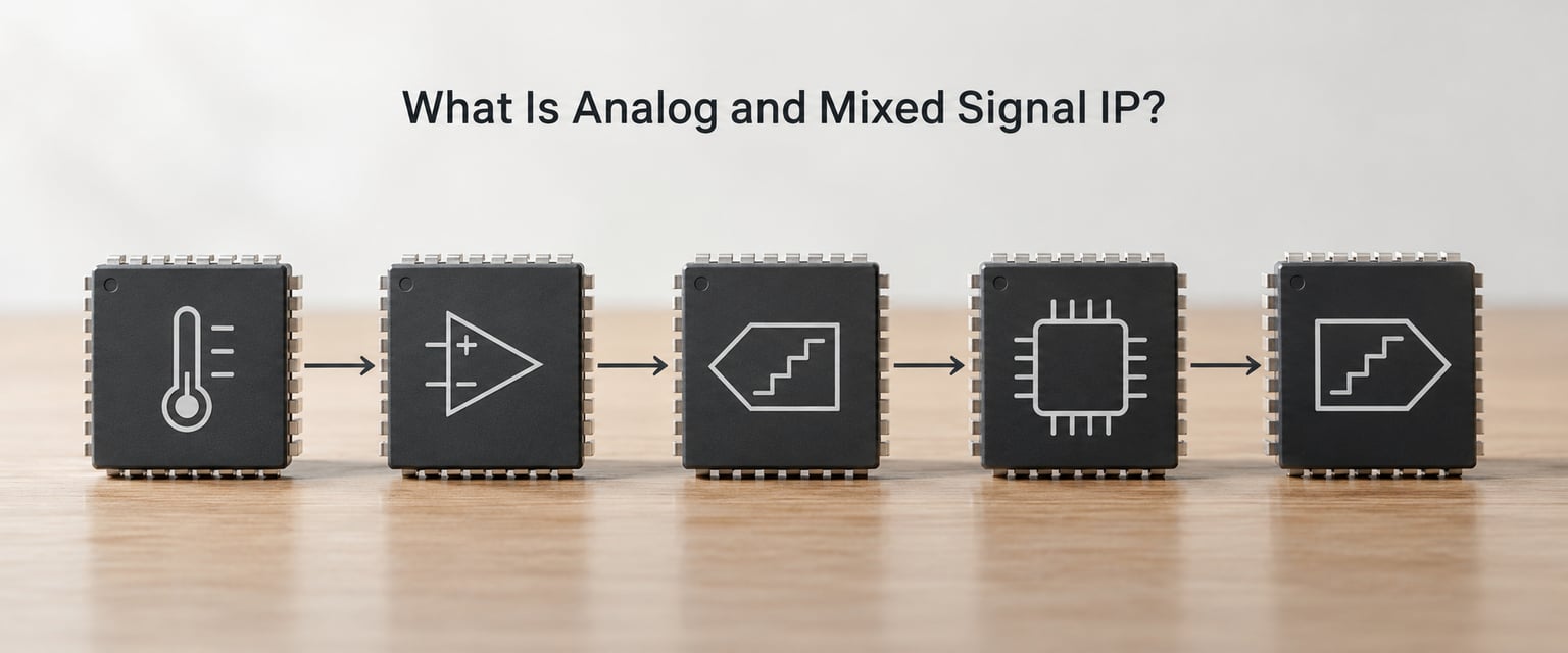
Analog and mixed signal IP is a reusable block of circuit design that a vendor has already built, characterized and verified, and that you license into your own chip. Analog IP handles continuous quantities such as voltage, current and time. Mixed-signal IP adds digital control around that analog core, so the block arrives with configuration registers, calibration logic and a standard bus.
The word IP here means intellectual property, not internet protocol. It is the same term used for digital RTL cores, processor architectures and SerDes. What changes with analog is the delivery: a digital core is mostly portable source code, while an analog block is tied to the device models and layout rules of a specific process.
Consider a temperature sensor reading on a wearable. The die holds a bias circuit, an amplifier, a low-pass filter, a sigma-delta or SAR ADC, a digital calibration routine and a control block that reports over I2C. Nobody licenses the whole thing. Teams mix and match: buy the ADC and the reference, build the bias network in-house because it depends on their sensor process.
Why license at all? Because analog design resists automation, needs engineers who are scarce and expensive, and rarely gets cheaper when the node shrinks. Every node change can move gain, offset and noise. Licensing proven IP compresses schedule and cuts the risk of a failed tape-out in the part of the design that is hardest to debug on real silicon.
How Analog and Mixed Signal IP Differs from Digital IP
The difference is not cosmetic. Digital logic is described as boolean functions and mapped to standard cells automatically. Analog behavior depends on device physics, matching, temperature and layout, which is why the design flows, the verification methods and the reuse models all diverge.
| Dimension | Analog | Digital | Mixed-signal |
|---|---|---|---|
| Signal type | Continuous in time and amplitude | Discrete samples at defined logic levels | Both, crossing at converters and interfaces |
| Primary design inputs | Device models, matching, thermal limits | Timing, area, power targets | Both sets, plus the interface between them |
| Verification | SPICE and AMS corner simulation, measurement | Logic simulation, formal, timing sign-off | Co-simulation plus analog metrics plus digital checks |
| Layout sensitivity | High: routing and grounding change the result | Low: cells are characterized and interchangeable | High in the analog domain, negligible in the digital |
| Benefit from node scaling | Limited, and often reversed by lower supply voltage | Strong: density and power improve each node | Digital half scales, analog half mostly does not |
| Reuse across foundries | Requires porting and re-qualification | Often source-portable | Porting cost dominated by the analog blocks |
| IP availability | Specialist vendors and in-house teams | Large mature vendor ecosystem | Mixed; usually the least commoditized |
Two misconceptions are worth clearing up. First, analog and digital are never fully independent on a die: they share a substrate, share supply rails, and inject noise into each other. Second, a “mixed-signal” block is not a new physics. It is an analog core plus enough digital logic that a processor can configure, calibrate and read it.
That coupling shows up in the noise floor. Digital switching current flowing through the substrate can appear as an analog input perturbation large enough to swamp a microvolt-level signal. Practitioners on mixed-signal design forums describe this as one of the most stubborn practical problems, and it is why fully differential topology, guard rings, triple-well isolation and on-chip decoupling are standard practice rather than options.
What Blocks Make Up Typical Analog and Mixed Signal IP?
Most licensable blocks fall into a small number of families, and each family has a characteristic set of metrics. Knowing the family tells you what to specify, what a vendor’s datasheet should contain, and whether the block can be reused across projects.
| Block | Main job | Typical metrics | Common delivery model |
|---|---|---|---|
| Operational amplifier | Amplify a small differential signal | Gain, GBW, noise density, offset, input capacitance | Hard IP or parameterized generator |
| Filter | Shape the frequency content of a signal | Corner frequency, stopband attenuation, passband ripple | Generator-based, switched-capacitor or continuous-time |
| SAR ADC | Sample and convert, medium to high rate | Resolution in bits, sample rate in MSPS, SNR, ENOB, input range | Hard IP with digital wrapper |
| Sigma-delta ADC | High resolution from a narrow bandwidth | Bits, oversampling ratio, output data rate, clock range | Hard IP with digital decimation filter |
| DAC | Generate an analog output from digital code | Resolution, settling time, INL/DNL, output range, reference accuracy | Hard IP with digital wrapper |
| Voltage reference | Produce a stable, temperature-independent voltage | Initial accuracy, drift in ppm per degree C, PSRR, start-up time | Hard IP, usually the hardest block to replace |
| Oscillator and PLL | Create and multiply clocks, deliver clean references | Frequency range, phase noise, jitter, lock time, reference spur | Hard IP, heavily PDK-qualified |
| Clock and data recovery | Recover timing and data from a serial link | Data rate, jitter tolerance, lane count, recovery latency | Hard IP or SerDes PHY |
| Interface controller PHY | Talk to off-chip devices and boards | Bus type, speed, IO standard, ESD rating | Hard IP or soft IP with pad collateral |
| Power management unit | Convert, regulate, sequence and monitor supplies | Efficiency, quiescent current, output accuracy, load transient, drop-out | Soft IP or generator-based subsystem |
| PVT sensor | Report supply voltage, process and temperature on die | Accuracy range, resolution, readout interface, calibration | Hard IP with calibration logic |
| Sensor interface | Bias, excite and read a physical sensor | Input range, offset and drift, excitation noise, gain | Design service more often than catalog IP |
A useful observation from teams that license heavily: converters and interfaces are the most commoditized, while the bias and reference blocks around them are the most custom. The reason is that the reference sets the accuracy ceiling for the entire chain. A 14-bit converter behind a drifting reference is not a 14-bit converter at temperature extremes.
How Analog and Mixed Signal IP Is Designed
Analog and mixed signal IP is designed by iterating against simulation until the numbers hold across every corner, then proving it again after layout. There is no clean path where a specification becomes netlist automatically. Each stage feeds back into the one before it.
Requirements come first, and they are written as measured quantities rather than adjectives. “12-bit ADC” is not a specification; “12-bit ADC, 2 MSPS, 70 dB SNR at the input, 200 kHz analog bandwidth, works from 1.8 V to 3.6 V, -40 C to 125 C” is.
Architecture next. A designer picks topology: switched-capacitor versus continuous-time filtering, charge-redistribution SAR versus pipeline versus sigma-delta conversion, single-ended versus fully differential. This decision constrains everything downstream, including the clock, the reference and the layout style.
Sizing and schematic design follow, device by device. Transistor widths, current branch ratios, resistor and capacitor values, and matching intent get set here. Then device-level simulation: transient, AC, noise, DC sweep, Monte Carlo mismatch, and behavior across the foundry’s characterization corners.
Layout is where the design gets honest. Guard rings, isolation wells, differential symmetry, on-chip decoupling, matching of sensitive pairs and clean grounding decide whether the extracted circuit matches the schematic one. Back-annotation with extracted parasitics and a repeat of the corner simulations is where most surprises appear.
Why does this differ so much from a digital flow? Because synthesis has a well-defined mapping from RTL to a characterized cell library with bounded delay and power. An analog block has no equivalent automatic mapping. Its performance lives in device parameters, matching statistics and physical placement, so iteration is manual, and each layout change can reset the electrical result.
Which Specifications Matter Most for IP Quality?
Quality is visible in a small set of numbers per block type. Ask for these before asking for features, because the features are usually present and the numbers are usually optimistic.
| Specification | Applies to | Why it matters |
|---|---|---|
| Supply voltage range | All blocks | Sets the achievable swing and linearity at the extremes |
| Current consumption | All blocks | Drives battery life and thermal design in the SoC |
| Effective number of bits | Converters | Real performance after noise and nonlinearity, not the label on the box |
| SNR and THD in dB | Converters, amplifiers | The number that actually limits signal fidelity |
| Input-referred noise density | Amplifiers, references | Sets the noise floor of the whole analog front end |
| Offset and drift | Amplifiers, references, sensors | Drift determines accuracy over temperature, not just at 25 C |
| Bandwidth and settling time | All blocks | Must match the system clock and signal bandwidth |
| Start-up time | References, regulators, PLLs | Determines how fast the system is usable after power-on |
| Layout-dependent sensitivity | High-gain and high-impedance nodes | Shows whether the design was signed off post-layout or only on the schematic |
| Interface format | Digitally wrapped blocks | A block on a proprietary bus costs you integration weeks |
| Area in the target process | All blocks | Analog area rarely shrinks; it competes with digital logic for die budget |
| Verification coverage | All blocks | Evidence of corner, mismatch and post-layout sign-off, not just functional tests |
Analog and Mixed Signal IP Explained Through a Sensor Interface Example
Take a temperature sensor in a battery-powered wearable and walk the numbers through. A sensor with a sensitivity of roughly 1.8 mV per degree C sits behind a bias circuit that sets its operating current. The choice of bias current trades signal amplitude against self-heating and power draw, and on a coin-cell design that trade is made every day.
Next, the amplifier. A fully differential topology with a gain of around 100 lifts the sensor’s few hundred millivolts into a range the converter accepts, and its offset and drift set the floor on achievable accuracy across temperature. Offset is often removed later by calibration, but drift cannot be calibrated away in the same way, which is why the amplifier’s thermal behaviour matters more than its room-temperature offset.
The filter then decides what the converter has to deal with. A low-pass filter ahead of the ADC removes switching noise injected from the digital side of the die. Without it, switching spurs land inside the signal band and quantization error stops being the limiting noise source.
The ADC resolves the filtered voltage. Resolution in bits sets the ideal quantization noise floor; SNR and ENOB tell you how close the real converter gets to that floor at a given sample rate. If the band is narrow and the required resolution is high, a sigma-delta modulator with digital decimation is the usual answer, because it trades sample rate for resolution cheaply.
The reference voltage sets the top of the converter’s input range, so its initial accuracy and temperature drift bound the accuracy of the entire measurement. A high-resolution converter with a sloppy reference is wasted silicon.
Digital calibration then removes constant offset and gain error using stored coefficients, loads a PID loop or lookup table, averages samples to suppress noise, and pushes the final value over I2C. That is the mixed-signal handover point: the analog chain defines what is knowable, and the digital side decides how much of it is actually extracted.
Verification overlaps at exactly that boundary. Digital engineers verify the register map and the calibration algorithm. Analog engineers verify gain, noise and drift. The mixed-signal checks confirm that the algorithm compensates what the circuit actually produces, measured across corners and at the intended clock rates.
How Is Analog and Mixed Signal IP Integrated into an SoC?
Integration starts with the interface contract, not the schematic. A licensed block arrives with expected register behavior, clock frequency limits, reset requirements, supply sequencing rules, and a list of pins it needs from the rest of the chip. Teams that skip this document discover the mismatches late, in layout, when changes are expensive.
Supplies and grounding need deliberate planning. Analog and digital rails may run at different voltages with different noise requirements, so each block needs a clear filter, local decoupling and a defined return path. Sharing one rail without filtering is a common source of the substrate coupling problems described earlier.
Clocking and reset have their own rules. Mixed-signal blocks often need a stable reference with bounded jitter, and they may need specific power-on timing to release internal bias circuits correctly. Reset strategy, whether asynchronous, synchronous or a mix, must match the vendor’s expectation or the block’s calibration state can be invalid at startup.
Placement is a performance decision, not a packing decision. Analog blocks need their own power island, guard rings and space for guard traces, and they need to sit away from the noisiest digital blocks. Sensitive routing such as reference and clock distribution is matched and shielded, because a few milliohms of trace resistance changes the reference more than most datasheet notes admit.
Package effects get considered too. Substrate, bond wires or flip-chip bumps add capacitance and coupling that were not in the on-die simulation, and they change with the package choice. At top level, the whole thing goes through mixed-signal sign-off: extraction, IR drop and electromigration analysis, post-layout corner simulation, and a system-level check that clocking, resets and supplies come up in the required order.
How Do PDKs, Foundries, and IP Vendors Work Together?
A process design kit is the contract between a foundry and a design. It contains device models, layout rules, extracted views, standard cells, characterized memories, and the statistical corners the process is expected to meet. Foundries also compile memories and supply their own interface IP, because those blocks need intimate knowledge of the process.
IP vendors take the PDK, build and verify a block against it, then deliver a package the customer can drop into their flow: views for schematic capture and simulation, layout collateral, timing and parasitic models, documentation and a set of characterized test results. EDA suppliers sit alongside this, providing the simulators, layout tools and verification environments the whole thing depends on.
What varies most between vendors is portability. Some blocks are described as process-agnostic, built from a generator that recomputes sizing and layout for a target PDK from a seed design. Others are qualified for one process on one foundry, and are the highest-performance option precisely because the whole thing was tuned to that device set.
Be clear about which one you are buying. Process-agnostic IP trades some peak performance for the ability to retarget when a process is unavailable or when the product needs to move. A foundry-qualified block gives the better result on that process and raises your cost if you ever port. Ask for the qualification evidence: which corners were simulated, whether post-layout sign-off was done, and on which revision of the PDK.
Vendor offerings change. Confirm the current process list and supported flows directly with the supplier rather than relying on a marketing page or a document from a previous project.
How Is Analog and Mixed Signal IP Verified?
Analog verification is measurement, not pass and fail. Each block is characterized against a specification at every corner the product must survive, and the results are reported rather than inferred.
At block level, engineers run transient, AC, DC, noise and transient-noise simulations across the process, voltage and temperature corners defined in the foundry’s PDK. Monte Carlo analysis covers random mismatch. Functional coverage then checks every mode, calibration state and error path in the register map.
Mixed-signal verification adds co-simulation. The analog core is modeled in a language such as Verilog-AMS or VHDL-AMS, connected to the digital testbench, and simulated together so the system-level behavior is checked with real analog behavior rather than an idealized model. This is where interface errors surface: reset timing, handshake deadlocks, calibration data that never converges.
Sign-off then repeats the critical measurements with extracted parasitics after layout, adds IR drop and electromigration analysis, and checks that the block meets specification with layout-dependent effects included. The gap between schematic-only results and post-layout results is exactly where surprises live, and a vendor that will only show you the first one has not finished the job.
On silicon, the story continues. Built-in self-test and on-chip calibration let the device measure itself at production test, which is how analog performance over product lifetime is tracked: trim values are stored in fuses or registers at test and read back in the field for diagnostics. Test benches for mixed-signal parts cost real money, and building them is often a bigger effort than the block itself.
When Should a Team Use IP Instead of Designing Its Own?
Use IP when the block is not where your differentiation lives, and design it when it is. The rest of this section is the version of that sentence with the trade-offs written out, because the honest answer is a spreadsheet rather than a rule.
| Approach | Wins when | Watch out for |
|---|---|---|
| Buy hard IP | Schedule matters most and the process is fixed | Least flexibility; block is a black box you cannot resize |
| License soft IP | You need to modify, size or wrap the block yourself | Integration and verification effort moves onto your team |
| Use a generator or parameterized IP | Specifications vary per product and the process may change | Generation and sign-off effort on each new configuration |
| Design in-house | The block defines product advantage, or volumes are low and customization total | You need analog engineers you probably cannot hire quickly |
| Design service engagement | You need the block built and characterized but have no in-house team | Longer schedule; you own the project management |
| Mixed-signal FPGA or PSoC prototype | Volumes are low or the design is still uncertain | Per-unit cost stays high; power and size are worse than an ASIC |
The economics behind this: a license fee buys you a headcount you would otherwise have to hire, plus a schedule you would otherwise lose. Licensing models follow the same split. Some charge an upfront fee only, some charge a royalty per shipped unit, and customization is usually a separate one-time effort plus support. Contracts vary, so treat any specific figure you hear as anecdotal and check the current terms yourself.
The real cost nobody puts in the spreadsheet is integration. Adding a vendor block means you inherit their interface, their corner assumptions, their verification gaps and their support model. Ask what happens when the block fails a corner your product needs, who owns the fix, and whether you get the behavioral model and the testbench as part of the delivery.
The strongest reason to design in-house is that analog rarely improves with reuse across products the way digital logic does. If the block is your differentiator and your process is unusual, in-house work pays back. If it is a commodity block on a standard process, you are spending scarce analog talent on something a vendor has already tuned across dozens of designs.
Frequently Asked Questions
Is analog and mixed-signal IP delivered as RTL?
Usually not in the digital sense. A typical mixed-signal block ships as a schematic-level design, layout views, extracted models and simulation models for the target process, plus a digital wrapper for configuration and readout. Some vendors deliver Verilog-AMS or VHDL-AMS models so the block can join a mixed-signal testbench, and some offer source-level soft IP that you can modify. Only the digital control logic inside the block is RTL.
How is mixed-signal IP different from digital RTL IP?
Digital RTL IP is portable source that synthesis maps onto any characterized cell library, so reuse is close to free across foundries. Analog and mixed-signal IP is tied to a process: its performance depends on device models, matching statistics and layout. Porting it means re-sizing, re-laying out and re-verifying against a new set of corners, which is why qualification is a real cost rather than paperwork.
What does it mean for analog IP to be foundry-qualified?
It means the vendor has run the block on a specific foundry process and PDK revision and can show measured results across the process, voltage and temperature corners, including post-layout parasitic extraction. Ask which corners were covered, whether layout-dependent effects were included, and whether the results were measured on silicon or only simulated. Qualified blocks perform better on that process and cost more to move elsewhere.
Can analog and mixed-signal IP be used across process nodes?
Only with work. Porting to a different process or node means resizing devices, reselecting device types, adjusting supplies and clocking, re-laying out for the new rules, and repeating corner simulation and sign-off. Generator-based and process-agnostic products automate much of that step, which is why they exist. Budget engineering time and re-verification for every port, and confirm that the vendor supports the target process before you design it in.
How much customization is usually included with licensed IP?
Assume none beyond configuration options exposed through registers: channel count, sampling rate, filter bandwidth, reference selection and clock dividers. Genuine structural changes, such as a different input range, extra channels, a new bus interface or a different supply domain, are normally handled as a separate customization engagement with its own schedule and fee. Ask the vendor to list what is configurable as delivered, and what requires a project, before you commit to a schedule.
Conclusion
The mental model to keep is simple. Analog and mixed signal IP is design you license instead of building: continuous-time circuits, plus the digital control that makes them usable, plus the evidence that they work at every corner. It is worth buying when the block is a commodity and your scarce people are digital specialists. It is worth building when the block is the product.
Start with the signal chain: write down the input range, the bandwidth, the required resolution and accuracy, and the output interface. Then fix the process and the corners, and only then compare vendors on delivery model and qualification evidence. Everything else in the decision, cost included, follows from those two steps.