Short answer: a CMOS image sensor beats a CCD in nearly every high-volume application because it reads each pixel out in parallel, uses far less power, and scales to higher frame rates. A CCD still wins in a few narrow roles — deep ultraviolet and near-infrared imaging, time delay and integration arrays, electron multiplication at very low signal levels — so this cmos image sensor vs ccd comparison is not a one-sided verdict.
Both technologies convert photons into electrical charge by the photoelectric effect. The difference lives in what happens next: how that charge is moved off the chip, converted to a voltage, and digitised. That single architectural choice ripples outward into noise, power, speed, shutter behaviour, how much circuitry you can bolt on afterwards, and what the sensor costs to build.
I have watched this argument go badly for twenty years, mostly because forum threads compare a 2005-era 5-megapixel CCD against a current 45-megapixel CMOS sensor and call the result a verdict. Below is the architecture-level comparison, followed by the applications where the answer genuinely changes.
Table of Contents
- CMOS Image Sensor vs CCD Comparison at a Glance
- How Do CMOS Image Sensors and CCDs Work?
- Charge readout is the whole argument
- The CMOS Image Sensor vs CCD Comparison in Six Differences
- Image Quality and Low-Light Performance
- What the “CCD look” actually is
- Power Consumption and Heat
- Readout Speed, Video, and Rolling Shutter
- Noise, Sensitivity, and Dynamic Range
- Size, Integration, and System Design
- Cost, Availability, and Longevity
- Which Should You Choose?
- Frequently Asked Questions
- Is CMOS always better than CCD for image quality?
- Which sensor uses less power, CMOS or CCD?
- Are CCD cameras still worth using today?
- What is the main difference in rolling shutter and video performance?
- How do I choose between CMOS and CCD for a camera or machine-vision system?
- Conclusion: Start With the Application
CMOS Image Sensor vs CCD Comparison at a Glance
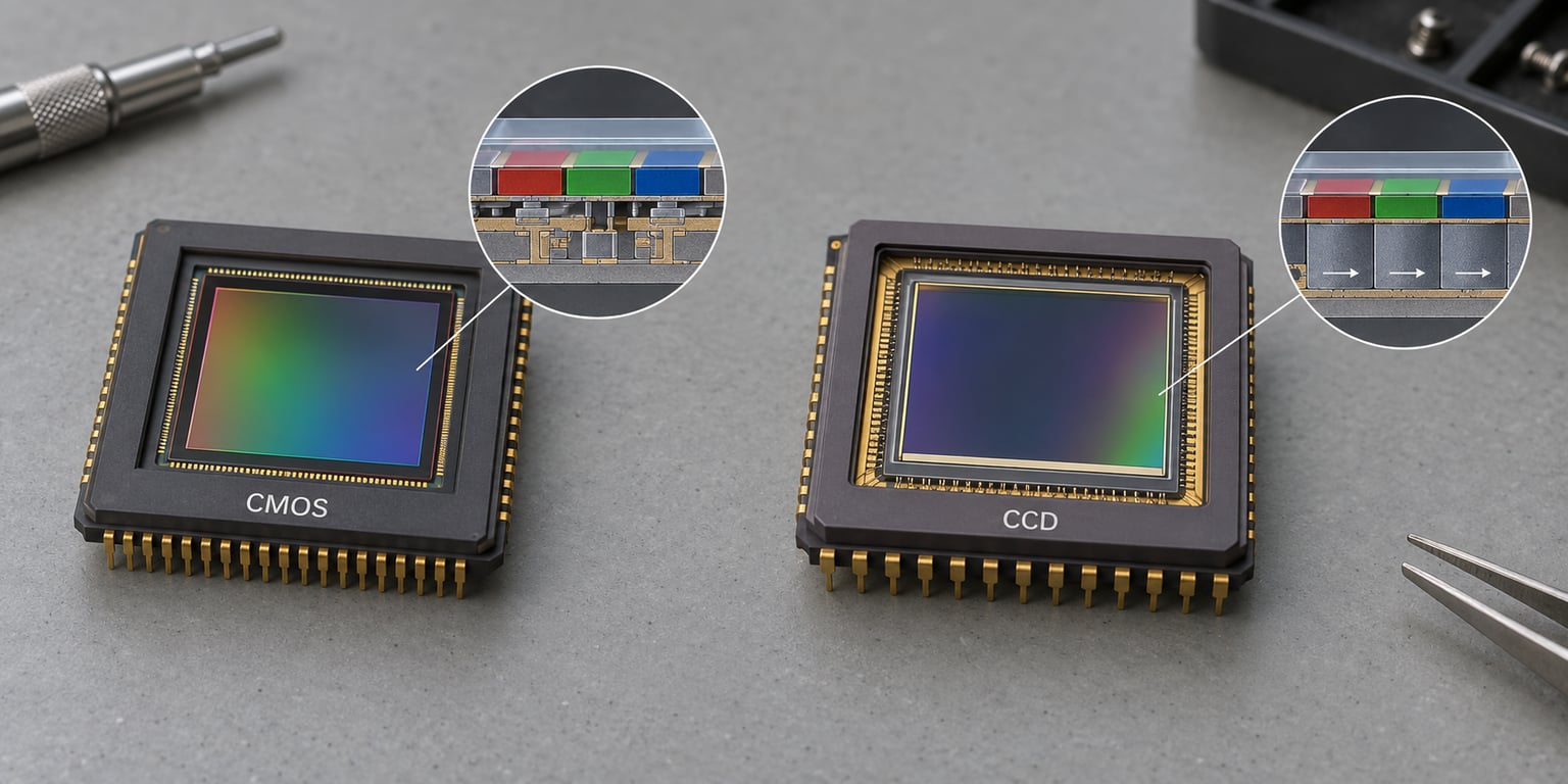
If you only read one thing, read the table. CMOS wins power, speed, integration and cost at volume; CCD wins in a small set of spectral and very-low-light niches where its architecture is still the easier engineering choice.
| Attribute | CCD | CMOS |
|---|---|---|
| Charge readout | Serial, shifted register by register to one output node | Parallel, each pixel converted and read on its own column |
| Pixel type | Passive pixel, photodiode only | Active pixel, photodiode plus amplifier and reset |
| Output signal | Analog at the output amplifier | Digital, column-level ADC on the same chip |
| Power consumption | High, the whole array clocks continuously during transfer | Low, typically a fraction of CCD draw, often up to two orders of magnitude less |
| Read noise | Very low, one or a few amplifiers serve the whole array | Low, more amplifiers but each runs at lower bandwidth |
| Frame rate ceiling | Limited by serial transfer time | High, set by parallel column bandwidth and interface |
| Shutter | Global shutter standard | Both global and rolling shutter available |
| On-chip processing | Minimal | Column ADC, black correction, HDR, sometimes full ISP |
| Blooming and smearing | Possible at saturation | Largely eliminated by pixel-level charge-to-voltage |
| Unit cost at volume | Rising as fabs exit the process | Low, made on mature high-volume logic lines |
| Custom design NRE | Lower, fewer masks, simpler process | Higher, deep submicron logic mask set costs more |
| Best fit | NIR, deep UV, TDI, EMCCD, some scientific instruments | Phones, DSLRs, machine vision, robotics, medical, security, video |
One caveat on the power row. Vendors quote figures like “up to 100x less” for CMOS, and that range is real for the sensor element itself under continuous readout, but a finished camera also spends power on image processing, memory and radios. Treat the ratio as an architecture signal, not as a battery-life promise for a finished product.
How Do CMOS Image Sensors and CCDs Work?
Both start the same way. A photon hits a photodiode built in silicon, knocks an electron loose, and the electron falls into a potential well where it waits until readout. The difference is everything that happens after the well fills.
Charge readout is the whole argument
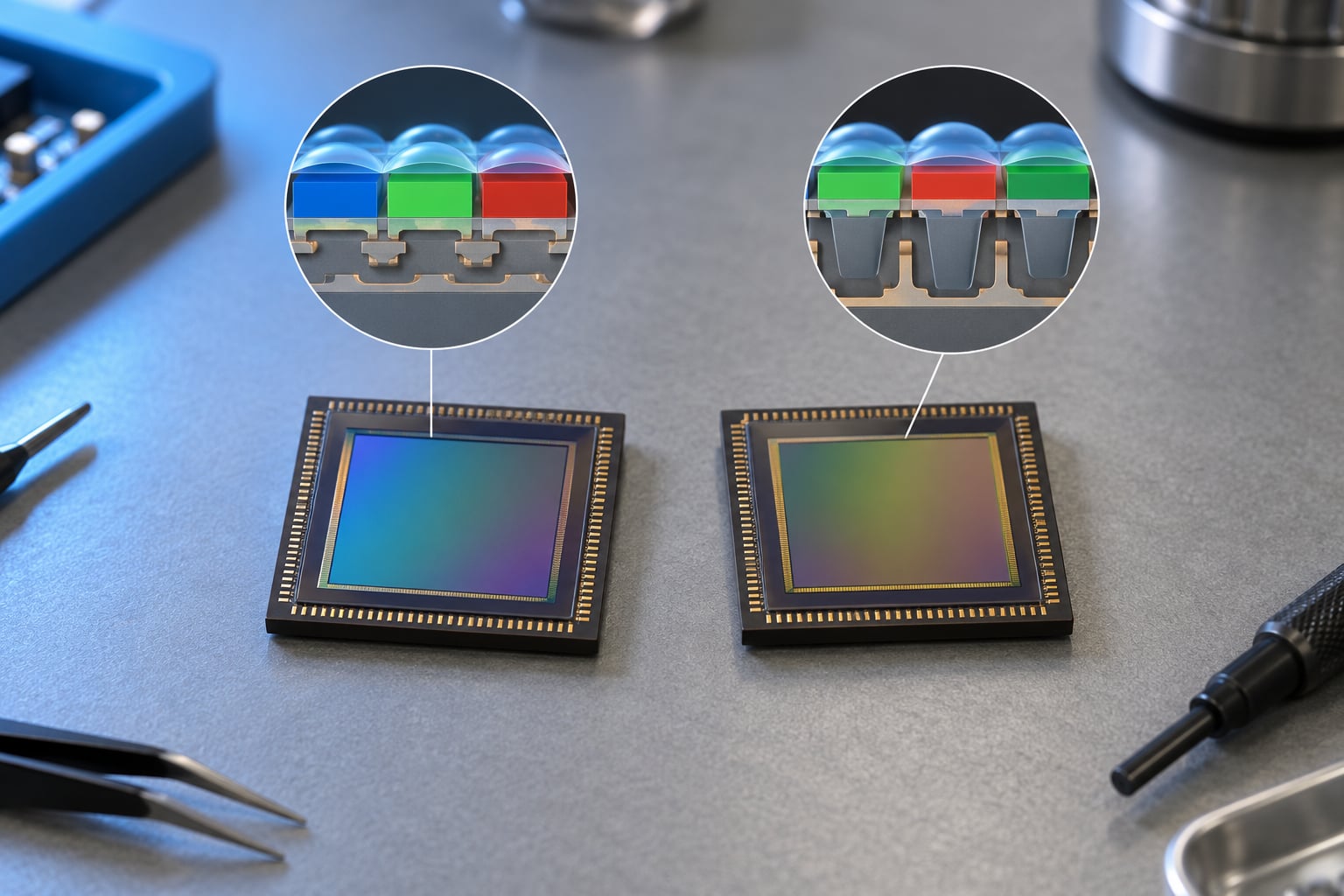
In a charge coupled device, the pixel itself is mostly empty space. It holds a photodiode and little else. When exposure ends, a clocked voltage sequence shifts each packet of charge sideways into the neighbouring register, and it keeps going — row after row, column after column — until everything arrives at a single output amplifier at the corner of the chip.
That serial shuffle is elegant and it produces excellent noise figures, because a handful of low-noise amplifiers serve the entire array. It also means the array is a clocked machine running during readout, and only one or a few output nodes exist, so total readout bandwidth is capped by how fast you can clock the shift registers.
In a CMOS image sensor, each pixel carries its own photodiode, reset transistor and amplifier. Charge becomes voltage right where it was collected, and a column-level analog-to-digital converter converts it to a number before it leaves the chip. Every column is read simultaneously, so the outputs are digital by the time they reach the pad ring.
This is why CMOS scales. Wafer fabs already make billions of transistors per wafer for processors, and a CMOS image sensor is designed on many of the same lines with the same design rules and EDA flows. A CCD needs its own specialised process.
The CMOS Image Sensor vs CCD Comparison in Six Differences
- Readout path: CCD shifts charge serially to one output node; CMOS reads each pixel directly on its own column.
- Pixel structure: CCD pixels are passive, containing a photodiode; CMOS pixels are active, adding an amplifier and reset transistor.
- Signal type at the output: CCD produces an analog voltage needing external digitisation; CMOS produces digital data from column ADCs on the die.
- Power and clocking: CCD clocks the whole array during transfer; CMOS only biases the columns being read, so draw scales with activity.
- Integration options: CCD is easier to build in time delay and integration and deep-UV architectures; CMOS is easier to build in stacked, backside-illuminated and on-chip-processing architectures.
- Manufacturing: CCD needs a dedicated process with few, large masks; CMOS runs on mature deep submicron logic lines with many small masks and cheap per-unit economics at volume.
None of this is new. Both devices date to the late 1960s and early 1970s. CCD won the first decades because it delivered cleaner images with the fabrication technology available at the time, and CMOS only caught up once active-pixel designs and column ADCs matured enough in the 1990s, driven largely by mobile phone investment.
Image Quality and Low-Light Performance
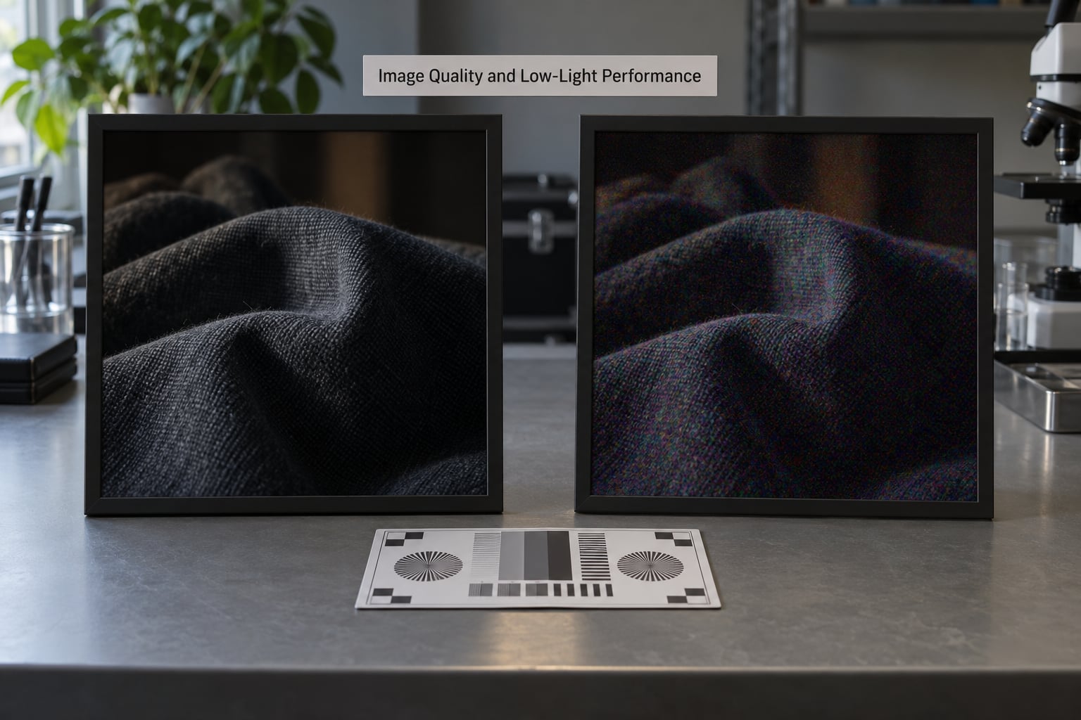
The honest answer here is that modern CMOS matches or beats CCD in almost every mainstream parameter, and the gap widened with each sensor generation. Both are monochrome devices underneath a colour filter array, so raw photon capture is comparable when pixel pitch, quantum efficiency and fill factor match.
Read noise is where the architecture shows. A CCD uses one or two amplifiers for the whole array, so those amplifiers can be slow, high-gain and very quiet. A CMOS sensor has thousands of amplifiers, one per column, which sounds worse until you notice each one only has to handle a few hundred pixels in a short window. Teledyne’s imaging team puts it neatly: amplifier noise scales inversely with bandwidth, so a massively parallel array running narrow-bandwidth amplifiers ends up quieter than a serial design running one wide-bandwidth amplifier. Modern column-parallel CMOS reaches single-digit electron read noise at room temperature.
Quantum efficiency has converged too. Backside-illuminated thinning and on-lens colour filters got most of the way there, and stacked CMOS sensors put the logic layer behind a thin pixel layer so fill factor no longer steals light.
What the “CCD look” actually is
The claim that CCDs render colour with more character is the most persistent myth in this field. Both sensor types are monochrome; colour comes from the colour filter array, the demosaicing algorithm, the tone curve and whatever processing sits downstream. Forum consensus has moved this way over the past several years, with long-running threads on photography forums and astronomy communities concluding that “CCD is better than CMOS” is simply incorrect for modern imagers.
What enthusiasts describe as the CCD look is usually down to a camera generation rather than a sensor architecture. It is an in-camera JPEG pipeline from the late 2000s, a specific demosaic implementation, and aggressive edge sharpening. Shoot both sensors in RAW with the same glass and the difference largely disappears.
Astrophotographers report the same thing in reverse: people who moved from CCD to CMOS astro cameras usually point to short sub-exposure lengths as the cause of extra noise, not the sensor itself.
Power Consumption and Heat
This is CMOS’s cleanest win, and it is an architectural win rather than a manufacturing one. A CCD runs a multi-phase clock across the entire array for the duration of every readout, which takes real power whether or not useful data is coming out. A CMOS sensor powers only the columns being read, and a still frame can leave most of the die idle.
Two secondary effects matter in embedded work. First, CMOS sensors use a low core voltage, usually around 1 to 1.8 V, which simplifies power supply design and cuts heat in sealed housings. Second, because the sensor produces digital data, the same supply rail can power the column ADCs without a separate analog island or external digitiser with its own clock domain.
That directly affects battery life in drones and handheld inspection tools, and it removes the need for a heatsink in sealed camera bodies. In a space or medical instrument, lower dissipation also means less thermal mass near the sensor, which keeps dark current predictable.
Readout Speed, Video, and Rolling Shutter
A CCD moves every pixel through a serial pipeline, so its maximum frame rate and full-resolution bandwidth are limited by register clocking. A CMOS sensor reads all columns in parallel, so the ceiling comes from amplifier bandwidth, the column ADC, and the output interface — typically MIPI, LVDS or parallel CMOS in industrial parts.
That parallelism is what made high-frame-rate video, global-shutter machine vision and stacked mobile sensors possible. It is also why CMOS won the video camera market outright.
| Shutter behaviour | How it happens | What it does to your footage or measurement |
|---|---|---|
| Global shutter (CCD) | Whole array accumulates and empties together | No skew in fast motion; the long-standing CCD advantage for cinematography and inspection |
| Global shutter (CMOS) | On-chip control gates stop the whole array at once | Same geometry as CCD, now with CMOS power and speed; common in industrial sensors |
| Rolling shutter (CMOS) | Rows read out top to bottom over the frame interval | Warp on fast pans and machine-vision motion; sometimes mitigated with a scan or readout-mode switch |
Cinematographers on professional forums still name rolling shutter as CCD’s lasting practical advantage, and it is a real one for handheld work. The catch is that the advantage now belongs to CMOS variants that offer a global shutter, not to the CCD architecture itself.
Noise, Sensitivity, and Dynamic Range
Four different things get called noise, and separating them makes the comparison much cleaner.
Shot noise is physics. It scales with the square root of the signal, so it affects both technologies equally and is the floor you cannot engineer away. Read noise is added by the readout electronics, and as covered above, modern column-parallel CMOS has closed the gap with CCD. Dark noise comes from thermally generated electrons and depends on temperature, sensor architecture and how long the array integrates.
Full well capacity — how many electrons a pixel can hold before saturating — depends on pixel size and pixel pitch rather than on whether the sensor is CCD or CMOS. Dynamic range follows from full well against the noise floor, so it too is not automatically a CCD advantage. Binning and long exposure recover it in the CCD case; column-parallel readout and in-sensor averaging recover it in CMOS.
The practical lesson is that nominal pixel size alone tells you very little. Two sensors with identical diagonals can behave completely differently depending on quantum efficiency at your wavelengths, the technology generation, and the cooling state. Specify on quantum efficiency and read noise at your working temperature, not on the marketing resolution.
Size, Integration, and System Design
CCD demands external help. You get an analog voltage from a small number of output nodes, so the system needs a separate analog-to-digital converter, a clock generator and usually a correlated-double-sampling front end. That is more board area, more power, and more parts to qualify.
CMOS brings the digital chain onto the die: column ADC, black-pixel and column-noise correction, binning and summation modes, and on larger parts an integrated image signal processor with tone mapping and HDR. A CMOS sensor is often closer to a finished imaging subsystem than a raw light detector.
The architectural direction of travel is stacked CMOS. A pixel wafer is bonded to a logic wafer, either face to face or back to back, so the amplifier and ADC sit under every photodiode. That removes the transistor from the optically active area, lifting fill factor, and it separates an aggressive logic process from a photo-optimised imaging process. Three-dimensional stacked and wafer-bonded CMOS is the reason monolithic CCD architecture stopped evolving. Basler and Teledyne’s learning centre materials make the same point without using the word.
Cost, Availability, and Longevity
Neither technology has a single price, and quoting one without resolution, performance tier and volume would be misleading. What differs is the shape of the cost curve.
For NRE, CCD is cheaper to customise. Fewer masks, a simpler process and a less demanding design mean a custom CCD can be brought up faster and for less than an equivalent custom CMOS image sensor, whose deep submicron logic mask set is expensive to prepare.
For unit cost at volume, the relationship reverses. CMOS image sensors run on mature logic lines with high devices-per-wafer counts and good yield learning, so per-unit cost drops steeply as volume rises. CCD manufacturing capacity has been winding down for over a decade, which pushes both unit prices and lead times up and removes the volume curve you were counting on.
For lifecycle planning, the asymmetry matters more than the numbers. A new CMOS design has a supplier ecosystem, a roadmap and, increasingly, second sources. A new CCD design risks being stranded on a part that no longer has a second source and no process after the current fab exits. Engineers specifying CCDs for ten-year industrial or aerospace programs should treat supply security as a design requirement, not a procurement detail.
One cost asymmetry runs the other way: a custom CMOS image sensor is expensive to start, but the on-chip integration it enables often deletes external board and components. Run the numbers on the whole system, not just the sensor line item.
Which Should You Choose?
Start with the application, not with the sensor architecture. In practice the decision looks like this.
| Application | Verdict | Why |
|---|---|---|
| Smartphones and wearables | CMOS | Stacked BSI design, tiny footprint, on-chip ISP |
| Digital cameras and video | CMOS | Frame rate, power, rolling and global shutter options |
| Machine vision and inspection | CMOS | Global shutter parts, high frame rates, small form factor |
| Robotics and warehouse automation | CMOS | Power budget and latency beat CCD efficiency gains |
| Medical imaging | CMOS | Compact, low-power, regulatory-friendly supply chain |
| Surveillance and security | CMOS | Infrared-friendly silicon, low power, long availability |
| Astrophotography | CMOS | Lower cost, no calibration frames, fast download |
| Space and remote sensing | CMOS, with exceptions | Radiation-tolerant CIS parts exist; CCDs remain in some instruments |
| Near-infrared imaging | CCD still common | Deep epi layers give strong NIR quantum efficiency |
| Deep-UV, TDI and EMCCD | CCD | Architecture is simpler for these specific jobs |
A short checklist to run before you commit. Frame rate and shutter type first, because they eliminate options fastest. Then low-light behaviour at your operating temperature, measured as quantum efficiency and read noise. Then the power budget including cooling. Then integration: what interface, how much external circuitry, what goes on the logic die. Then unit cost against expected volume, and finally supply security against your product’s expected life.
If your answer to the first question is “moderate frame rate, wide dynamic range, ordinary visible light, and we would rather not manage a bespoke readout”, take CMOS. If your answer involves wavelengths a thick silicon epi layer handles better, an integration scheme that only exists in CCD, or an existing qualified supply chain, keep CCD and document why.
Frequently Asked Questions
Is CMOS always better than CCD for image quality?
No. Modern CMOS sensors match or exceed CCDs in read noise, dynamic range and quantum efficiency for most visible-light work, so CMOS is usually the better answer. CCDs still hold advantages in near-infrared and deep-ultraviolet wavelengths, in time delay and integration arrays, and in electron multiplication at very low signal levels. Match the sensor to the wavelength, the integration scheme and the cooling budget rather than treating one architecture as universally superior.
Which sensor uses less power, CMOS or CCD?
CMOS uses substantially less power, often by a large multiple, because it clocks only the columns being read and produces digital data from on-chip column ADCs. A CCD must clock the entire array during serial transfer regardless of activity, and needs external conversion circuitry. Vendors quote figures as high as 100x less for the sensor element, though a finished camera’s total draw is dominated by processing, memory and connectivity.
Are CCD cameras still worth using today?
Yes, in specific niches. CCDs remain the practical choice for some near-infrared and deep-ultraviolet imagers, time delay and integration line scan arrays, electron multiplication cameras, and scientific or space instruments built on an existing qualified supply chain. For consumer cameras, machine vision, robotics, medical devices and security, CMOS has replaced CCD almost everywhere. New consumer-facing designs should default to CMOS.
What is the main difference in rolling shutter and video performance?
CCD sensors are almost always global shutter, so the whole array stops and restarts together and fast motion stays geometrically true. CMOS sensors come in both types, and rolling-shutter parts read rows top to bottom, which skews fast pans and moving objects in machine-vision measurements. Cinematographers often cite this as CCD’s last real advantage, but global-shutter CMOS sensors now offer the same behaviour with much lower power draw.
How do I choose between CMOS and CCD for a camera or machine-vision system?
Work through the requirements in order: frame rate and shutter type, then low-light behaviour measured as quantum efficiency and read noise at your operating temperature, then the power and cooling budget, then interface and how much external circuitry you can accept. Only after that look at cost against volume and supply security. If none of the CCD-specific advantages apply, CMOS is the lower-risk choice for a new design.
Conclusion: Start With the Application
Evaluate resolution, frame rate, shutter type, low-light performance, power budget, interface, cost at your volume, and supply life — in that order. In most cases the cmos image sensor vs ccd comparison ends quickly: begin with CMOS, and only specify a CCD where a specific strength or an existing compatibility case justifies it. Reviewed for 2026.