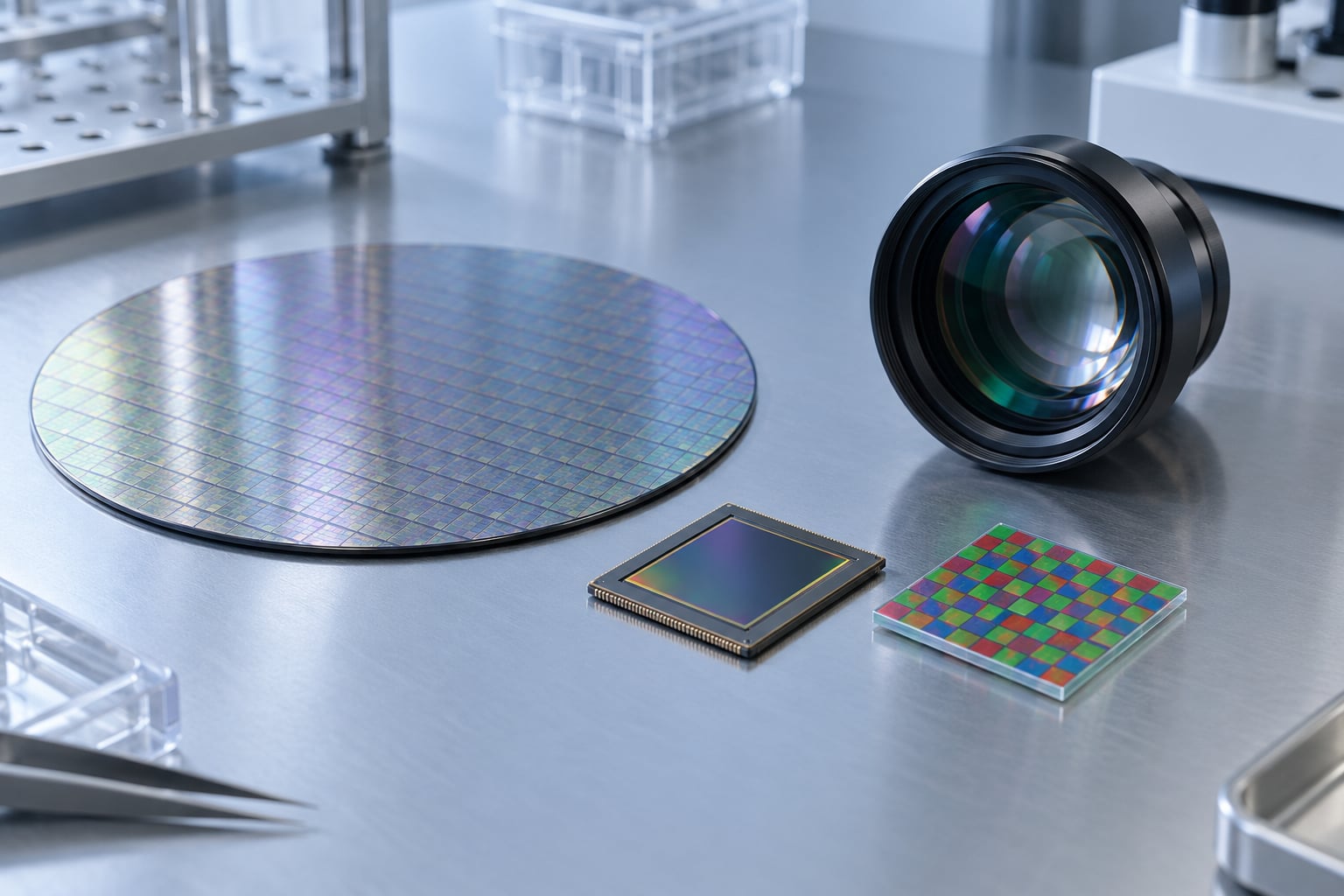
Image sensor manufacturing is the fabrication of a light-sensitive semiconductor chip on a silicon wafer: a grid of photodiodes and transistors built on a pixel wafer, bonded to a separate logic wafer, thinned from the back, then finished with an optical stack of color filters and microlenses. The die becomes an imaging component only after packaging, testing and lens attachment.
Most explanations stop at what a sensor does. This one follows how it gets built, step by step, because the manufacturing choices are the ones that decide sensitivity, power draw, dynamic range and cost. It is written for process engineers, sensor architects and the people who qualify camera modules for industrial, automotive and consumer products.
Table of Contents
- What Is Image Sensor Manufacturing?
- How Does an Image Sensor Convert Light Into Data?
- How Are CMOS Image Sensors Manufactured?
- What Are the Main Steps in the Manufacturing Process?
- Step 1: Wafer start and surface preparation
- Step 2: Front-end-of-line device formation
- Step 3: Interconnect and logic back end
- Step 4: Logic wafer fabrication
- Step 5: Wafer bonding
- Step 6: Wafer thinning and backside processing
- Step 7: Light-shield and aperture grid
- Step 8: Optical clear layers
- Step 9: Color filter array formation
- Step 10: Microlens formation
- Step 11: Dicing and package assembly
- Step 12: Wafer sort and final test
- How Are Color Filters and Micro-Lenses Made?
- What Does Binning Mean in Image Sensor Production?
- Why Do Sensor Size and Pixel Design Matter?
- How Does a Foundry Produce a Complete Camera Sensor?
- What Are the Main Manufacturing Challenges?
- How Do You Choose a Manufacturing Process for an Image Sensor?
- Frequently Asked Questions
- What process is used to manufacture image sensors?
- Are image sensors made using the same process as computer chips?
- What causes dead pixels in CMOS image sensors?
- How is a finished image sensor tested?
- Can a semiconductor foundry manufacture image sensors?
- Why do image sensors not always use the newest process node?
What Is Image Sensor Manufacturing?
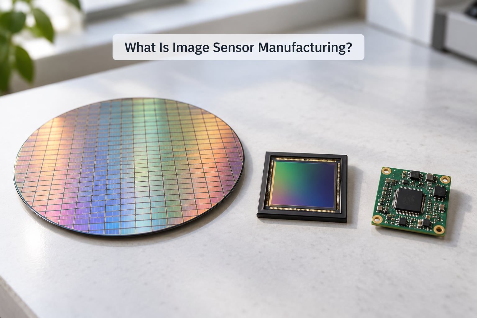
Image sensor manufacturing turns photons into a stream of numbers. A wafer fab builds the light-sensitive array, the readout electronics and the optical layers on top of them, then the die is cut, tested and mounted behind glass. The main product family today is the CMOS image sensor, which replaced the charge-coupled device in almost every new design.
Two other branches exist. Single-photon avalanche diode arrays, used for time-of-flight and depth sensing, run the photodiode above its breakdown voltage so a single carrier triggers an avalanche. Infrared sensors use different detector materials because silicon stops responding usefully past roughly 1.1 microns. Both still follow the same fab logic with a different front end.
What separates sensor production from logic-chip production is not the equipment list. It is the order of the modules, the thermal ceiling on the back end, and the size of the die. Sensors also need optical work that logic fabs do not do at all: a color filter array, a microlens array, an anti-reflective coating and alignment to a few hundred nanometres.
How Does an Image Sensor Convert Light Into Data?
A photosite is a photodiode paired with a few transistors. When a photon is absorbed in the depletion region, it frees an electron and leaves a hole behind. The pinned photodiode, the structure behind nearly every modern sensor, holds the hole away from the oxide interface so dark current stays low and the charge can be read without corrupting it.
A three-transistor pixel adds a reset, an amplifier and a select transistor. The reset transistor clears the node, the exposure runs for a set time, and the amplifier converts accumulated charge into a voltage. A fourth or fifth transistor is often added to hold reference charge or to split the charge, which is how most high dynamic range pixels work.
Columns of analog-to-digital converters sit beside the array, or in stacked designs inside the logic layer. They convert the analog voltage into a digital number, and the readout circuit walks the rows in sequence to send data out of the chip.
That sequential walk is why most sensors roll. Each row starts its exposure at a slightly different moment, so fast motion skews across the frame. Global shutter sensors park every row’s charge and release them together, which needs extra in-pixel or in-column circuitry, more silicon area per pixel and a stricter clock distribution across the die.
The raw output is a mosaic, not a picture. The color filter array gives each photosite one color, and a demosaicing algorithm in the image signal processor estimates the missing two channels from surrounding pixels. Everything between the photon and that reconstruction is decided during manufacturing.
How Are CMOS Image Sensors Manufactured?
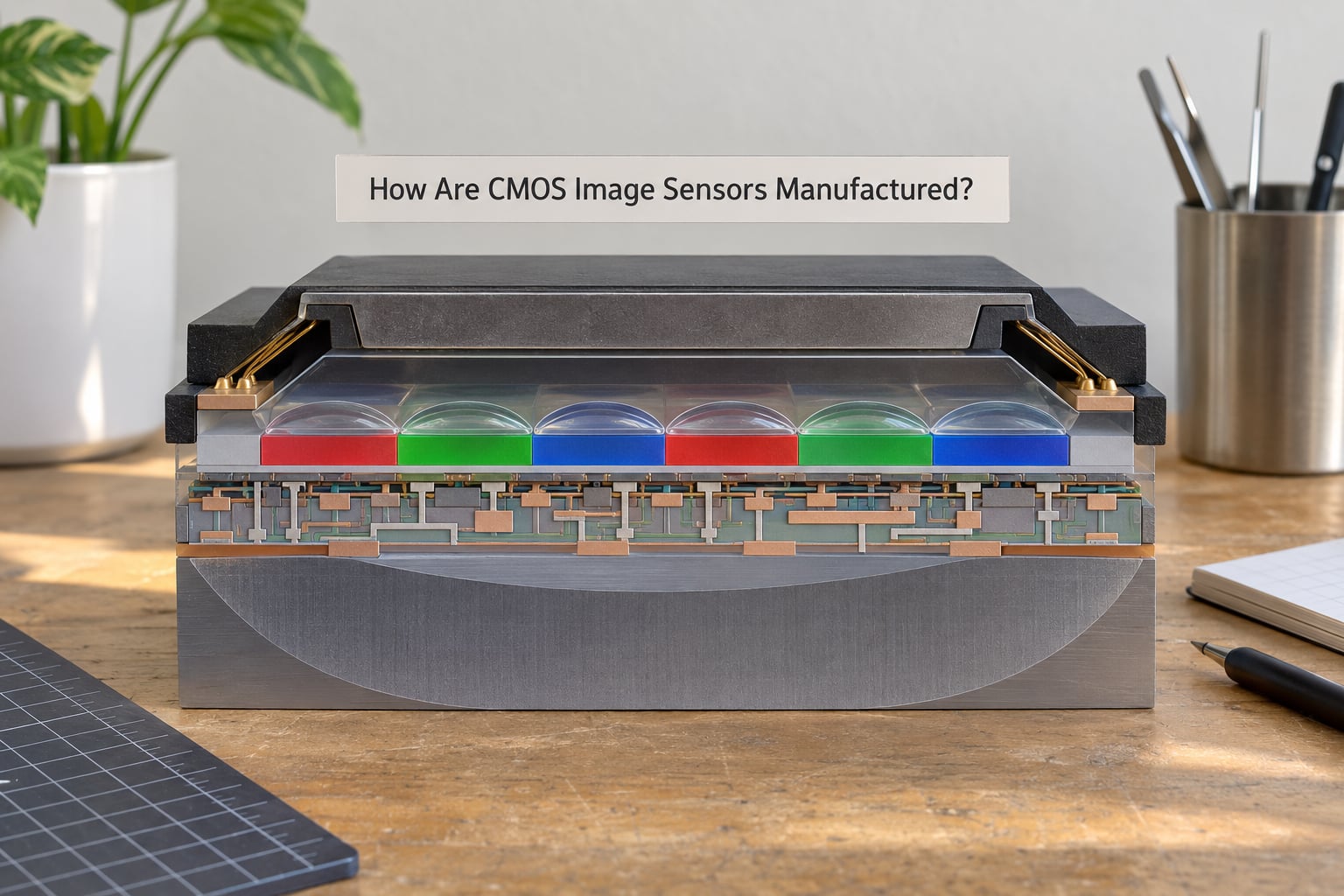
Image sensor manufacturing runs on two wafers that meet in the middle. The pixel wafer carries the photodiodes and pixel transistors, built with an emphasis on light absorption and low leakage. The logic wafer carries the analog-to-digital converters, readout logic, memory and interface, built with an emphasis on speed and density. Logic fabs optimize the opposite way, so splitting them lets each half use its own process.
A modern stacked sensor is assembled front side up: pixel wafer complete, logic wafer complete, then bonded. Copper-to-copper thermocompression bonding is the long-established route, with through-silicon vias carrying signals through the silicon. Hybrid bonding, where oxide surfaces are fused directly at low temperature, achieves finer pitch and has moved into production as pixel sizes shrank.
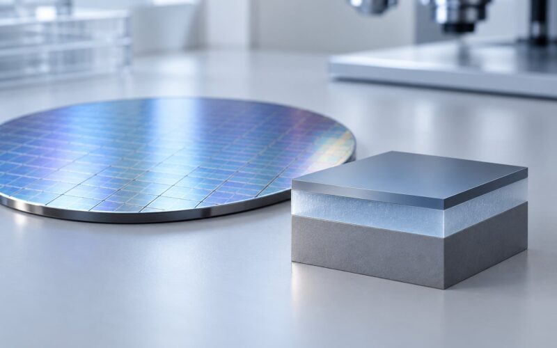
After bonding, the back of the pixel wafer is ground and etched away until a thin silicon film is left, a step called wafer thinning. Now light can enter from the side that has no circuitry on it, which is backside illumination. The thinned backside then gets its own passivation, substrate contacts, a light-shield grid, an aperture opening and a stack of transparent layers, before the color filter array and microlenses go on top.
Frontside-illuminated sensors skip the thinning and the backside modules. They are cheaper and still made, but the metal interconnect sits between the lens and the photodiode, so photons must pass through copper and dielectric before reaching the detector. That costs quantum efficiency and makes wide-aperture designs harder to keep clean.
Every one of these steps runs in a controlled cleanroom. Particles are fatal at this scale, and the process is also constrained by what it cannot tolerate: plasma steps damage the photodiode unless a careful anneal follows, and the optical modules are built after the high-temperature work because the resists and polymers used there cannot survive it.
What Are the Main Steps in the Manufacturing Process?
This is the sequence a process engineer would follow on the floor, module by module. The order of the optical and backside modules changes with architecture, but the flow below describes a current stacked backside-illuminated CMOS image sensor.
Step 1: Wafer start and surface preparation
A prime silicon wafer is cleaned, thermally treated to grow or anneal the interface layer, and inspected. Prime material matters more here than in logic, because a single surface particle landing on a pixel becomes a permanent defect in the finished image.
Step 2: Front-end-of-line device formation
Photolithography and etch build the isolation, the wells, the pinned photodiode and the pixel transistors. This is the front end of line, where the physical device is created. Ion implantation dopes the source, drain and pinning regions, and each implant is followed by an anneal that activates the dopants.
Step 3: Interconnect and logic back end
Metal layers and dielectrics are deposited, patterned and planarized to connect the pixels to their column circuits. Most backend thermal steps in a logic process are far too hot for a photodiode, so the sensor flow is tuned downward, which is one reason a sensor does not simply ride a logic recipe.
Step 4: Logic wafer fabrication
In parallel, a separate wafer goes through a more aggressive logic flow to build the analog-to-digital converters, readout circuitry and interface. The node is usually ahead of the pixel process, and the mismatch is the reason the two wafers exist at all.
Step 5: Wafer bonding
The pixel wafer is aligned to the logic wafer and joined, either by copper thermocompression through vias or by hybrid bonding of oxide surfaces. Alignment tolerance is measured in microns, and voids or particles trapped at the interface show up later as dead columns.
Step 6: Wafer thinning and backside processing
The back of the pixel wafer is ground and dry-etched down to a film thin enough to let light through without spreading. A backside passivation layer is deposited, then substrate contacts are opened so the light-shield grid can be tied to a defined potential.
Step 7: Light-shield and aperture grid
A barrier stack of titanium and titanium nitride is deposited conformally over the backside, then filled with a bulk grid metal such as tungsten. The grid is patterned to form the aperture that defines each pixel’s opening. Pinholes in the barrier or metal diffusion into the silicon are a classic source of hot pixels.
Step 8: Optical clear layers
Two transparent layers are deposited and patterned over the grid, a lower and an upper layer, to build a smooth, low-refraction path toward the filter and lens. Their thickness and sidewall profile set the color-filter thickness uniformity that follows, and therefore the pixel-to-pixel response.
Step 9: Color filter array formation
The mosaic is printed or deposited directly above the pixel, aligned so each filter element lands over one aperture. Black material surrounds each element to absorb stray light, and the alignment tolerance here sets how much crosstalk you get at wide apertures.
Step 10: Microlens formation
A reflow or replica step rounds a resist layer into one lens per photosite. Lens height and curvature are tuned against the filter stack so light is funneled into the active area, recovering the fill factor that the metal interconnect took away.
Step 11: Dicing and package assembly
The wafer is diced, and good dies are mounted on a glass interposer or organic substrate, with the optical side protected by a cover. Wire bond or flip-chip connections bring power, control and the high-speed data interface out of the package.
Step 12: Wafer sort and final test
Before dicing, known-good-die sort screens every die electrically and, on modern lines, optically. Dies that pass are binned by measured performance, and the survivors go into modules with a lens attached, actuators, and the alignment that turns a sensor into a camera module.
| Module | What happens | Typical equipment class |
|---|---|---|
| Wafer start | Cleaning, thermal treatment, inspection | Wet clean, anneal, defect inspection |
| Device formation | Photolithography, etch, implant, anneal | Stepper and scanner, dry etch, implanter |
| Interconnect | Metal and dielectric deposition, patterning, planarization | PVD and ALD, CVD, CMP |
| Bonding | Pixel wafer joined to logic wafer | Thermocompression or hybrid bonder |
| Backside process | Grinding, thinning, passivation, grid fill | Grinder, etcher, PVD, ALD, CVD |
| Optics on die | Clear layers, color filter array, microlens | Coater, lithography, reflow oven |
| Test and package | Sort, dice, mount, wire bond or flip chip | Probe card, test handler, die bonder |
How Are Color Filters and Micro-Lenses Made?
The color filter array is the layer that turns a monochrome photosite array into a color sensor, and it has three common builds. Pigment-based resists carry the dye inside a polymer matrix and are patterned with photolithography. Dye-resist systems use a photosensitive dye that is exposed and developed. Sputtered or evaporated filters build solid dielectric stacks, which give the sharpest spectral edges but are slow and expensive at full-wafer scale.
Most production sensors put the filters over the photodiode, sometimes under the microlens and sometimes over it. Placing them on the diode lets the light-shield grid sit closer to the surface, which tightens optical crosstalk between neighbors. Putting them above the lens can simplify alignment at the cost of a taller optical stack.
Black material surrounds each color element in nearly every design. It blocks light that scatters off the interconnect into the wrong photosite, and a patterned black layer on the microlens surface can do the same job for off-axis light in a wide-aperture lens. In both cases the pattern has to line up with the grid beneath it, which makes this one of the least forgiving alignment steps in the flow.
The microlenses form after the filters. A photosensitive or reflowable resist is coated, patterned over every photosite, and heated so it rounds into a dome. A replica approach copies that dome into a permanent material for better uniformity across a 200-megapixel die. The lens height is then tuned so the light cone entering through the aperture focuses inside the active area rather than on the walls.
Alignment, lens height and stack design all show up in the finished image. Misset the array and you get color shading. Make the lenses too tall and focus shifts at the frame edge. Stack the clear layers badly and you get pixel-to-pixel response variation, which is fixed-pattern noise no amount of downstream processing removes cleanly.
What Does Binning Mean in Image Sensor Production?
Binning is the sorting step that turns one wafer into several product grades. It happens three times: at wafer level before dicing, at die level after packaging, and at module level after the lens is attached. A sensor that fails the first test never gets a package, and one that drifts during module assembly gets rejected later.
Wafer-level test measures what can be reached electrically. Dark current at a set temperature and exposure time, read noise, full-well capacity and linearity, response uniformity across the array, and the count of stuck or dead pixels. Optical test on the line measures what a camera would see: lens shading response, dead column position, and the flat-field signature that reveals a malformed filter or a damaged microlens.
Those numbers map to grades. Dies with low dark current and tight uniformity become the top bin for high-end camera work. Dies with a higher defect count or a wider noise spread can be sold for surveillance or machine vision, where a few bad pixels can be masked in software. Dies that fall outside every product specification are scrap, and on large dies that scrap is expensive.
Module-level test adds variables the fab cannot see. Cover glass flatness, lens-to-sensor spacing, actuator alignment and the tilt between the lens and the die all change the result, so a sensor that passed wafer sort can still fail the corner-sharpness check. That is why image sensor binning data is one of the most useful documents an integrator can get from a supplier.
Why Do Sensor Size and Pixel Design Matter?
Pixel pitch sets the resolution ceiling for a given die, and die size sets the manufacturing economics. Smaller pixels collect fewer photons, so each one needs a wider microlens and a thinner, more transparent interconnect stack above it to recover fill factor. That pressure is what drove the shift from frontside to backside illumination and then to stacked architectures.
Transistor count per pixel is the other lever. A three-transistor pixel is the simplest and gives the most area to the photodiode. Four- and five-transistor pixels add charge holding or splitting capability for high dynamic range, and they cost photosite area. Global shutter needs still more, because the charge has to be stored somewhere while the rest of the frame is read, which is why global sensors trade resolution for motion fidelity and stay in industrial and automotive tiers.
Stacked designs relieve the squeeze. With the pixel transistors on one wafer and the analog-to-digital converters on another, the logic can shrink to a 40-nanometer-class node or finer while the pixel pitch keeps falling. The trade is yield: two wafers, one bond, and a defect in either half can kill an expensive assembly. Pitches below one micron, around 0.56 micron in leading parts, also push deposition step coverage to its limit, which is where atomic layer deposition replaces physical vapor deposition in the barrier and liner steps.
How Does a Foundry Produce a Complete Camera Sensor?
Nobody does the whole chain. A sensor designer specifies the pixel and logic architecture, a foundry or in-house fab builds the wafers, a packaging house assembles the optical package, a module maker adds the lens and actuators, and the camera manufacturer does the final calibration. The die, the sensor package and the camera module are three different things with three different suppliers, and confusing them is the most common sourcing mistake integrators make.
The major sensor makers are Sony Semiconductor, onsemi, OmniVision under Will Semiconductor, Samsung and Canon. Sony is the largest and has pushed stacked backside-illuminated designs furthest. Canon builds in-house for its own cameras. Sony and TSMC operate a joint venture fab in Japan, which is a useful example of the general pattern: image sensor firms with design expertise increasingly partner with foundry capacity rather than owning every tool.
Tooling overlaps heavily with leading-edge logic. Practitioners on camera forums consistently name Applied Materials, Lam Research and Nikon among the vendors that matter for imaging sensors specifically, alongside lithography optics from the major optics makers and inspection and metrology from the defect-detection suppliers. Wafer handling, grinding, bonding and dicing have their own specialist vendors, and bonding is where most of the recent capital spending has gone.
On the supply side, the modules still come from a smaller circle of optical houses. Whoever bonds the wafer, someone else has to grind it, another has to coat the color filters, and a lens supplier has to deliver glass that holds its tolerance across temperature. The chain has more single-source positions than a logic supply chain, which is the practical reason qualification takes months.
What Are the Main Manufacturing Challenges?
Contamination comes first. A particle that lands on the die during bonding, coating or dicing becomes a dead column, and with tens of millions of pixels per die the defect budget is unforgiving. This is why sensors are handled in low-particle environments through the back end, not just in the cleanroom where the transistors were made.
Overlay and alignment follow. Every layer in the optical stack has to land on top of the one below it, and the cumulative error across the grid, the clear layers, the color elements and the lenses sets both the crosstalk and the color uniformity. Wafer curvature after bonding makes this harder than the same step on a flat logic wafer.
Noise has two very different sources. Dark current comes from the photodiode and from leakage through the barrier and the grid: pinholes in the titanium nitride barrier, or tungsten diffusing into the active silicon, both produce pixels that glow in a dark frame. Fixed-pattern noise comes from geometry, mostly an aperture grid that varies across the die. A floating grid with no path to ground adds a slower failure that looks like ghosting.
Yield and cost follow from die size. A full-frame sensor is a large die with a large optical aperture, so both random defect rates and edge-of-lens shading matter more than they do on a small die. Mask sets, design time and test time are fixed costs, which is why a niche part with low volume costs proportionally more per unit than a high-volume part of the same die area. The question of why two sensors of identical area differ so much in price comes up constantly among engineers, and the honest answer is that both manufacturing and market structure are part of it. The r/chipdesign thread that ranks high for this question is blunt about the fixed-cost side for niche parts.
How Do You Choose a Manufacturing Process for an Image Sensor?
Start with the application, because it constrains everything else. A machine vision system that reads a moving part cares about global shutter and predictable latency. A security camera cares about low light and cost per channel. A phone main camera cares about resolution, autofocus and power in a package a few millimeters thick. Automotive work adds temperature range, vibration and a decade-long supply commitment.
From there, the practical framework has seven inputs: required resolution and optical format, pixel architecture and pitch, the readout and ADC placement, optical stack requirements, the performance targets for noise and dynamic range, the lifetime volume, and the supply chain you are willing to qualify.
| Criterion | Mature flow | Advanced flow |
|---|---|---|
| Logic node | Older node, larger transistors | Finer node, faster readout and more on-chip processing |
| Pixel pitch | Roomier, higher fill factor per pixel | Below one micron, needs taller microlenses and tighter barriers |
| Strength | Better yield, cheaper die, easier supply | Lower power, more logic per die, smaller package |
| Weakness | Less logic area limits on-chip HDR and AI | Higher cost, more complex bonding, tighter alignment tolerance |
| Good fit | Industrial, automotive, surveillance volume | Mobile and machine vision where area and power dominate |
A smaller node does not automatically give a better sensor. The pixel layer barely benefits from logic scaling, and the gain has to be paid for in bonding complexity, yield and mask cost. Plenty of successful designs sit on the mature flow because the application never needed the extra logic. The right question is not which node is newest but which node lets the readout do what the system requires within its power and area budget.
The last input is volume, and it is the one that quietly decides most projects. High volume rewards a dedicated process and a custom design. Low volume rewards reusing an existing sensor platform, because mask sets and design time do not shrink with your order quantity.
Frequently Asked Questions
What process is used to manufacture image sensors?
Most modern sensors are made with a CMOS process built around a two-wafer stacked architecture. One wafer carries the photodiode and pixel transistors, a second carries the analog-to-digital converters and readout logic on a more advanced node, and the two are wafer-bonded together. The bonded stack is thinned from the back, given a light-shield grid and clear layers, then coated with a color filter array and microlenses.
Are image sensors made using the same process as computer chips?
The same tools and many of the same modules, but not the same recipe. Sensors run at lower backend temperatures because high heat degrades photodiodes, and they add modules a logic fab does not need, including wafer bonding, backside thinning, grid fill, color filter coating and microlens formation. Dies are also much larger and far more sensitive to single defects, so the defect targets per die are tighter than in logic.
What causes dead pixels in CMOS image sensors?
Dead pixels usually trace to a defect that was already present in the finished die. Common culprits are pinholes in the backside barrier layer, grid metal diffusing into the active silicon, particles trapped during wafer bonding or dicing, and photolithography defects in the photodiode itself. Dark current, not absence of signal, is what usually reveals them in test, which is why dark-frame inspection is part of wafer sort.
How is a finished image sensor tested?
Testing happens at three stages. Wafer sort probes each die electrically and optically before dicing, measuring dark current, read noise, full-well capacity, response uniformity and dead pixel counts. Die-level test repeats key measurements after packaging. Module-level test then checks the assembled camera with its lens, covering lens shading, corner sharpness and focus, which are failures no bare-die test can catch.
Can a semiconductor foundry manufacture image sensors?
Yes, though not every foundry takes on the optical work. The transistor and interconnect part is standard CMOS capability, and foundries build pixel wafers and logic wafers for external sensor designers. The bonding, thinning, color filter and microlens modules need dedicated equipment and process know-how, so those steps often sit with the sensor company or a specialist partner rather than the general-purpose foundry.
Why do image sensors not always use the newest process node?
Because the pixel layer gains little from logic scaling, while the extra bonding steps that a fine node encourages add cost and yield risk. The photodiode is a light-absorbing device, and its performance depends on implant profile, junction depth and low-temperature anneals, not on transistor density. Many sensors ship on mature logic nodes because the readout needs no more, and the savings go into die area and sensitivity instead.
If you are specifying a sensor, start with the binning data and the test conditions behind it. Dark current at a stated temperature, the guaranteed pixel count at a stated illumination, and the noise distribution across the die tell you more about the manufacturing process than the headline pixel count does.
Once that is clear, the architecture question follows quickly: whether the pixel and logic wafers are stacked, whether the sensor is backside illuminated, and where the analog-to-digital converters sit. Those three choices explain most of the differences in sensitivity, power and cost between otherwise similar sensors on the market today.