Power semiconductor basics for beginners come down to one idea: these devices are the electronic switches that let us change electricity from one form into another without wasting most of it as heat. Everything else, the device families, the ratings, the losses, is detail hanging off that one job.
In your phone charger, the grid feed into a factory motor drive, the inverter on a rooftop solar array, and the traction drive of an electric car, power semiconductors chop up, redirect, and switch current at speeds and voltages a signal-level transistor would simply melt at. If you can hold two ideas at once, that a power device is a controlled switch, and that every watt it wastes while switching becomes heat, you already understand the part that trips up most newcomers.
This guide builds from there. It walks through the main device families, maps them to the jobs they actually do, decodes the datasheet terms you will meet first, and ends with a selection checklist you can use the next time you have to pick a device.
Table of Contents
- What Is a Power Semiconductor?
- How Do Power Semiconductors Work?
- Conduction and blocking
- Switching transitions
- Two losses, one design trade
- Soft switching and hard switching
- What Are the Main Types of Power Semiconductors?
- The diode
- The bipolar junction transistor
- The thyristor family
- The MOSFET
- The IGBT
- Wide-bandgap devices: silicon carbide and gallium nitride
- Device family comparison
- IGBT vs MOSFET: the comparison beginners ask for most
- Which Power Semiconductor Is Used Where?
- What Specifications Should Beginners Understand?
- Power semiconductor basics for beginners: the specs that decide everything
- Acronyms you will meet in the first week
- How Do Engineers Choose a Power Semiconductor?
- Why Do Thermal Design and Layout Matter?
- Power Semiconductor Basics for Beginners: Frequently Asked Questions
- What are the basics of power electronics?
- What are 10 examples of power semiconductor devices?
- What is an IGBT and a MOSFET?
- How do you choose the right power semiconductor?
- Why are gate resistors used when driving a MOSFET?
- Is there a free course in power electronics available?
- Conclusion
What Is a Power Semiconductor?
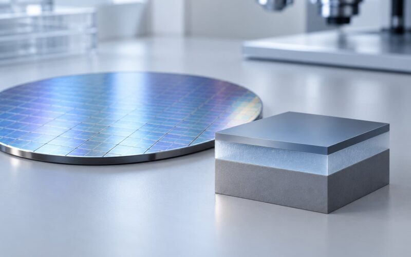
A power semiconductor is a specially engineered switching device, built from silicon or a wide-bandgap material such as silicon carbide, designed to block high voltages and carry high currents while losing as little energy as possible. In short: it is a voltage-controlled valve in the path of electrical power.
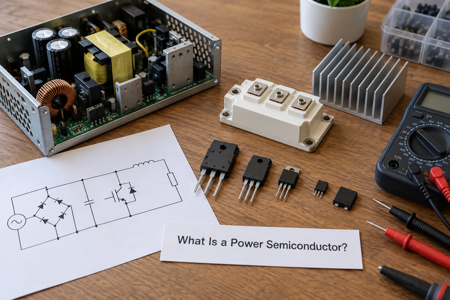
What separates a power semiconductor from an ordinary signal transistor is the ratio of what it has to survive to how little it is allowed to waste. A signal transistor in a radio might handle a volt and a few milliamps. A power device in a solar inverter blocks hundreds of volts, switches tens or hundreds of amps, and still has to keep its losses low enough that a heat sink stays a sensible size.
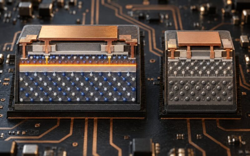
That demand changes the physics of the chip. Power devices are usually built vertically, with the resistive path running from the top terminal to the bottom terminal, so heat can leave through the package. Low-voltage logic chips are built flat, optimised for speed and density rather than for moving kilowatts around.
Power electronics is the field built on these devices: the study of circuits that convert, control, and condition electrical energy. Almost every converter, charger, and drive you will ever open up is a chain of these switches with passive components doing the smoothing, and understanding the chain is what makes the device datasheets readable.
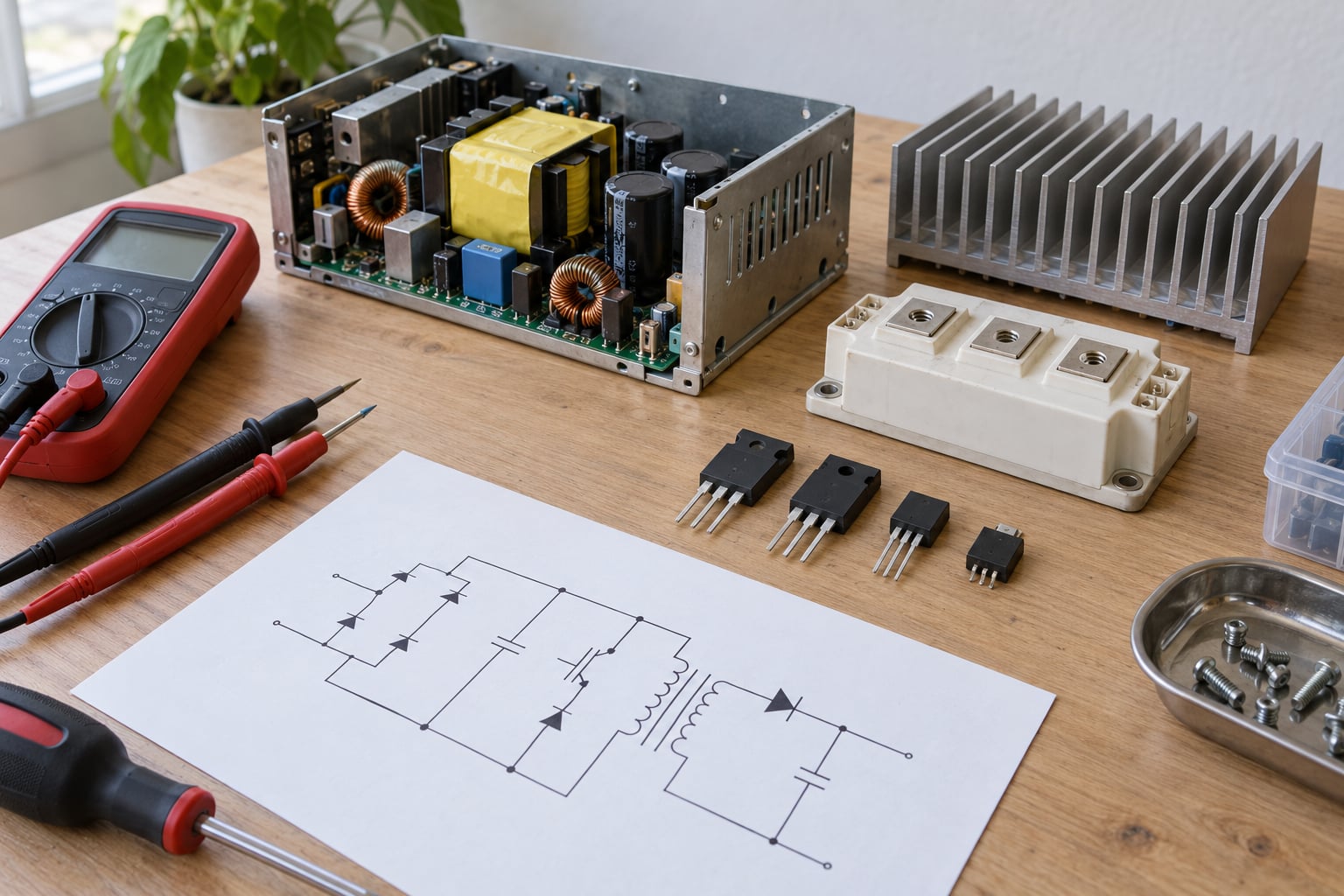
Within almost any converter, the semiconductors occupy a predictable set of positions. In a switch-mode power supply, an AC input hits a rectifier, which turns AC into rough DC. A switching stage then chops that DC at high frequency, an inductor and capacitor filter it, and a control loop adjusts the duty cycle to hold the output where it is supposed to be. The semiconductors do the chopping; the passive components do the smoothing.
It helps to think of the whole chain as input, conversion, output. Once you can point at a block on a block diagram and name the device inside it, datasheets stop being intimidating.
How Do Power Semiconductors Work?
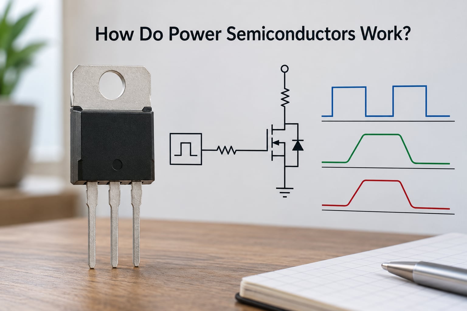
Power semiconductors work as controllable electronic switches: a control signal sets them into a conducting state that passes current, or a blocking state that stops it. Voltage-driven families such as MOSFETs and IGBTs use the voltage on a gate, while current-driven families such as BJTs and thyristors need current driven into a terminal to stay on.
Conduction and blocking
A device in its on state still has some resistance or some forward drop. That leftover is the conduction loss, and it shows up as heat. For a MOSFET the loss is current squared times RDS(on), which is why on-state resistance is one of the first numbers a designer looks at.
A bipolar device such as an IGBT or a thyristor behaves differently. It is described by a saturation voltage, VCE(sat), typically a couple of volts, so the conduction loss is roughly that voltage times the current. The two descriptions are equivalent; they are just different ways of expressing the same wasted energy.
Blocking is the other side of the job. A device rated at 650 V can hold off 650 V with essentially no current flowing, provided the voltage is applied across the correct terminals. The rating is a promise made at a specific case temperature, and it is not a number to lean on continuously.
Switching transitions
Real switching is not instantaneous. Voltage across the device and current through it trade places over a short window, and the area under both curves during that window is energy that never reached the load. That is the switching loss.
Turn-on loss is dominated by the current that must build while the voltage is still falling. Turn-off loss is dominated by the voltage that builds while the current is still falling. Higher switching frequency means more of these transitions every second, so switching loss scales roughly with frequency, and fast-switching devices get hot quickly even when they are barely conducting.
Gate charge, measured in nanocoulombs, describes how much charge the control terminal needs before the device actually changes state. A device with high gate charge driven by a weak driver does not switch cleanly, and the partially-switched time turns straight into heat.
Two losses, one design trade
Which loss dominates depends on how long the device spends conducting. A device that is on almost all the time loses mostly in conduction. A device that is on for short pulses at high frequency loses mostly in switching.
That is the whole reason both MOSFETs and IGBTs exist. IGBTs carry current efficiently, so they win in a 50 Hz motor drive where each transistor conducts for roughly half a cycle. MOSFETs switch quickly, so they win in a laptop power supply running at hundreds of kilohertz. Voltage-driven versus current-driven is not academic; it decides which device family is even a candidate.
Soft switching and hard switching
In hard switching, a device snaps between its two states at full voltage and current. In soft switching, the circuit is arranged so the transition happens at low voltage, at low current, or both, which slashes switching loss. Soft switching needs extra components, usually resonant inductors and capacitors, to make that happen.
Beginners often meet continuous and discontinuous conduction mode at the same time. In continuous conduction mode, the inductor current in a converter never falls to zero. In discontinuous conduction mode it does, briefly, every cycle. The mode changes the control design but not the fundamental role of the switching device.
What Are the Main Types of Power Semiconductors?
The main types of power semiconductor devices fall into four broad groups by construction: unipolar devices such as diodes and MOSFETs, bipolar devices such as BJTs and IGBTs, thyristor-family devices, and wide-bandgap devices. Every power device you will meet is a variation on one of these, and knowing which group a part belongs to tells you how it will behave in a circuit.
The diode
The power diode is the simplest device and the right starting point. It conducts current in one direction and blocks it in the other, with a forward voltage drop that rises with temperature. It has no control terminal, so you cannot switch it on demand; it does whatever the circuit demands.
That passivity is a strength in a rectifier, where you want conversion with no control effort. It is a weakness in a chopper, where you need to turn conduction on and off. Power diodes also have a reverse recovery characteristic: when a forward-biased diode is switched off, stored charge has to clear, producing a current spike. The reverse recovery time, trr, is the number to check when the diode sits across a fast switching node.
The bipolar junction transistor
A power BJT is a current-driven device. Base current has to keep flowing for the transistor to stay on, and a significant share of that current is wasted in the drive itself. Power BJTs are now mostly a historical family outside a few very high voltage, very high current niches, but they still appear in old textbooks because they explain the bipolar principle so cleanly.
The thyristor family
An SCR, the Silicon Controlled Rectifier, is a four-layer p-n-p-n device with three terminals: anode, cathode, and gate. A pulse to the gate latches it on, and once latched it stays on until the current through it drops below the holding current. That behaviour is exactly what you want in a phase-controlled rectifier, where the gate pulse sets the firing angle and the AC cycle turns the device off for you.
A TRIAC is the bidirectional version, used to control both halves of an AC waveform. A DIAC is its trigger partner: a small two-terminal device that breaks down and conducts a pulse of current when the voltage across it crosses a threshold, which is what starts the TRIAC.
Thyristors are the oldest power family still in heavy use, because they handle enormous voltages and currents and fail shorted rather than open, which is the safer behaviour in high-energy systems. Their limitation is switching speed, since they cannot be turned off by a control signal.
The MOSFET
A power MOSFET is voltage-driven, which means the steady-state gate current is essentially zero and the drive circuit stays simple. It switches fast, it parallelises well, and its main weakness is a rising on-state resistance as the die shrinks and as the temperature climbs.
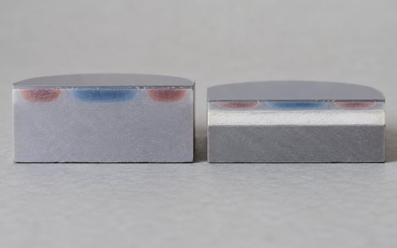
Two structural ideas explain modern MOSFETs. Super-junction or super-MOS devices use a tailored epitaxial drift region to push RDS(on) far below what a plain vertical structure allows. Punch-through and non-punch-through structures trade on-resistance against the voltage the drift layer can block. A vertical structure with a field-stop layer near the substrate lets the die be made thinner, which reduces resistance while keeping the blocking capability.
Every power MOSFET contains a body diode, a parasitic p-n junction formed by its own structure. That diode carries current when the device is off and in most modern silicon MOSFETs has a forward drop of roughly 0.7 to 0.9 V, which is high compared to a fast rectifier diode. Designers who need a lower drop select a co-packaged external diode.
The IGBT
An IGBT, the insulated-gate bipolar transistor, combines a MOS gate with a bipolar output stage. The gate makes it voltage-driven, which is the main practical advantage over a BJT. Internally, a high-voltage drift region blocks the voltage while a comparatively low-resistance channel carries the current, so a 1200 V IGBT can present about 2 V across itself when fully on.
IGBTs dominate from roughly 600 V to 1700 V and above, in motor drives, solar inverters, and traction inverters, because they combine blocking voltage with low conduction loss. Their trade is speed: tail current extends the turn-off transition, so IGBTs do not like switching frequencies in the hundreds of kilohertz.
Variants exist for specific problems. RC-IGBTs use a resistor across the gate to trade speed against loss. IEGTs change the carrier distribution so the collector current falls more sharply, which suits high-power inverters. Punch-through IGBTs use a thinner drift region than non-punch-through types, giving lower conduction voltage at the cost of a higher tail.
Wide-bandgap devices: silicon carbide and gallium nitride
Wide-bandgap semiconductor materials have a larger energy gap between the valence and conduction bands than silicon, which allows a given field to be sustained with less heat, faster switching, or both. Silicon carbide is the practical choice for high voltage, high current work. Gallium nitride is the practical choice for lower voltages at very high frequency.
Both are harder to make and more expensive per unit than silicon, and neither is cheaper for a 24 V buck converter. The trade is worth it when switching frequency, power density, or operating temperature is the binding constraint, which is why they show up in EV traction inverters, fast chargers, solar inverters, and data centre power supplies.
Device family comparison
| Device | Control | Typical voltage | Switching speed | Strength | Limitation | Common use |
|---|---|---|---|---|---|---|
| Power diode | None | 50 V to thousands | Limited by trr | Simple, cheap, rugged | Not controllable | Rectifiers, freewheel paths |
| Power BJT | Base current | 100 V to 1000 V | Moderate | High current capability | Continuous base drive, slow | Legacy high-power drives |
| SCR thyristor | Gate pulse, latching | 200 V to 6500 V | Slow | Blocks enormous voltage, fails shorted | Cannot be gated off | HVDC, phase-controlled rectifiers, inverters |
| TRIAC | Gate pulse | 200 V to 1000 V | Slow | Switches both AC halves | Cannot be gated off | Dimming, motor speed control, heating |
| Power MOSFET | Gate voltage | 20 V to 900 V | Very fast | Low gate current, easy paralleling | On-resistance rises with temperature | DC-DC converters, SMPS, low-voltage DC |
| IGBT | Gate voltage | 600 V to 6500 V | Medium | Low conduction loss at high voltage | Tail current limits frequency | Motor drives, solar, EV traction, inverters |
| SiC MOSFET | Gate voltage | 650 V to 3300 V | Very fast | Low loss, high temperature, no reverse recovery | Cost, gate drive requirements | Traction, solar string inverters, fast chargers |
| GaN FET | Gate voltage | 30 V to 650 V | Extremely fast | Very low switching loss at high frequency | Short-circuit withstand time is short | Phone and laptop chargers, data centre supplies |
IGBT vs MOSFET: the comparison beginners ask for most
Both a MOSFET and an IGBT are turned on by a positive voltage on the gate, but they behave differently under load. A MOSFET conducts like a resistor, so its loss grows as the square of current, while an IGBT behaves like a forward-biased junction with a roughly fixed drop of about 2 V when saturated.
The crossover sits around a few hundred volts. Below roughly 600 V, MOSFET on-resistance and switching speed win. Above that, IGBT conduction loss wins by a widening margin, until the required frequency becomes high enough that the IGBT tail current dominates.
| Parameter | Power MOSFET | IGBT |
|---|---|---|
| On-state behaviour | Resistive, described by RDS(on) | Forward-biased, described by VCE(sat) |
| Conduction loss at high current | Rises steeply with current | Rises roughly linearly with current |
| Switching speed | Very fast, tens to hundreds of kHz and beyond | Moderate, typically hundreds of Hz to tens of kHz |
| Tail current at turn-off | Negligible | Significant, dominates switching loss at high frequency |
| Gate drive current | Peak only, then near zero | Peak only, then near zero |
| Body diode | Present, with a relatively high forward drop | Absent, so a separate freewheel diode is usually fitted |
| Typical voltage class | 20 V to 900 V | 600 V to 6500 V |
| Paralleling for more current | Easy, matched RDS(on) helps | Possible, but current sharing is less forgiving |
Which Power Semiconductor Is Used Where?
No device is best at everything. The right choice for a given job follows from four questions: what voltage, what current, what switching frequency, and how much heat can the assembly shed. Match those four against the device table above and the answer usually narrows to one or two families.
Rectifiers and freewheel paths use power diodes, and increasingly fast recovery or SiC diodes where the reverse recovery spike matters. A classic exercise is the half-wave rectifier: a single diode passes the positive half of an AC waveform, and a load resistor plus smoothing capacitor turns the pulsating output into something closer to DC. Adding a second diode in a bridge configuration gives full-wave output with more ripple reduction. None of this needs a control signal, which is exactly why diodes are used for the first stage of nearly every power supply.
DC-DC converters in laptops, servers, phones, and battery systems run at tens to hundreds of kilohertz. Their switches are almost always MOSFETs, because switching loss is the dominant term and the voltages involved are low. A synchronous buck converter replaces the rectifier diode with a second MOSFET, so the inductor sees low loss on both halves of the cycle.
Motor drives and industrial inverters sit in a different regime. A drive running at a few hundred hertz needs a device that blocks high voltage and conducts large current cheaply rather than switching fast. That is IGBT territory, and it is why industrial drive cabinets are full of them. Newer high-efficiency drives use SiC modules in the same position.
Solar inverters, wind converters, and grid-tied storage inverters are effectively the same machine as an industrial drive with a different load profile: hundreds of volts DC in, AC out, switching in the tens of kilohertz. IGBTs dominate the installed base, with SiC modules increasingly used in new designs to raise efficiency and simplify filtering.
EV traction inverters sit at the high end of the same requirement, several hundred kilowatts switched at a few kilohertz, and the move to SiC there is well under way because of how much it reduces cooling mass. EV charging stations add a DC fast path that switches at tens to hundreds of kilohertz, a frequency where MOSFETs and GaN devices start to make more sense than silicon IGBTs.
Power factor correction stages sit at the front end of three-phase supplies and run in boost or active rectifier configurations, usually with silicon MOSFETs or IGBTs depending on power. Small consumer power supplies, LED drivers, and appliance controls are where you will find the widest range: a low-voltage synchronous buck with small MOSFETs in a laptop, a boost converter in an LED driver, a TRIAC phase controller in a dimmer.
HVDC transmission and large motor drives at megawatt scale use press-packed thyristors, because nothing else blocks that voltage reliably and a shorted device is a contained fault there. The same reason makes thyristors the standard in high-power inverter stacks.
One more category shows up in almost every modern design: modules and intelligent power modules. A power module packages several dies, their busbars, and often gate drivers into a single assembly, cutting the parasitic inductance that switching layouts cannot tolerate. An intelligent power module adds the driver, sometimes current sensing and protection, and fault reporting. Both exist to solve the same problem: a few excellent dies wired badly is worse than a few average dies wired well.
What Specifications Should Beginners Understand?
Power semiconductor datasheets look intimidating because they list dozens of parameters, but a beginner only needs a dozen to make a first judgement. The table below covers those, in plain language, with the reason each one matters.
Power semiconductor basics for beginners: the specs that decide everything
| Specification | What it means | Why it matters |
|---|---|---|
| Blocking voltage (VDS, VCE, VRRM) | Maximum voltage the device can hold off with negligible leakage | Sets the voltage class; derating is required for transients |
| Continuous drain or collector current | Current the device can carry indefinitely at a stated case temperature | Constrains steady-state thermal design more than the switch itself |
| Pulsed current | Short-duration current allowed, with a duty and pulse width limit | Covers inrush and overload conditions, not steady state |
| RDS(on) | On-state resistance, specified at a test gate voltage and temperature | Drives conduction loss; rises with junction temperature |
| VCE(sat) | Voltage across a saturated IGBT at a rated current | The conduction loss figure for bipolar devices |
| Switching loss (Eon, Eoff) | Energy dissipated per switching transition | Multiply by switching frequency to get average switching loss |
| Gate threshold VGS(th) | Gate voltage at which the device begins to conduct appreciably | A drive target, not a guarantee; a device just above threshold is hot |
| Total gate charge Qg | Charge needed to swing the gate from off to on | Determines how hard the driver must work and how fast the switch can move |
| Body diode and trr | Free-wheeling path and its reverse recovery time | A high trr diode adds loss and a spike across the switching node |
| Junction temperature rating | Maximum temperature at the die, e.g. 150 °C or 175 °C | The real ceiling on power density |
| Thermal resistance junction-to-case | Temperature rise per watt from die to case | Determines the size of heat sink needed |
| Safe operating area (SOA) | Region of voltage and current where the device can operate without damage | The curve that tells you what linear-mode operation is allowed |
Two terms cause endless confusion. VGS(th) is the voltage at which the MOSFET starts to conduct, and beginners treat it as a set point. It is not. A MOSFET driven just above its threshold behaves like a resistor in the ohmic region and dissipates badly, so good designs drive the gate to 10 V and rely on RDS(on) specified at that voltage rather than stopping at the threshold.
The safe operating area is a curve, not a number. It shows the combinations of drain voltage and drain current the device can survive for a stated time. Staying inside it is what allows a MOSFET to be used in linear mode for a regulated output, which is otherwise a fast way to destroy one.
Acronyms you will meet in the first week
Acronym density is one of the main reasons beginners bounce off this field. A short glossary removes most of the problem: SCR is a Silicon Controlled Rectifier, a latching four-layer thyristor. TRIAC is the bidirectional thyristor, and DIAC is the two-terminal trigger device that fires it. IGBT is the insulated-gate bipolar transistor, combining a MOS gate with a bipolar output stage. BJT is the bipolar junction transistor, the current-driven predecessor. SOA is the safe operating area, and trr is reverse recovery time. CIB, sometimes seen in older course material, means a converter with an IGBT and its antiparallel diode, and IPM is an intelligent power module, a module with its gate driver and protection circuitry integrated. RDS(on) is the on-state resistance of a MOSFET, and VCE(sat) is the saturation voltage of a bipolar device.
Once those are familiar, datasheets become readable. What remains is mostly curve families, and you can learn them one at a time as the design demands.
How Do Engineers Choose a Power Semiconductor?
Engineers choose a power semiconductor by starting with voltage and current, then working outward through topology, frequency, losses, thermal limits, and packaging. A short numbered process is easier to follow than any single rule, because every family looks plausible until you apply all the constraints in order.
Start with the electrical envelope. Take the highest voltage the device must block, add transient margin for switching spikes and line disturbances, and choose the next voltage class up. Then take the current the device must carry and add thermal margin. Beginners routinely skip this margin step and then wonder why a marginal design failed in a hot enclosure rather than on the bench.
Set the switching frequency next, because it decides which device family is even possible. Below roughly 600 V and above tens of kilohertz, you are looking at MOSFETs. Above 600 V at a few tens of kilohertz, IGBTs. If the voltage is high and the frequency is also high, wide-bandgap is the reason the design exists at all.
Budget the losses, which means conduction loss and switching loss added together and multiplied by the duty cycle. This is where RDS(on) or VCE(sat) pays for itself, and where a quick comparison of two candidate parts is often decisive. Check the datasheet figure at the temperature you expect, not the 25 °C headline, since both parameters degrade with heat.
Then check the thermal path. Compute the junction temperature from the estimated losses and the thermal resistance from the case to the ambient, including the heat sink. If the number comes out near the rating, the design is not finished, it is just optimistic.
After that comes the package and the gate drive. A package has to fit the current, the voltage, and the heat, and the driver has to supply the peak gate current the device needs to switch on the schedule you designed. Mismatched driver strength is a common and expensive mistake.
Cost and reliability come last, and they come together. Higher voltage, higher current, and faster switching ratings all cost more, and a part that sits 10 °C below its rating limit will usually survive longer than one that runs at the limit. The cheapest device that meets the requirements with margin is the correct answer; the cheapest device that technically meets them is a reliability problem waiting for a customer call.
Why Do Thermal Design and Layout Matter?
Electrical ratings alone do not decide whether a power design survives, because every watt of conduction and switching loss leaves the device as heat. If that heat cannot get out, junction temperature climbs until the device degrades or fails, regardless of how well it was rated.
Heat flows from the die to the case, from the case through a thermal interface to the heat sink, and from the sink into the air. Junction-to-case thermal resistance is a property of the package. Case-to-ambient resistance is a property of your design, and beginners are surprised by how much of the total it turns out to be.
A heat sink is sized to move heat at a given temperature rise. Bigger surface area means lower resistance, and finned or extruded shapes beat flat plates for the same volume. Airflow, ambient temperature, and orientation all shift the number, which is why a design that works on a bench in a cool room can fail in a sealed enclosure at 55 °C.
Beyond the sink, three layout choices do a surprising amount of work. First, switching loop inductance: the loop formed by the high-voltage DC link, the switching device, and the low-side device or diode should be as small as physically possible, because every volt-nanosecond of stray inductance in that loop becomes a voltage spike across the device it is meant to protect. Second, gate resistance: a resistor at the gate limits peak drive current, slows the edge, reduces oscillation and EMI, and spreads switching loss across several devices instead of concentrating it in one. Third, copper area: wide tracks and planes on both sides of a board act as a heat spreader, and they also lower parasitic resistance.
Layout symmetry matters too, especially in paralleled devices and in multi-cell modules. If two paralleled MOSFETs do not share current evenly, the weaker one runs hotter, gets weaker, and takes more current, which is a positive feedback loop ending in a failed device. Manufacturers state matching requirements, and following them is not optional.
The short version: build a thermal model early, keep switching loops tight, drive gates with a deliberate resistor, and treat the datasheet’s recommended layout as a starting point rather than a suggestion. Every datasheet thermal rating is quoted for a specific test setup, and your board is not that setup.
Power Semiconductor Basics for Beginners: Frequently Asked Questions
What are the basics of power electronics?
Power electronics is the study of circuits that convert, control, and condition electrical energy using semiconductor switches rather than mechanical or resistive elements. The core toolkit is a rectifier, a switching stage, a filter, and a control loop. Devices used range from power diodes and thyristors to MOSFETs and IGBTs.
What are 10 examples of power semiconductor devices?
Ten common power semiconductor devices are the power diode, Schottky diode, silicon-controlled rectifier (thyristor), TRIAC, DIAC, power BJT, power MOSFET, IGBT, silicon carbide MOSFET, and gallium nitride FET. Each family is optimised for a different voltage, current, and switching-frequency combination, so the application decides which one fits.
What is an IGBT and a MOSFET?
Both are turned on by a positive gate voltage, but they conduct differently. A MOSFET conducts like a resistor described by RDS(on), which makes it fast and efficient at low voltage. An IGBT conducts like a forward-biased junction with a roughly 2 V drop, which makes it efficient at high voltage and high current. Above about 600 V, IGBTs usually win.
How do you choose the right power semiconductor?
Start with the highest blocking voltage and the continuous current, adding transient and thermal margin, then set the switching frequency. That combination usually narrows the family to MOSFET, IGBT, or wide-bandgap. Finally check total losses, junction temperature with your intended heat sink, and whether your gate driver can supply the peak current the device needs.
Why are gate resistors used when driving a MOSFET?
A gate resistor limits the peak gate current, which slows the switching edge and reduces oscillation, ringing, and electromagnetic interference. It also spreads the switching loss across several transistors when devices are paralleled, instead of concentrating it in the fastest one. The value is a compromise, since too much resistance makes the device switch sluggishly and burn more during the transition.
Is there a free course in power electronics available?
There are free and openly available options. University course pages and lecture notes are often published openly, and semiconductor manufacturers including Infineon, onsemi, STMicroelectronics, and Vishay publish free e-learning modules and application notes covering devices, gate drive, and thermal design. Search for the device family plus e-learning or application note rather than for a generic course listing.
Conclusion
Power semiconductor basics for beginners reduce to a small set of ideas worth learning in order. Start with the device as a switch, and with the difference between conduction loss and switching loss. Then meet the families one at a time, so the datasheet numbers behind them stop being abstract.
From there, work through this sequence. First, blocking voltage and continuous current, the two numbers that rule devices in or out. Second, the loss parameters, RDS(on) or VCE(sat) plus switching energy, because those decide how much heat you have to remove. Third, the thermal path, junction temperature, interface, heat sink, and airflow, since that is what turns a rating into a working product. Fourth, datasheet literacy: knowing which curve answers your question and which parameters are quoted at 25 °C anyway. Fifth, applications, working from a half-wave rectifier up to a buck converter, then a DC-DC converter, then a motor drive, since each one adds a single new concept to the last.
What trips beginners is rarely the physics. It is the vocabulary and the assumption that a number printed on page one of a datasheet can be used as-is. Get past those two, and the rest of the field is just careful engineering.