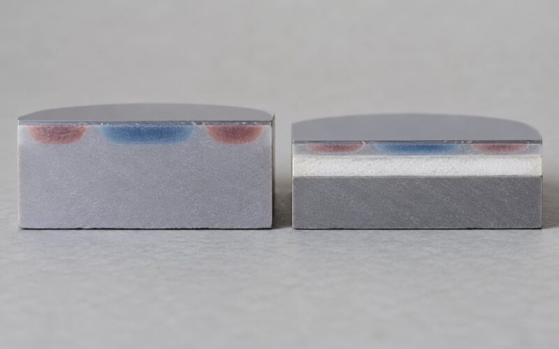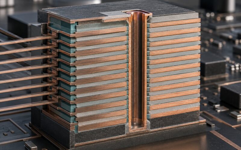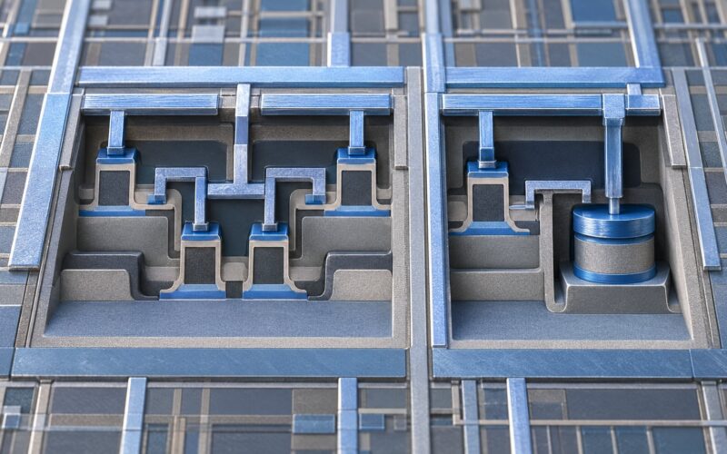
Gallium nitride semiconductors are wide-bandgap devices built from a compound of gallium and nitrogen, and in power conversion they switch faster, block higher voltages and move less heat than silicon. That single material difference is why you now find them inside laptop chargers, data center power supplies, EV fast chargers and 5G base stations. This guide explains the physics behind the material, how the devices are built, where the advantages are real, and where silicon still wins.
Table of Contents
- What Are Gallium Nitride Semiconductors?
- What does wide bandgap semiconductor mean?
- How Gallium Nitride Semiconductors Work
- The two-dimensional electron gas
- How a device blocks and conducts
- What is the GaN HEMT device?
- Why Gallium Nitride Is Different from Silicon
- How Gallium Nitride Semiconductors Are Made
- Who makes GaN chips?
- What Are the Main Advantages of GaN?
- Where Are Gallium Nitride Semiconductors Used?
- EV charging and on-board converters
- Data centres and AI server power delivery
- Consumer adapters and USB-C Power Delivery
- Telecommunications, radar and satellite links
- Lighting, sensing and harsh environments
- What Are the Limitations and Challenges of GaN?
- How Does GaN Compare with Other Semiconductor Materials?
- How Do You Choose a GaN Device?
- Frequently Asked Questions
- Why is gallium nitride used in chargers?
- Will gallium nitride replace silicon?
- Does gallium nitride produce less heat than silicon?
- What is the band gap of gallium nitride?
- Is GaN reliable enough for automotive and safety-critical designs?
- Which countries make gallium nitride chips?
- Key Takeaways
What Are Gallium Nitride Semiconductors?
Gallium nitride (GaN) is a binary III-V compound semiconductor made by combining gallium, a soft grey metal, with nitrogen, a gas. The resulting crystal has a direct bandgap of about 3.4 eV, roughly three times that of silicon, and that wide gap between the valence band and conduction band is the root of nearly every advantage and compromise that follows.
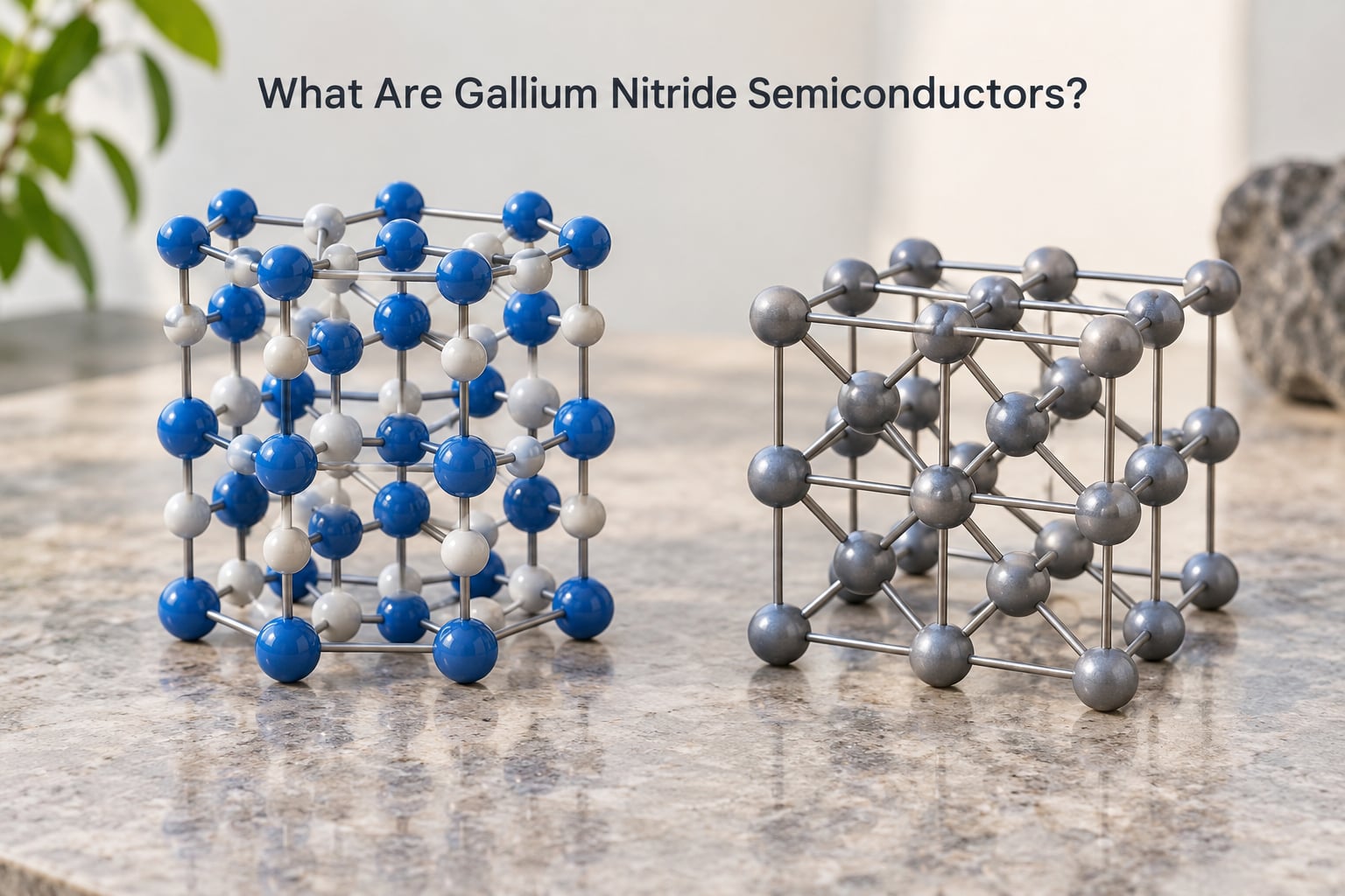
Gallium sits in group 13 of the periodic table, nitrogen in group 15, which is why chemists classify GaN as a III-V compound rather than an elemental semiconductor like pure silicon.
- Crystal structure: bulk GaN adopts the hexagonal wurtzite lattice, a different geometry from the cubic diamond structure of silicon.
- Bandgap: 3.4 eV at room temperature, a direct gap, so electrons can absorb and emit light efficiently.
- Melting point: the compound does not melt so much as decompose at roughly 2500 degrees Celsius, which is why growth happens in vapour-phase reactors.
- Form: single-crystal epitaxial films, not bulk chunks, because the useful electronic behaviour lives in a thin engineered layer.
What does wide bandgap semiconductor mean?
The bandgap is the energy an electron needs to jump out of the valence band, where it is bound, into the conduction band, where it can move freely. Silicon needs about 1.1 eV, gallium arsenide about 1.42 eV, and GaN about 3.4 eV. A wide gap means far more energy has to be supplied before thermal agitation creates unwanted current, and far more electric field has to be applied before the crystal breaks down and conducts destructively.
Two consequences follow directly. The device holds voltage better, so the die can be made thinner and the losses at a given voltage drop are lower. And the device keeps behaving predictably at higher junction temperatures, which matters in a fast charger or a traction inverter.
How Gallium Nitride Semiconductors Work
Every semiconductor switch is really a valve that lets electrons through or stops them. In silicon that valve is set by doping, meaning deliberately adding donor or acceptor atoms so the free-carrier density is predictable. In GaN power transistors, the high-mobility channel is created structurally instead, through the crystal itself.
The two-dimensional electron gas
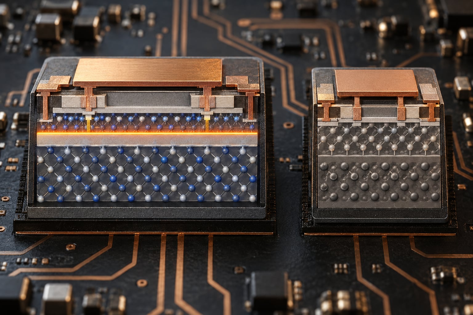
A GaN HEMT stacks aluminium gallium nitride on top of gallium nitride. Where the two materials meet, the differing lattice constants and the built-in electric field of the wurtzite crystal create a polarisation charge that confines a dense sheet of free electrons to a layer only a few nanometres thick. That sheet is the two-dimensional electron gas, or 2DEG.
Confining electrons to two dimensions means very few of them collide with the crystal lattice as they travel, which is why electron mobility in the channel exceeds 1000 cm2/Vs and the saturation velocity is high. The practical analogy is a motorway: the 2DEG is a two-lane road with no junctions, so electrons reach their speed limit quickly and keep it, while bulk conduction is single-lane traffic through a roundabout.
How a device blocks and conducts
The gate terminal controls the 2DEG. Apply a voltage that depletes the channel and the electrons are squeezed out, so the device blocks. Release it and the channel refills, so current flows. Because the blocking behaviour comes from a field rather than from doped junctions, there is no injected minority charge to clear afterwards, which is why GaN devices have almost no reverse recovery charge compared with a silicon MOSFET body diode. In hard-switched topologies such as totem-pole PFC or dual active bridge, that removed loss is a large part of the efficiency gain.
What is the GaN HEMT device?
A GaN HEMT is a high electron mobility transistor: a gate sitting above a 2DEG channel formed at an AlGaN/GaN heterojunction. Two families exist in volume. Depletion-mode devices conduct at zero gate voltage and need a negative gate drive to turn off. Enhancement-mode devices conduct only when the gate is driven positive, and the common implementation is a p-GaN gate layer that makes the device look electrically like a silicon MOSFET, which simplifies gate drive for existing power supply teams.
Why Gallium Nitride Is Different from Silicon
The table below puts the three most-discussed materials side by side. Silicon remains the volume standard, gallium arsenide dominates high-frequency RF, and gallium nitride sits in between on voltage while leading on switching speed.
| Property | Silicon (Si) | Gallium arsenide (GaAs) | Gallium nitride (GaN) |
|---|---|---|---|
| Bandgap | 1.12 eV | 1.42 eV | 3.4 eV |
| Critical breakdown field | about 0.3 MV/cm | about 0.4 MV/cm | about 3.3 MV/cm |
| Electron mobility | about 1400 cm2/Vs | about 8500 cm2/Vs | about 1000 to 2000 cm2/Vs in the 2DEG |
| Thermal conductivity | about 150 W/cm K | about 46 W/cm K | about 1.3 W/cm K |
| Saturation velocity | about 1.0 x 10^7 cm/s | about 1.1 x 10^7 cm/s | about 1.8 x 10^7 cm/s |
| Typical device role | Default switch and analogue device | RF amplifiers, optoelectronics | Fast high-frequency power switching and RF |
The critical breakdown field is the number to remember: it is roughly ten times that of silicon, so a GaN switch can hold the same blocking voltage in a fraction of the die thickness. Less silicon, less resistance, less heat.
Thermal conductivity runs the other way, and it deserves honesty. GaN conducts heat about a hundred times worse than silicon, and practitioners put silicon carbide at 3 to 4 W/cm K against 1.3 to 1.5 W/cm K for GaN. That is why GaN wins below roughly 900 V and silicon carbide takes over in traction inverters and very high voltage systems, and why nearly every GaN design is really a thermal design.
How Gallium Nitride Semiconductors Are Made
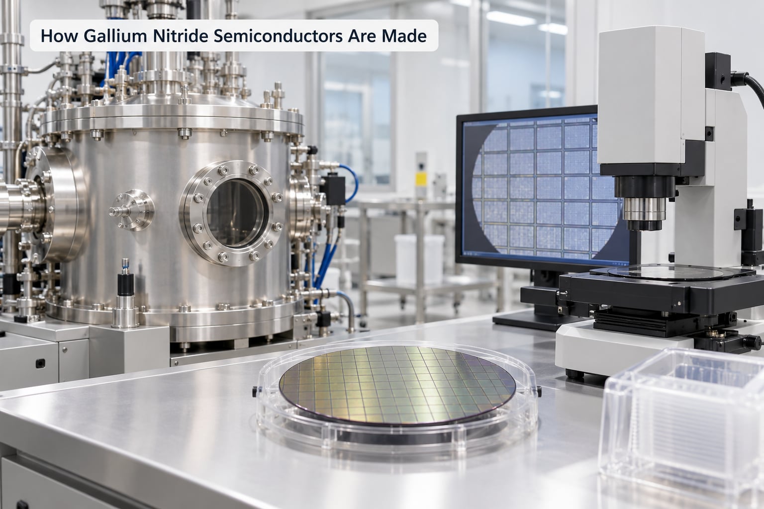
You cannot grow bulk gallium nitride crystals at the sizes industry needs, because it decomposes before it melts. The industry grows thin single-crystal films epitaxially, meaning layer by layer on a substrate that provides the crystal template.
- Substrate choice. Sapphire gives a well-matched crystal and is the workhorse for LEDs and RF. Silicon carbide gives the best thermal path and low parasitic capacitance, which is why RF power amplifiers use it. Silicon gives the lowest wafer cost and the biggest diameter, and GaN-on-silicon is the volume play for chargers, at the price of more thermal and lattice strain to manage.
- Epitaxial growth. MOCVD, metal organic chemical vapour deposition, is the industrial workhorse, reacting trimethylgallium with ammonia or nitrogen plasma at high temperature. Molecular beam epitaxy is used for thinner, sharper interfaces in research and specialised RF. HVPE is a faster chloride-based process used for thick vertical structures.
- Buffer engineering. Because GaN sits on a foreign substrate with a different lattice constant and thermal expansion, a stack of buffer layers absorbs the strain and blocks defect propagation upward. This step is why defect density remains a reliability talking point.
- Device fabrication. Gate definition by recess etch or p-GaN deposition, ohmic contacts, isolation trenches, a silicon nitride passivation layer and often a field plate to spread the electric field at the drift region edge.
- Packaging. Low-inductance packages, placed components and thick copper paths. Packaging is not an afterthought here, because the whole point of the material is switching speed, and parasitic inductance turns speed into ringing and loss.
Who makes GaN chips?
GaN is a genuinely global supply base. Infineon, STMicroelectronics, Texas Instruments, Renesas (which absorbed Transphorm), Power Integrations, Navitas Semiconductor, Innoscience and Efficient Power Conversion all sell GaN power devices, and the e-mode RF amplifier market runs through a similar set. Upstream, the gallium itself is concentrated: China is the dominant producer of both gallium and gallium germanium, and it has used export licensing on those items since 2023. For designers, that means asking suppliers which substrate and epitaxy source a part uses rather than assuming a listed vendor owns the whole chain.
What Are the Main Advantages of GaN?
- Higher blocking voltage from a thinner die. The ten-times-higher critical field shrinks drift resistance, and at a given voltage class the on-state resistance RDS(on) is low.
- Switching frequencies far above silicon. Practical converters run from roughly 1 MHz into the tens of MHz, where silicon would be fighting its own switching loss.
- Almost no reverse recovery charge. Removing that loss improves hard-switched topologies rather than just soft ones.
- Smaller magnetic components. Higher frequency means smaller inductors and capacitors, which is why a 65 W GaN adapter is roughly the size of a phone charger and not a brick.
- Higher power density. Efficiency figures above 97 percent across a 100 W to 40 kW span are routinely reported for GaN-based conversion stages.
- Stable behaviour at high junction temperature. The wide bandgap keeps leakage and threshold drift under control in hot enclosures.
Where Are Gallium Nitride Semiconductors Used?
EV charging and on-board converters
GaN sits in its sweet spot from about 100 V to 900 V, which covers on-board chargers, DC-DC stages in the traction chain and the low-voltage side of many fast-charging posts. A 6.6 kW on-board charger built around GaN has been reported at about 96 percent efficiency and 2.2 kW per litre, which matters when the charger shares space with the motor and battery.
Data centres and AI server power delivery
Rack power delivery is moving toward high-voltage DC distribution, and every stage between the utility feed and the server board is a conversion problem. GaN fits the high-frequency, low-voltage stages well because of its efficiency and its shrinking magnetics. Vendors selling into AI racks generally describe power delivery in terms of the voltage rail and target efficiency rather than naming individual semiconductors in public, so treat any specific claim about which device sits inside a given platform with some caution.
Consumer adapters and USB-C Power Delivery
This is where most people meet the material. Laptop and phone chargers that once shipped a silicon switch plus a full-size transformer can now ship a GaN switch with a much smaller transformer, run at higher switching frequency, and stay cool at full laptop-wattage output. Pairing several USB-C ports into one compact brick is only realistic with the thermal headroom GaN provides.
Telecommunications, radar and satellite links
RF power amplifiers in 5G base stations, radar modules for vehicle radar, and satellite communication payloads all push hard on two GaN strengths: high output power density and wide bandwidth. GaN MMICs let several amplifier stages fit on one die, and the low parasitic capacitance of a GaN-on-silicon-carbide structure keeps them efficient at millimetre-wave frequencies.
Lighting, sensing and harsh environments
Gallium nitride was commercialised first as a blue LED material, and it remains the basis of visible and ultraviolet light sources. The same hardness and chemical stability that make it useful in blue emitters also support laser diodes for LiDAR and sensors that work where other materials fail.
What Are the Limitations and Challenges of GaN?
A material this good still has a cost list, and any honest design discussion starts with it.
- Device cost. GaN switches still cost several times a comparable silicon MOSFET. In low-power designs where the device is a rounding error in the bill of materials, silicon wins and will keep winning.
- Gate drive is genuinely different. Negative gate drive, tight voltage windows, faster dv/dt and millisecond-scale deadtime tuning mean an existing motor drive or power supply design cannot simply be dropped in.
- Dynamic RDS(on) versus datasheet RDS(on). The headline resistance is measured at 25 degrees Celsius. Under real switching at high temperature, on-resistance rises. Thermal designs based on the datasheet number alone will overheat, and this is the single most common source of confusion in the field.
- Low thermal conductivity. Heat leaves the junction through the package and board, not through the chip, so layout and thermal path design carry more weight than with silicon.
- Yield and defect density. Epitaxy on foreign substrates is harder than silicon, which shows up in higher defect density and tighter screening requirements.
- EMI moves into the layout. Higher switching edge rates shift the hard part from the semiconductor to the printed circuit board, the input filter and the magnetics.
- Automotive qualification is not automatic. Reliability screening, high temperature reverse bias testing and functional safety analysis all have to be done explicitly before a GaN device goes into a traction inverter.
The bottom line on scope: GaN dominates from roughly 100 V to 900 V at high frequency. Above about 650 V to 1700 V, silicon carbide takes over because of its better thermal conductivity and higher field strength. Below about 100 V, silicon MOSFETs remain cheaper and perfectly adequate.
How Does GaN Compare with Other Semiconductor Materials?
When engineers use the terms interchangeably, it is usually because they have not keyed the decision to voltage class. This table is the version to keep on the wall.
| Material | Bandgap | Thermal conductivity | Natural voltage territory | Strength | Typical use |
|---|---|---|---|---|---|
| Silicon | 1.12 eV | about 150 W/cm K | Below about 600 V | Cost, yield, thermal path | Everything that is not too fast or too hot |
| Silicon carbide | about 3.2 eV | 3 to 4 W/cm K | 650 V to 1700 V | High voltage, high temperature | Traction inverters, solar inverters, high power OBC |
| Gallium arsenide | 1.42 eV | about 46 W/cm K | Low voltage RF | High frequency, direct bandgap | RF amplifiers, optoelectronics |
| Gallium nitride | 3.4 eV | about 1.3 W/cm K | 100 V to 900 V | Very high frequency switching | Chargers, data centre power, RF, LEDs |
Gallium arsenide is also more mechanically fragile than silicon and far more expensive, which is exactly why GaN displaced it in most RF amplifier work. When someone asks why silicon carbide beats silicon, the answer is field strength and thermal conductivity, not switching speed, and that is why the two wide-bandgap materials ended up in different voltage bands instead of competing head on.
How Do You Choose a GaN Device?
Work through these in order before comparing part numbers.
- Fix the voltage class. Under 100 V, choose silicon. Between 100 V and 900 V, GaN is usually the sensible default. Above that, evaluate silicon carbide.
- Set the switching frequency target. Decide whether you actually need to switch above about 1 MHz. If not, the cost case for GaN is hard to make.
- Compare RDS(on) realistically. Use the datasheet figure at your expected case temperature, and check whether the manufacturer publishes dynamic RDS(on) data for your topology.
- Work out the thermal path. Check junction-to-case and case-to-heatsink resistance, then confirm the board can move the heat. A GaN device with no thermal path is a paper design.
- Validate the gate drive. Match the driver’s negative rail, gate voltage window and propagation delay to the device. Deadtime in a half bridge is set by the driver, not by hope.
- Budget the layout effort. Include the switching loop, input filter and magnetics in the schedule. The frequency you bought is the frequency you must suppress.
- Check the qualification and screening. For automotive or industrial work, ask about AEC-Q101 qualification, high temperature reverse bias testing and dynamic avalanche capability.
- Compare system cost, not unit cost. Smaller magnetics, a smaller heatsink and a smaller enclosure can outweigh a more expensive switch over the product’s life.
Frequently Asked Questions
Why is gallium nitride used in chargers?
A GaN switch can toggle far faster than a silicon MOSFET, which lets the converter run at higher frequency with less switching loss. That lets the transformer and filter components shrink, so a 65 W USB-C supply fits in a phone-charger size and stays cool at full output. Higher breakdown voltage also means less heat inside the enclosure.
Will gallium nitride replace silicon?
Not across the board. GaN dominates roughly 100 V to 900 V at high frequency, silicon carbide takes over from about 650 V upward, and below about 100 V a silicon MOSFET is cheaper and perfectly adequate. Silicon remains the volume standard for low-voltage, cost-sensitive and thermally constrained designs.
Does gallium nitride produce less heat than silicon?
At the same voltage and current a GaN switch usually dissipates less power, so the device runs cooler and needs a smaller heatsink. But the material itself conducts heat poorly, roughly 1.3 W/cm K against about 150 W/cm K for silicon, so heat has to leave through the package and board. Thermal design matters more with GaN, not less.
What is the band gap of gallium nitride?
About 3.4 eV at room temperature. That is the energy needed to move an electron from the filled valence band into the conduction band, and it is roughly three times the 1.12 eV gap of silicon. The wider gap is why GaN tolerates higher electric fields, switches faster and behaves predictably at higher junction temperatures.
Is GaN reliable enough for automotive and safety-critical designs?
Qualified GaN devices are used in production automotive electronics, but qualification has to be earned per part. Engineers look at AEC-Q101 qualification, high temperature reverse bias testing, dynamic RDS(on) behaviour, gate degradation data and avalanche capability before committing a device to a traction inverter or a safety-related function.
Which countries make gallium nitride chips?
GaN device suppliers are spread across Europe, the United States, Japan and China, with epitaxy and wafer capacity similarly global. The raw material is more concentrated: China dominates production of gallium and gallium germanium and has applied export licensing since 2023, which is why supply chain questions are worth asking a supplier directly.
Key Takeaways
Gallium nitride semiconductors matter because of one number: a 3.4 eV bandgap, which produces roughly ten times the breakdown field of silicon and a channel that switches orders of magnitude faster. The payoff is smaller, cooler, more efficient power conversion, and the price is cost, gate drive complexity and a demanding thermal path.
Your first step is unglamorous and decides everything: write down your required blocking voltage, your target switching frequency, your peak case temperature and your cost ceiling. If the voltage sits between about 100 V and 900 V and you genuinely need high frequency, GaN is worth a serious look. Outside that band, silicon or silicon carbide will usually serve you better and cost you less.