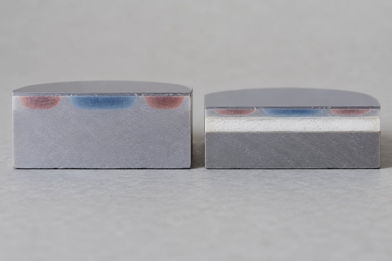
Bulk silicon is a single monolithic crystal in which transistors, wells and isolation structures are all formed together. Silicon-on-insulator (SOI) splits that crystal into three layers: a thin device layer, a buried oxide (BOX) layer, and a supporting handle wafer, so each device is dielectrically isolated from everything beneath it. In this bulk silicon vs SOI comparison, the short version is that bulk silicon is the general-purpose default and SOI pays off when isolation, low leakage or high integration justify extra process and design work.
That is a substrate decision, not a marketing one. It changes your PDK, your design rules, your reliability models and, in some cases, your floorplan. Getting it wrong is expensive to undo, which is why most teams make the call once, carefully, before tape-out.
Table of Contents
- Bulk Silicon vs SOI Comparison at a Glance
- What Is Bulk Silicon?
- Why silicon still dominates as a substrate material
- What Is SOI?
- Bulk Silicon vs SOI: Electrical Performance
- Electrical Behavior: Bulk Silicon vs SOI
- Thermal behavior: why SOI devices self-heat
- Process Complexity, Yield, and Cost
- Design Rules and EDA Support
- Applications and Node Scalability
- Which Should You Choose?
- Frequently Asked Questions
- Is SOI always faster than bulk silicon?
- Does SOI always use less power?
- Which is cheaper to manufacture, SOI or bulk silicon?
- Can you build analog and RF circuits on SOI?
- Is bulk silicon obsolete at advanced nodes?
- How do I decide between bulk silicon and SOI for a new chip?
- Conclusion: Choose Based on the Process Constraint
Bulk Silicon vs SOI Comparison at a Glance
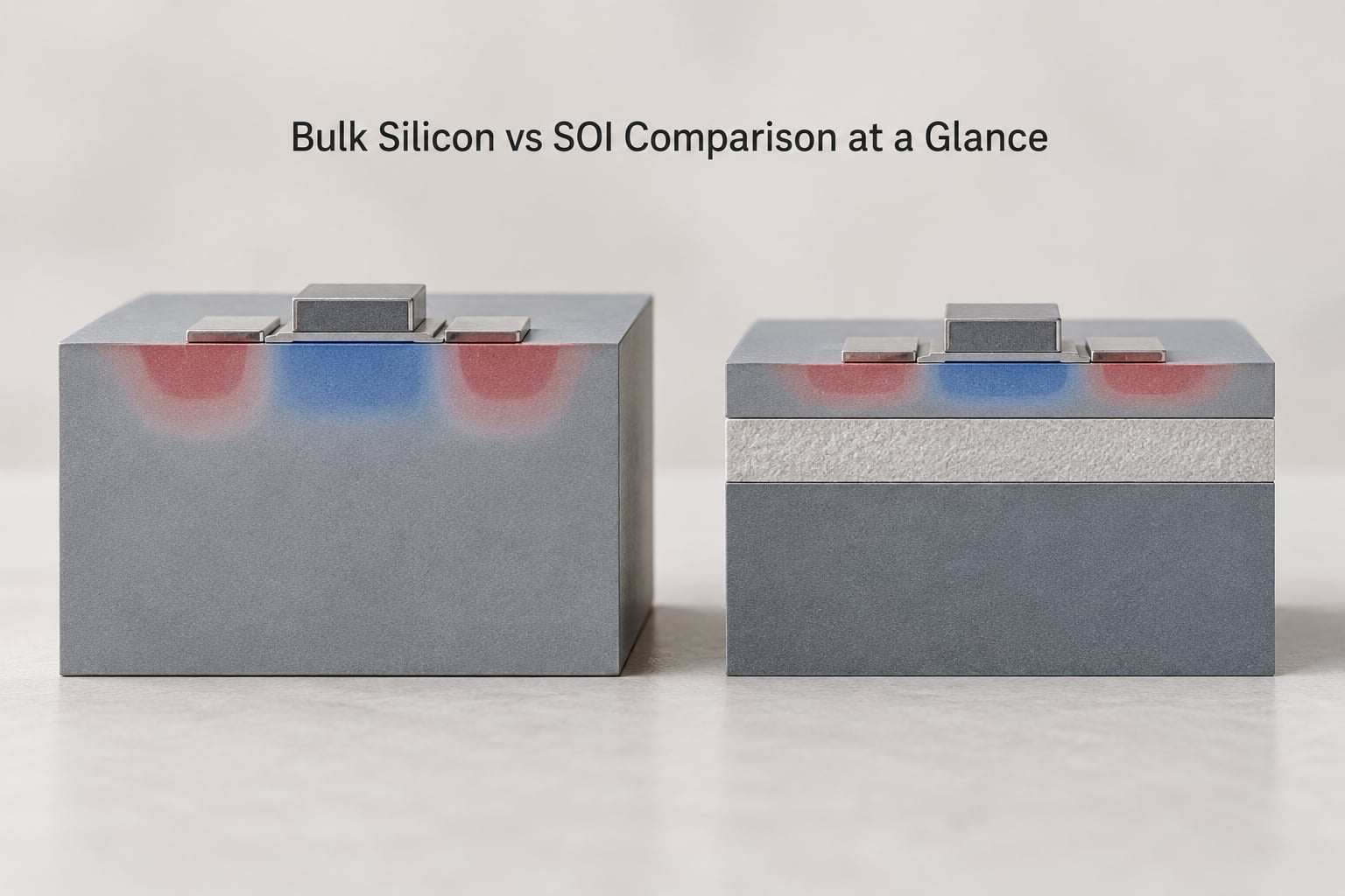
The table below is the whole comparison on one page. Every row is a place where the two technologies genuinely diverge, and the last column tells you which side usually wins in practice.
| Criterion | Bulk Silicon | SOI | Edge |
|---|---|---|---|
| Substrate structure | One monolithic silicon crystal; devices and wells share the same body | Thin device layer over a buried oxide (BOX) layer over a handle wafer | Neither, different architectures |
| Isolation mechanism | Doped wells, trench oxides and reverse-biased junctions | Dielectric isolation by the BOX layer | SOI |
| Parasitic capacitance | Source/drain junction capacitance to wells and substrate | Minimal junction capacitance; BOX capacitance instead | SOI |
| Leakage current | Junction leakage plus subthreshold leakage, both present | Subthreshold leakage only; very low junction leakage | SOI |
| Self-heating | Heat flows into the bulk; silicon conducts heat well | Heat trapped under a thermally resistive BOX layer | Bulk silicon |
| Latch-up | Possible through parasitic pnp/npn structures | Largely eliminated by dielectric isolation | SOI |
| Body biasing | Wells tied to a supply rail; limited threshold tuning | Floating or body-biased film; wide back-bias range on FD-SOI | SOI |
| Body effect / history effect | No floating body; no history dependence | Floating body creates history effect and delay variation | Bulk silicon |
| Short-channel behaviour | Controlled by doping and gate geometry; degrades with scaling | Better electrostatic control from a thin body, lower DIBL | SOI |
| Radiation behaviour | Standard; soft errors from collection in substrate | Reduced charge collection; suited to radiation-sensitive designs | SOI |
| Substrate noise coupling | Noise travels through the shared substrate | BOX blocks substrate noise injection | SOI |
| Wafer cost and supply | Cheaper, abundant, many foundries, every diameter | More expensive; fewer qualified sources; process-limited diameters | Bulk silicon |
| EDA and PDK maturity | Deep libraries and sign-off flows everywhere | Mature at leading foundries, thinner elsewhere | Bulk silicon |
| Best fit | Cost-sensitive, high-voltage, mixed-signal, mature nodes | RF, low-leakage digital, photonics, MEMS, harsh environments | Depends on the application |
What Is Bulk Silicon?
Bulk silicon is the conventional substrate used by most standard integrated circuit processes. The wafer itself is the device body: field-effect transistors are formed at the surface, wells are diffused or implanted into the same crystal, and isolation between neighbouring devices comes from doped regions, reverse-biased junctions and shallow-trench oxides.
That arrangement has three decades of accumulated advantage behind it. Every major foundry runs bulk processes, the design kits cover an enormous range of cells, models and corners, and a wafer is comparatively cheap to buy. For cost-sensitive designs, high-voltage parts, analog and mixed-signal blocks, and anything on a mature node, bulk silicon is simply the path of least resistance.
Why silicon still dominates as a substrate material
Silicon is preferred because it forms a stable, high-quality oxide interface at temperatures a fab can sustain, and that oxide is what makes every CMOS process practical. The oxide passivates the surface, defines gates and isolation regions, and lets a mature thermal budget do most of the work.
Beyond that, silicon is abundant, its oxide and nitride chemistry is well understood, and decades of tooling investment have driven wafer cost down. Supply is not a realistic constraint: silicon is the second most abundant element in the Earth’s crust, so the real question is wafer throughput and qualification, not raw material.
What Is SOI?
An SOI wafer is an engineered substrate with three layers. The top layer is the device layer, a thin film of silicon where the transistors are built. Beneath it sits the buried oxide, commonly called the BOX layer, which does the isolating. Under that is the handle wafer, a thick silicon support that gives the whole structure mechanical strength.
So what is an SOI wafer, functionally? It is a way of giving every transistor its own isolated island of silicon with no junction required. That single change is the origin of nearly every SOI advantage and nearly every SOI problem.
One clarification worth making early: SOI is a substrate and process architecture, not a replacement for CMOS logic. You still build CMOS circuits on it. And it comes in flavours that matter for the decision: partially depleted SOI (PD-SOI) with a device layer of roughly 50-90 nm over a BOX of about 100-200 nm, and fully depleted SOI (FD-SOI) with a device layer of roughly 5-20 nm over a BOX of about 5-50 nm.
Bulk Silicon vs SOI: Electrical Performance
The electrical differences are the reason people choose SOI at all, and they are also the reason it is not a straight upgrade. Everything follows from one fact: in bulk silicon, isolation costs you a junction, and in SOI it does not.
Electrical Behavior: Bulk Silicon vs SOI
Because bulk isolation relies on reverse-biased junctions, every source and drain has capacitance to a well and to the substrate. That capacitance eats drive current, slows edges and adds dynamic power. In SOI those junctions are gone. You pay a BOX capacitance instead, and it is dramatically smaller.
Leakage improves for the same reason. Subthreshold leakage still exists in SOI because it is a transistor physics effect, but junction leakage, which dominates at elevated temperature, largely disappears. In an analog or mixed-signal part running hot, that difference is not academic.
Short-channel behaviour also differs. A thin SOI body gives the gate better electrostatic control of the channel, which suppresses drain-induced barrier lowering and reduces threshold voltage sensitivity to variations in device length. Bulk silicon, by contrast, relies on doping and junction engineering, and that approach degrades as dimensions shrink.
Bulk silicon keeps the edge in one specific area: high-voltage and analog behaviour in mature processes is predictable, well characterised, and heavily qualified in the field. It is rarely a surprise. If your part spends its life at 400 V with a demanding noise specification, that predictability is worth more than a smaller parasitic.
Thermal behavior: why SOI devices self-heat
Silicon conducts heat at roughly 148 W/m·K. The silicon dioxide used for the BOX conducts it at about 1.4 W/m·K, roughly two orders of magnitude worse. A SOI transistor therefore sits on its own thermal island: current flowing through the device heats it, and heat has nowhere efficient to go.
The consequence is a rise in junction temperature, a fall in mobility and threshold voltage, and reduced reliability margins over time. For low-power digital blocks running at modest activity rates, this is usually a manageable trade. For RF front ends and high-current analog stages, it can be the limiting factor, and it is why RF-SOI processes are engineered carefully around thermal paths.
Bulk silicon has no such problem in the same sense. Heat spreads into a large, well-conducting body, so junction temperature tracks ambient much more closely.
Process Complexity, Yield, and Cost
Fabricating SOI wafers requires the silicon device layer to be built or transferred onto the BOX and handle. The main routes are SIMOX, where oxygen is implanted and annealed to form the buried oxide; wafer bonding with UNIBOND or Smart Cut, where a donor layer is transferred onto an oxidised handle; and older methods such as FIPOS and silicon-on-sapphire.
SIMOX is comparatively simple but gives limited control over the thickness of the buried oxide. Wafer bonding gives excellent thickness and uniformity control and is the basis of most production SOI, but it adds bonding, splitting or grinding, and alignment steps. The process is longer, and each extra step is another defect opportunity.
That shows up as lower defect density for the same wafer size and node, which pushes effective die cost up even when the wafer price difference looks modest. It also concentrates supply: a smaller number of suppliers are qualified for leading SOI processes, and some options are limited by available wafer diameter.
The honest summary is that neither substrate is universally cheaper. Cost depends on node, foundry, device type, die size, volume and how much process control the specific design needs. At mature nodes with large analog dies, bulk silicon is usually the economical choice. At leading-edge nodes with demanding leakage budgets, an SOI process may be the only one where the design closes on power at all.
Design Rules and EDA Support
Switching substrates changes the design, not just the mask set. The clearest example is the body. In bulk silicon, the body is tied into wells and a supply rail, so it is stable and predictable. In SOI the body is a thin floating film that accumulates charge through impact ionisation, and the resulting floating body effect creates the history effect: a device’s behaviour depends on what it did a moment earlier.
That history effect shows up as delay variation, asymmetric behaviour between rising and falling transitions, and device mismatch that sign-off has to model rather than ignore. PD-SOI mitigates it because a partially depleted body can supply holes to recombine. FD-SOI largely avoids it because the film is thin enough that the body cannot hold significant charge.
ESD design changes too. Bulk designs lean on well structures, diodes and clamps tied into the substrate. On SOI the same structures behave differently, and clamping has to be reworked around the thin film and its BOX.
Body biasing is where SOI earns its keep. Applying a voltage to the body through the BOX, sometimes called back gating, shifts threshold voltage without changing the circuit. FD-SOI implementations in particular can tune threshold over a useful range, letting you trade dynamic power for leakage after the design is finished.
Standard cells and analog libraries exist for both, but depth differs. Bulk-silicon libraries, particularly at mature nodes, are broader and more mature, with more characterised corners and more proven analog blocks. The lesson is simple: check the target foundry’s actual PDK and design rules rather than assuming the two substrates are interchangeable. They are not.
Applications and Node Scalability
Microprocessors and flagship mobile silicon have been the strongest case for SOI at advanced nodes, because reduced capacitance and leakage matter when you are fighting a power budget at every switching event. Automotive low-power and always-on blocks use FD-SOI for the same reason: the ability to tune threshold voltage in the field.
RF is arguably SOI’s strongest niche. RF switches, power amplifiers and front ends on RF-SOI benefit from high Q, low substrate coupling and strong isolation between adjacent circuits. Silicon photonics and MEMS depend on SOI for the same structural reason: the BOX provides an excellent, well-defined low-index cladding for optical waveguides and a clean mechanical anchor for moving structures.
Bulk silicon holds the other side. Cost-sensitive consumer parts, high-voltage smart power, automotive power domains, most analog and mixed-signal blocks, and much of the display driver market run on mature bulk nodes without any interest in changing. Where volumes are large and the specification is dominated by voltage and noise rather than switching energy, bulk silicon is the settled answer.
This bulk silicon vs SOI comparison has no universal winner by node. What scales is the ratio of dynamic power to leakage power. When dynamic power dominates, reduced capacitance pushes design toward SOI. When leakage dominates and voltage scaling has stalled, body biasing on FD-SOI becomes attractive. That is why advanced logic and mature analog have diverged rather than converging on one substrate.
Which Should You Choose?
Choose bulk silicon when you are on a mature node, need high voltage, want the widest choice of analog and power IP, or simply cannot justify qualifying a process you are not already using. Choose SOI when leakage reduction, strong isolation, reduced capacitance, or access to a foundry-qualified high-performance process is the actual constraint.
A short checklist helps. Confirm the target node and whether an SOI process exists there at all. Confirm your voltage range, because high-voltage parts usually push toward bulk. Set the power target and decide whether leakage or switching energy dominates. List the IP you actually need, including analog blocks and memories, and confirm they exist for the chosen process. Then look at wafer volume and supply, because a single qualified source is a schedule risk for a high-volume part.
If the answers point both ways, prototype the critical block on both processes. Thermal margin and leakage behaviour are much easier to measure on silicon than to argue about in a spreadsheet.
Frequently Asked Questions
Is SOI always faster than bulk silicon?
No. SOI reduces parasitic capacitance and improves electrostatic control of the channel, which usually helps switching speed at the same node. But speed also depends on gate length, mobility, interconnect and voltage, and a bulk process on a smaller node can still be faster. This bulk silicon vs SOI comparison treats speed as one factor among several, not a verdict on its own.
Does SOI always use less power?
Not always. SOI cuts dynamic power by lowering junction capacitance and cuts leakage by removing most junction leakage. However, self-heating raises junction temperature, which raises leakage and can erode the advantage. For low-activity-rate or low-leakage designs the gain is clear; for high-current RF or analog stages the thermal penalty can eat much of it.
Which is cheaper to manufacture, SOI or bulk silicon?
Bulk silicon is generally cheaper. SOI needs extra steps to form or transfer the device layer onto the buried oxide and handle wafer, which lowers defect density at a given die size and concentrates supply among fewer qualified suppliers. At mature nodes with large analog dies the gap is decisive. At leading nodes an SOI process may still be the only route that meets the power target.
Can you build analog and RF circuits on SOI?
Yes. RF-SOI is a mature commercial reality for switches, power amplifiers and front ends, and analog and mixed-signal blocks appear on SOI processes in volume products. The differences to plan for are self-heating in high-current stages and floating body behaviour, which need attention in device choices and layout. Confirm the specific blocks you need exist in the target PDK.
Is bulk silicon obsolete at advanced nodes?
No. Bulk silicon remains the default for mature nodes and dominates high-voltage, power and analog designs. At the most advanced logic nodes, multi-gate transistor architectures rather than the substrate choice dominate the discussion, and both bulk and SOI variants exist in some processes. The substrate decision is driven by power and isolation needs, not by a simple rule about how small the node is.
How do I decide between bulk silicon and SOI for a new chip?
Start from the constraint, not the preference. Write down the node, the voltage range, the power budget, the required IP and the expected wafer volume. Then ask which foundry process meets all five with a qualified PDK. That usually makes the choice for you. If two processes still fit, compare the leakage-critical and thermal-critical blocks rather than guessing at a general winner.
Conclusion: Choose Based on the Process Constraint
Bulk silicon wins on cost, thermal conductivity, ecosystem depth and predictability. SOI wins on isolation, parasitic capacitance, leakage, latch-up immunity and the flexibility that body biasing and thin bodies give you. Every real design team that picked the “wrong” one did so by choosing a substrate before writing down the constraint.
Start with the process, not the technology: identify the target node, voltage range, power budget, required IP and foundry process. Then pick the substrate the qualified PDK supports. In this bulk silicon vs SOI comparison, that sequence decides the question far more reliably than any general rule about which technology is better.