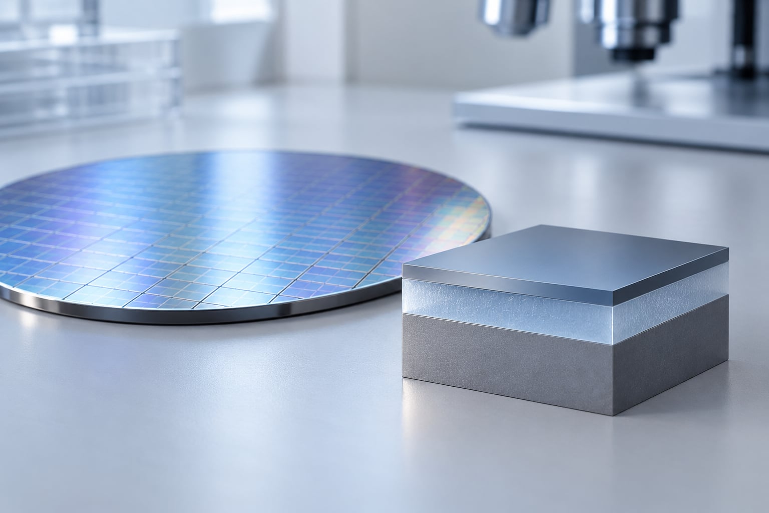
An SOI wafer is a silicon substrate built in three layers: a thin single-crystal silicon device layer where transistors are fabricated, an insulating buried oxide (BOX) layer usually made of silicon dioxide, and a thick silicon handle wafer that gives the whole stack mechanical strength.
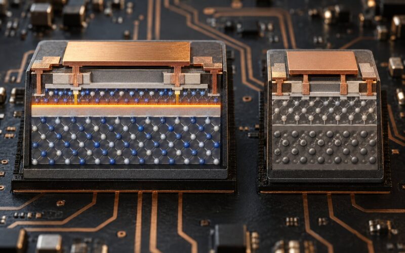
That middle oxide is the whole point. On bulk silicon every transistor sits on a shared, electrically live substrate. On SOI each device floats on its own insulator, which cuts parasitic capacitance, removes substrate coupling and CMOS latch-up, and lets circuits run at lower voltage. Designers reach for an SOI wafer when power, isolation, RF linearity or optical confinement matters more than getting the cheapest possible wafer.
Key takeaways:
- The three-layer stack is device layer, buried oxide (BOX), handle wafer.
- BOX isolates every device electrically and thermally from the bulk.
- Lower parasitic capacitance means lower dynamic power and faster switching.
- The handle wafer exists for handling, support and backside processing, not for circuitry.
- SOI costs more per wafer and runs hotter, so it is a targeted choice rather than a universal upgrade.
Table of Contents
- What SOI Wafers Are and How They Work
- How SOI Wafers Differ from Conventional Silicon Wafers
- Why SOI Wafers Reduce Power and Improve Performance
- When Are SOI Wafers Used in Practice?
- RF-SOI and mixed-signal
- Fully depleted SOI logic
- Silicon photonics
- MEMS sensors and actuators
- Power management and mixed-signal
- Radiation-tolerant and emerging work
- What Are the Main Types of SOI Technology?
- What Are the Limitations of SOI Wafers?
- How Designers Choose Between SOI and Bulk Silicon
- Frequently Asked Questions
- What is an SOI wafer?
- How is an SOI wafer made?
- Why does an SOI wafer still have a silicon handle wafer underneath?
- What are the disadvantages of SOI wafers?
- When should I choose SOI instead of bulk silicon?
- Do SOI wafers cost more than bulk silicon wafers?
- Conclusion
What SOI Wafers Are and How They Work
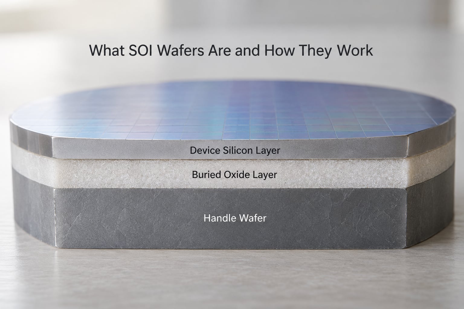
Read an SOI wafer from the top down and it is simple to describe, which is why the concept slips past people who have only worked with bulk silicon.
- Device layer. The thin top layer of single-crystal silicon where the active devices are actually built. Suppliers quote this as a thickness with a tolerance, and the figure you pick depends entirely on what you are making. Supplier specification sheets commonly range from well under a micron for fully depleted logic to tens or hundreds of microns for photonics, power and MEMS work.
- Buried oxide (BOX) layer. A thermal silicon dioxide layer, typically somewhere between a few hundred nanometres and a few micrometres depending on the application. It is an electrical insulator, so it blocks both DC current and capacitive coupling to anything below it.
- Handle wafer. The thick silicon base. It gives the wafer rigidity for handling, supports backside processing such as thinning and heat sinking, and gives the BOX something to sit on.
That last point comes up constantly in engineering forums. If the goal is insulation, why keep silicon underneath at all? Because a 100 nanometre film cannot be diced, shipped, aligned in a lithography tool or ground from the back without shattering. The handle wafer is a mechanical chassis, not an electrical participant.
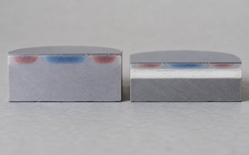
Electrically, the change is straightforward. In bulk CMOS each transistor is formed in a continuous silicon body and separated from its neighbours by doped well regions and reverse-biased junctions, which leak some current and add capacitance. On SOI the BOX cuts each device off from everything beside and beneath it, so isolation is structural rather than engineered through doping.
How SOI Wafers Differ from Conventional Silicon Wafers
Bulk silicon is one continuous crystal with devices carved into its surface. SOI replaces that continuous body with a thin film sitting on an insulator. The table below covers what actually changes for a designer.
| Property | SOI wafer | Bulk silicon wafer |
|---|---|---|
| Structure | Device layer, buried oxide, handle wafer | Single continuous silicon crystal |
| Device isolation | Buried oxide barrier, near total | Doped wells and reverse-biased junctions |
| Substrate capacitance | Very low, oxide barrier | Higher, junction and body capacitance |
| Substrate coupling and noise | Largely suppressed | Present, worsens with frequency |
| CMOS latch-up | Structurally prevented | Possible, needs guarding |
| Typical operating voltage | Lower voltage operation is practical | Higher supply for comparable performance |
| Switching speed | Higher at a given node | Lower at the same node |
| Heat path to handle wafer | Interrupted by oxide | Direct through silicon |
| Body effect handling | Floating body, needs design care | Body tied to a well, well behaved |
| Substrate cost | Higher, quote based | Lower, mature high volume supply |
| Typical uses | RF front ends, FD-SOI logic, photonics, MEMS, power | Mainstream CPUs, GPUs, DRAM, general logic |
The practical consequence is that an SOI design can hit a target on a less advanced, cheaper process node than a bulk design would need, because the isolation does work that a bulk design pays for in bigger transistors and higher voltage.
Why SOI Wafers Reduce Power and Improve Performance
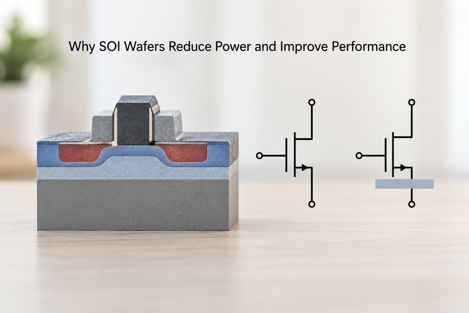
Dynamic power in CMOS scales with capacitance and with the square of supply voltage. Cut capacitance and you can often cut voltage too, and voltage has a squared effect on dynamic power. That is the main lever SOI pulls.
Reduced parasitic capacitance is the first benefit, because the oxide removes the large source-drain and body capacitances to substrate that dominate a bulk transistor. Less capacitance to charge means shorter switching time and less energy per transition, so a circuit hits its clock target at a lower supply voltage.
Second is isolation. Without shared wells, neighbouring devices stop interfering through the substrate, so analog blocks sit next to digital ones with far less crosstalk, and RF front ends see less injected noise on sensitive paths.
Third is drive current. A fully depleted SOI device has better control of the channel and can deliver more current at a given voltage, which raises the ceiling on single-thread performance at nodes where bulk silicon is struggling.
There are limits worth naming. Short-channel effects, subthreshold slope and variability do not vanish just because the body is floating, and at the smallest nodes the mainstream answer is FinFET or gate-all-around devices built on bulk or epitaxial substrates instead. SOI gains come from the isolation, not from being newer.
When Are SOI Wafers Used in Practice?
Applications split along the lines of what the oxide layer gives you electrically, optically or thermally.
RF-SOI and mixed-signal
RF switches, antenna tuners and front-end modules rely on high isolation between a high-voltage signal path and the low-voltage control logic beside it. SOI delivers that isolation directly in the substrate, which lets RF-SOI integrate what previously needed separate components. Low substrate noise also helps the linearity that receiver chains need.
Fully depleted SOI logic
FD-SOI uses a thin device layer, typically on the order of a few nanometres to a couple of dozen nanometres depending on the node, so the channel is fully depleted of charge carriers when the transistor is off. That enables back-biasing: engineers raise or lower the body voltage to trade leakage for speed without changing the design. This is the branch of SOI behind the 22FDX platform at GlobalFoundries and the 28FD-SOI process at STMicroelectronics, both commercial FD-SOI offerings still shipping as of 2026.
Silicon photonics
Silicon photonics is the largest and most mature photonics use of SOI. A buried oxide with a high refractive-index contrast against the device silicon confines light in the layer above, allowing waveguides, modulators, photodetectors and ring resonators to be patterned with tight bends. Without the oxide, light spreads into the substrate and the waveguide losses climb. The same high-index structure also makes high-Q resonant filters practical.
MEMS sensors and actuators
Accelerometers, gyroscopes, pressure sensors and micro-mirror devices use the buried oxide as a release surface. A structural layer is patterned above it and the oxide underneath is etched away in selected areas, leaving suspended structures that move. The oxide also acts as an etch stop, which keeps release etch selectivity high.
Power management and mixed-signal
Power management ICs integrate switching regulators, analog blocks and control logic that would disturb each other badly on a shared conductive substrate. Isolation cuts that coupling. Higher-voltage capable device layers and thicker buried oxide are common in this application, and thin-handling is not the constraint.
Radiation-tolerant and emerging work
SOI is used in aerospace and defence electronics because the thin device layer reduces the charge collected by a particle strike, which helps with single-event effects and total ionizing dose behaviour. Researchers also use engineered SOI substrates for cryogenic control electronics, quantum device work and neuromorphic circuits, where custom layer thicknesses matter more than volume.
What Are the Main Types of SOI Technology?
The name describes a family of substrates, and the insulating layer is what varies.
- Silicon-on-silicon. The dominant commercial form, with a silicon dioxide buried oxide on a silicon handle wafer. Smart Cut layer transfer, SIMOX and bonded processes all produce this structure.
- Silicon-on-sapphire (SOS). Sapphire replaces the buried oxide. It offers good isolation and RF behaviour, and it was used before silicon-on-silicon was practical, but sapphire is expensive, brittle and thermally conductive in a way that constrains power handling.
- Silicon-on-glass (SiOG). A glass or glass-like buried layer, used mainly for optoelectronics, sensors and waveguide purposes rather than high-performance logic.
- Silicon-on-diamond. Diamond sits under the device layer to spread heat, used where thermal management dominates the design problem.
- SiGeOI. A silicon-germanium device layer on oxide, used for higher mobility in some analog and RF work.
One thing to keep straight: SOI is a wafer platform, while FinFET and fully depleted devices are transistor architectures. They are not the same axis, and some FD-SOI platforms use planar transistors precisely because isolation already handles part of what a fin provides.
What Are the Limitations of SOI Wafers?
SOI is not a drop-in upgrade from bulk silicon, and treating it as one causes expensive late surprises.
Self-heating is the main one. Silicon dioxide conducts heat roughly two orders of magnitude worse than silicon, so the oxide insulates the hot spots instead of carrying heat away. Local temperature rises drive down carrier mobility and accelerate ageing. Design responses include shorter low-voltage operating points, staggered layouts, more spacing around hot devices and backside heat sinking, but the constraint never disappears.
The floating body effect is the second. With the body electrically isolated, charge can accumulate in the device layer and float the body potential, which affects threshold voltage, causes history effects and can degrade output current. Bulk silicon ties the body to a well, so this does not happen the same way. Body ties, body diodes and careful body biasing manage it, and it is a genuine design cost.
Cost and supply are real constraints. Substrate pricing is quote-based and moves with diameter, device layer and buried oxide thickness, fabrication method, grade and volume. Unusual specification combinations can carry minimum quantities, which is exactly the friction university and MEMS labs run into. Thin SOI wafers are also more fragile to handle and ship than bulk silicon at small diameters.
Process integration takes work. Existing bulk-qualified PDK flows, analog libraries and test methods do not transfer directly. Porting a design is a project, not a swap, and that effort belongs in the comparison.
How Designers Choose Between SOI and Bulk Silicon
Start from the constraint that is hardest to relax, not from a feature list.
Choose SOI when the design needs electrical isolation between neighbouring blocks, when the supply voltage target is low and dynamic power dominates, when RF linearity or switch isolation sets the architecture, when light has to be confined on-chip, when a MEMS structure needs a defined release layer, or when substrate noise and latch-up are already limiting the bulk design.
Stay with bulk silicon when the design is cost-led at high volume, when heat has to leave the device through the substrate, when the logic sits at a node where bulk FinFET or gate-all-around is the better-supported option, or when an existing mature process, PDK and analog library already meet the requirements.
The device layer thickness is where most of these decisions land. The ranges below are typical supplier offerings, and the value you need is set by the physics of your device rather than by preference.
| Device layer thickness (typical) | Primary use | Reason it matters |
|---|---|---|
| Very thin, a few nanometres to tens of nanometres | Fully depleted SOI logic | Channel fully depletes for back-biasing and leakage control |
| Sub-micron to a few micrometres | Advanced MEMS, cavity SOI | Moves on the order of microns and cavity structures stay defined |
| Mid-range, several micrometres | RF-SOI, mixed-signal | Device room plus controlled high-voltage behaviour |
| Thick, tens of microns and above | Silicon photonics, power devices, detectors | Waveguide mode confinement and thermal spreading |
A few questions settle it faster than a feature matrix: what is the target supply voltage, what is the power ceiling in milliwatts, does the design need on-chip light or suspended mechanical structures, is there RF content, how much heat must leave the die, and does a foundry or substrate supplier actually offer the specification you need in your volume?
If the answer to that last question is no, the design has a sourcing problem regardless of how good the physics is. Confirm availability first.
Frequently Asked Questions
What is an SOI wafer?
An SOI wafer, or silicon-on-insulator wafer, is a three-layer silicon substrate: a thin single-crystal device layer where transistors are built, a buried oxide (BOX) layer that acts as an electrical insulator, and a thick silicon handle wafer that provides mechanical support. The oxide isolates each device from the bulk and from its neighbours.
How is an SOI wafer made?
The main routes are SIMOX, where oxygen is implanted into silicon and annealed into a buried oxide; wafer bonding and etch-back, where two wafers are bonded and one ground away; Smart Cut layer transfer, where a hydrogen-implanted layer is transferred onto the target wafer; and ELTRAN, a variation on the bonded approach. Each method reaches different thickness control and uniformity.
Why does an SOI wafer still have a silicon handle wafer underneath?
The handle wafer is mechanical, not electrical. It gives a structure whose active film is far too thin to dice, ship, align in a lithography tool or grind from the back on its own. It also carries backside processing such as thinning and heat sinking, and it grounds the substrate electrically.
What are the disadvantages of SOI wafers?
Silicon dioxide conducts heat far worse than silicon, so SOI devices self-heat, which lowers mobility and shortens life. The isolated body floats, which causes threshold shifts and history effects that bulk silicon does not have. Substrates also cost more, porting an existing bulk design takes real effort, and uncommon specifications can carry minimum order quantities.
When should I choose SOI instead of bulk silicon?
Choose SOI when isolation between blocks, low supply voltage, low dynamic power, RF switch isolation, on-chip optical confinement, or a defined MEMS release layer is a design requirement rather than a nicety. Stay with bulk when cost at high volume, heat removal through the substrate, or an already mature process and PDK dominate the decision.
Do SOI wafers cost more than bulk silicon wafers?
Yes, per wafer. Substrate pricing is quote-based rather than published and moves with diameter, device layer and buried oxide thickness, fabrication method, grade and order volume. Compare total system cost instead: lower operating voltage, smaller die area and reduced cooling can offset a higher substrate cost, and only a supplier quote for your exact specification will settle it.
Conclusion
An SOI wafer is silicon on an insulator, and every benefit and every headache traces back to that one buried oxide layer.
Start with your hardest constraint: if it is isolation, low voltage, RF behaviour, light confinement or a MEMS release surface, an SOI wafer is likely the right substrate and the device layer thickness is your first specification decision. If it is cost per die or heat removal through the substrate, bulk silicon is probably still the better answer. Confirm that a supplier offers your exact stack in your volume before designing around it, and then ask for a quote rather than assuming a number.