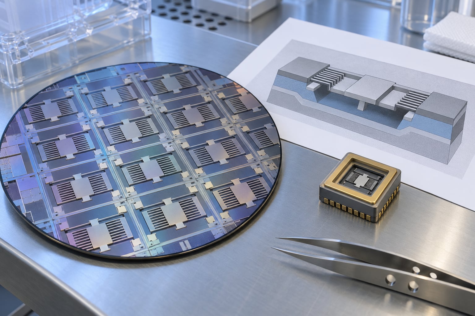
What a MEMS device is and how it is made comes down to one idea: a MEMS device puts tiny moving mechanical parts and sensing electronics on the same silicon wafer. The mechanical piece reacts to acceleration, pressure, sound or rotation, and the electronics turn that reaction into a signal you can read. Because they are batch fabricated, one wafer yields thousands of them at once.
The term itself is short for microelectromechanical system. It is not a new invention layered onto chipmaking, either. MEMS rides on the same photolithography, deposition and etching tools that make ordinary transistors, then adds a handful of steps to carve out structures that can move.
Below is the working picture: what the parts are, what makes them different from a normal chip, the full wafer flow, and what happens after the die leaves the fab. If you want the one-line version first, skip to the fabrication steps.
Table of Contents
- What Is a MEMS Device?
- How Does a MEMS Device Work?
- Worked example: a capacitive accelerometer
- How Is a MEMS Device Different From a Conventional IC?
- What Are the Main Parts of a MEMS Device?
- How Is a MEMS Device Made?
- What a MEMS Device Is Made Of
- How the Wafer Process Creates Tiny Moving Structures
- How Are MEMS Devices Packaged and Tested?
- Frequently Asked Questions
- What is the difference between MEMS and NEMS?
- Are MEMS devices semiconductor chips?
- Do MEMS devices have moving parts?
- Is a clean room required to make MEMS devices?
- How small can a MEMS device be?
- What is the difference between monolithic and hybrid MEMS?
- Conclusion
What Is a MEMS Device?
A MEMS device is a microscopic electromechanical system that combines a moving or deforming mechanical structure with electronics, built on a single silicon substrate at the micrometre scale.
You have probably used several today without noticing. Phone motion sensing, the step counter in a watch, the microphone in an earbud, the pressure sensor in a car tyre, and the airbag trigger in a front seat are all MEMS parts. So are the tiny mirrors that steer a laser beam in a projector and the switches that route radio signals on a communications board.
Scale is the part people remember. A human hair is roughly 70 micrometres across, and MEMS gaps between a moving electrode and a fixed one can be a couple of micrometres or less. Thousands of these structures fit across one die, and a single 200 mm wafer holds hundreds of thousands of them.
Two families matter. Sensors read something from the world and report it as an electrical value: accelerometers, gyroscopes, pressure sensors, magnetometers, microphones, inkjet printheads. Actuators take an electrical value and produce motion, light or flow: micro-mirrors, micro-pumps, RF MEMS switches, micro-heaters. Plenty of devices do both.
How Does a MEMS Device Work?
A MEMS device works by converting physical movement into something electrical, usually a change in capacitance, resistance or frequency.
Every design has four functional pieces. The mechanical structure is the part that moves: a suspended proof mass, a flexible diaphragm, a resonant beam. The sensing element translates that motion into an electrical quantity, most often a change in the capacitance between two electrodes. The electronics amplify, filter and convert the signal, and they may also run a control loop. On an actuator, a drive element pushes the structure instead: electrodes that pull a comb drive sideways, or a resistive heater that bends a bimetal beam.
Worked example: a capacitive accelerometer
Imagine a small plate suspended inside the die on four thin springs, with fixed electrodes above and below it. When the package accelerates, inertia makes the plate lag behind, and the springs displace it by a fraction of a micrometre.
That shift changes the gaps to the fixed electrodes asymmetrically. The capacitance to one side rises while the capacitance to the other falls. The electronics charge and discharge the two capacitors alternately and measure the current difference, which is proportional to displacement and therefore to acceleration.
Two accelerometers on the same die, mounted at a right angle to each other, give two axes. Add a third axis and a gyroscope, and you have the inertial measurement unit in a watch or a phone. No gyroscope is the same kind of device though: it senses Coriolis force, where a vibrating proof mass experiences a deflection perpendicular to its drive direction when the package rotates.
How Is a MEMS Device Different From a Conventional IC?
A MEMS device differs from a conventional integrated circuit in one fundamental way: it contains parts that move, and a transistor does not.
That single difference cascades into the process, the package and the test plan. Neither technology is universally better. An IC wins on density and switching speed, and MEMS wins on sensitivity, power draw and cost per unit of motion or pressure.
| Aspect | MEMS device | Conventional IC |
|---|---|---|
| Physical behaviour | Has moving or deforming parts that respond to a physical quantity | Static: transistors switch and route signals |
| Typical feature role | Springs, proof masses, membranes, comb fingers, resonators | Transistors, interconnects, capacitors |
| Common materials | Single-crystal silicon, polysilicon, silicon nitride, oxide, metals, sometimes polymers | Silicon, silicon dioxide, copper, low-k dielectrics |
| Process signature | Adds bulk micromachining, DRIE, sacrificial films and a release step | Adds nothing mechanical; layers are deposited and patterned only |
| Release step | Sacrificial layer etched away so structures free themselves | None |
| Packaging | Needs a cavity, a cover and often a controlled reference pressure | Standard moulded or cavity packages |
| Main failure concerns | Stiction, fracture, package stress shifting sensitivity, sealing leaks | Electromigration, oxide breakdown, ESD |
| Typical test | Electrical plus motion, vibration, pressure and thermal cycling | Electrical, often at wafer probe and final test |
What Are the Main Parts of a MEMS Device?
Different architectures use different names, but almost every MEMS device is assembled from the same small set of parts.
- Substrate. The silicon wafer or SOI handle wafer everything is built on and anchored to.
- Proof mass. The heavy central element that lags behind when the package accelerates or rotates. Sometimes it is a perforated plate, sometimes a solid block of doped silicon.
- Suspension springs. Thin beams, usually polysilicon or single-crystal silicon, that let the mass move and return it to rest. Their stiffness sets the resonant frequency and sensitivity.
- Membranes, cantilevers and resonators. Flexible plates and beams used for pressure sensing, mass sensing and frequency-shift detection.
- Comb drives. Interlocking finger electrodes that convert an electrostatic field into sideways motion, used in actuators, gyroscopes and some capacitive sensors.
- Sensing and drive electrodes. Fixed electrodes above, below or beside the moving structure, forming the capacitors that sensing reads and actuators drive.
- Interconnects and bond pads. Metal routing that carries bias, excitation and signal out of the die.
- Control electronics. Charge amplifiers, ADCs, oscillators and digital correction logic.
- Package. The lid, cavity and seal that protect the moving structure from contamination, moisture and shock.
Where the electronics live is a real design choice. In a classic hybrid build, the mechanical sensor die is bonded to a separate CMOS ASIC in the same package, and the ASIC handles everything electrical. In a monolithic CMOS-MEMS build, the mechanical layer is added on top of a standard CMOS wafer so the amplifier sits within microns of the sensor. That shortens the signal path but constrains the process and the mechanical design.
How Is a MEMS Device Made?
A MEMS device is made through a controlled sequence of deposition, lithography, etching, structural release, packaging and testing. Here is the full flow from specification to a tested part.
- Specify the device and design the process. Engineers choose the sensing principle, then model the mechanical structure for stress, fatigue life and mode frequencies before drawing a single layout. The process module is designed alongside the device, since a structure that is theoretically correct can be unmanufacturable.
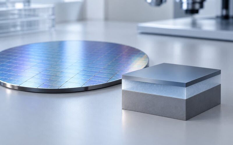
- Prepare the wafer. A prime silicon wafer or SOI wafer enters the fab, cleaned, inspected and sometimes thinned from the back to reduce mass and stress. Handle wafers and carrier wafers may be bonded on for later wafer-level steps.
- Deposit the films. Insulators, the sacrificial layer and the structural layer are laid down by thermal oxidation, low-pressure or plasma-enhanced chemical vapour deposition, sputtering or evaporation. Layer stress is tuned here, because a tensile structural film can curl a released beam.
- Pattern the structural layer. Photoresist is spun on, exposed through a mask and developed. The pattern is then transferred into the film by a dry or wet etch, defining anchors, springs, masses and electrode plates.
- Carve deep structures where bulk micromachining is used. Deep reactive ion etching, usually the Bosch process, cuts trenches with near-vertical walls tens of micrometres deep, straight down into the silicon substrate.
- Add the electrical layer. Contacts, vias and metal interconnect are deposited and patterned, then passivation is opened over the bond pads. If electronics are integrated, the CMOS steps happen here or in a dedicated module.
- Release the moving parts. The sacrificial layer is etched away in a vapour-phase step, typically using HF vapour or a dry release, so the springs and masses become mechanically free. The wafer is dried by critical point drying so surface tension during evaporation does not pull the structures down onto the substrate.
- Dice and package. The wafer is thinned if needed, diced into dies, and each die is attached in a cavity package with a cover. Some flows instead seal at wafer level before dicing, which protects the structures from dicing debris and coolant.
- Calibrate and test. Each part is trimmed, its offset and sensitivity are measured and stored in on-chip memory or fuses, then it goes through electrical, motion, vibration and thermal tests before shipping.
What a MEMS Device Is Made Of
A MEMS device is made of deposited films and patterned layers, and each material earns its place for a specific reason.
Single-crystal silicon forms masses and beams because it is stiff, light and stress-tunable through doping. Polysilicon is easier to deposit and pattern in complex shapes, so it is common for springs and electrodes. Silicon dioxide serves as an insulator and as a sacrificial layer when it can be removed later, and silicon nitride works where chemical resistance or a low-stress film matters. Aluminium, copper and other metals make the electrodes and routing, though metal brings its own stress problem.
Photoresist is the temporary mask material, applied and stripped many times. Sacrificial layers are the films chosen to vanish during release without attacking the structure. SOI wafers give a buried oxide that both defines a device layer and acts as a natural etch stop. Polymers appear in flexible MEMS, where a plastic substrate is needed for curved surfaces and low cost rather than stiffness.
The choice is driven by the sensing principle and the process in use. A capacitive device cares about insulation and gap control; a resonant device cares about film stress; a magnetic sensor cares about keeping stray fields low.
How the Wafer Process Creates Tiny Moving Structures
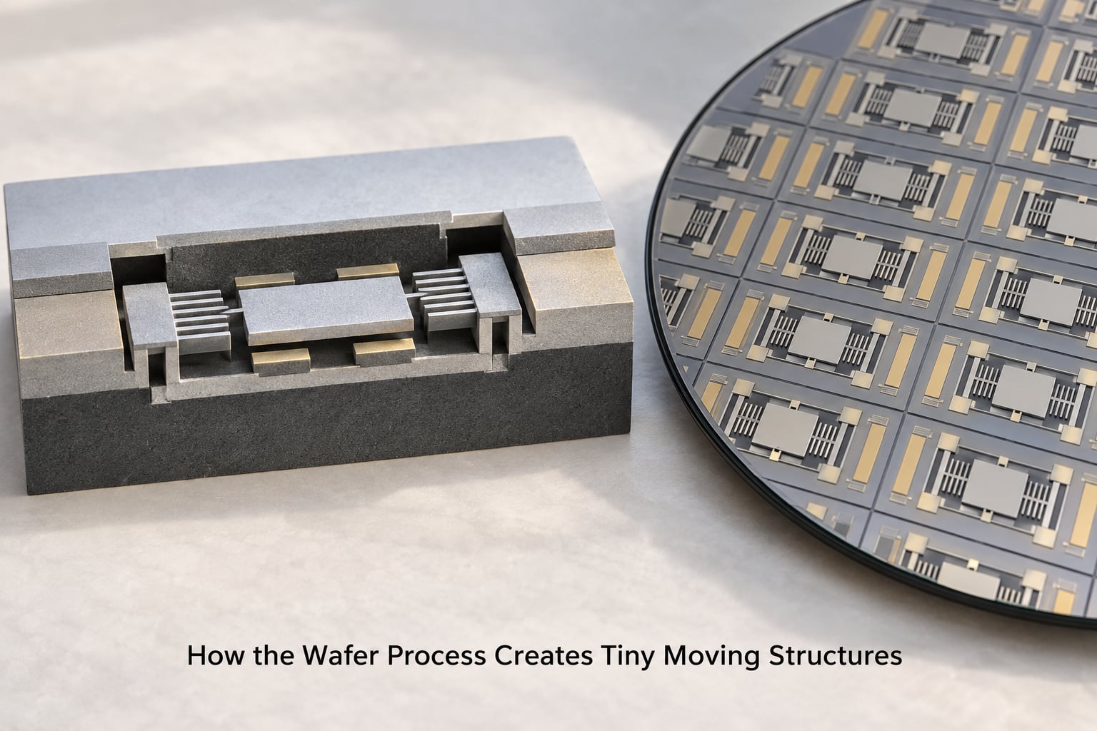
Moving structures come from two main process families. Surface micromachining builds them out of deposited films sitting on top of the substrate. Bulk micromachining removes the substrate itself to define thick, rigid masses and deep cavities. LIGA, a name that comes from the German lithography, electroforming, injection moulding and casting process, is used less often and takes a different route through thick photoresists and electroplated metal.
| Technique | What it does | Typical depth | Common uses | Trade-off |
|---|---|---|---|---|
| Surface micromachining | Deposits and patterns films above the wafer surface, then removes a sacrificial film to free them | A few micrometres | Accelerometers, gyroscopes, RF switches, microphones | Planar and repeatable, but moving mass is limited by film thickness |
| Bulk micromachining | Etches into the silicon substrate to form thick masses and cavities | Tens to hundreds of micrometres | Pressure sensors, gyroscopes, resonators, optical switches | Heavier and more sensitive, but less planar and harder to combine with CMOS |
| LIGA | Uses thick resist lithography and electroforming to build metal structures | Can reach hundreds of micrometres | Microfluidics, connectors, RF components | Very tall structures, but limited wafer-scale economics |
Deep reactive ion etching is the workhorse that made modern three-dimensional MEMS practical. A plasma generated in a vacuum chamber uses a fluorinated chemistry to etch silicon in a repeating cycle: a polymer passivation coats the sidewalls, the bottom is bombarded by ions that clear the polymer and etch downward, then the cycle repeats. The result is a trench that is deep and almost perfectly vertical, which is what allows structures to be carved in every direction instead of only along the wafer plane.
Release is the step beginners should spend the most time on. Until the sacrificial layer is gone, the structures are still anchored to the substrate and look like plain topography. Removing it frees them, and that is when stiction appears: capillary forces during drying pull the released beam toward the surface, and surface tension plus stiction holds it there permanently. Critical point drying avoids the liquid-to-gas transition that creates the force in the first place, and vapour-phase release reduces how much liquid is ever present. Still, release is a top source of yield loss, and contamination left on the wafer makes it worse.
How Are MEMS Devices Packaged and Tested?
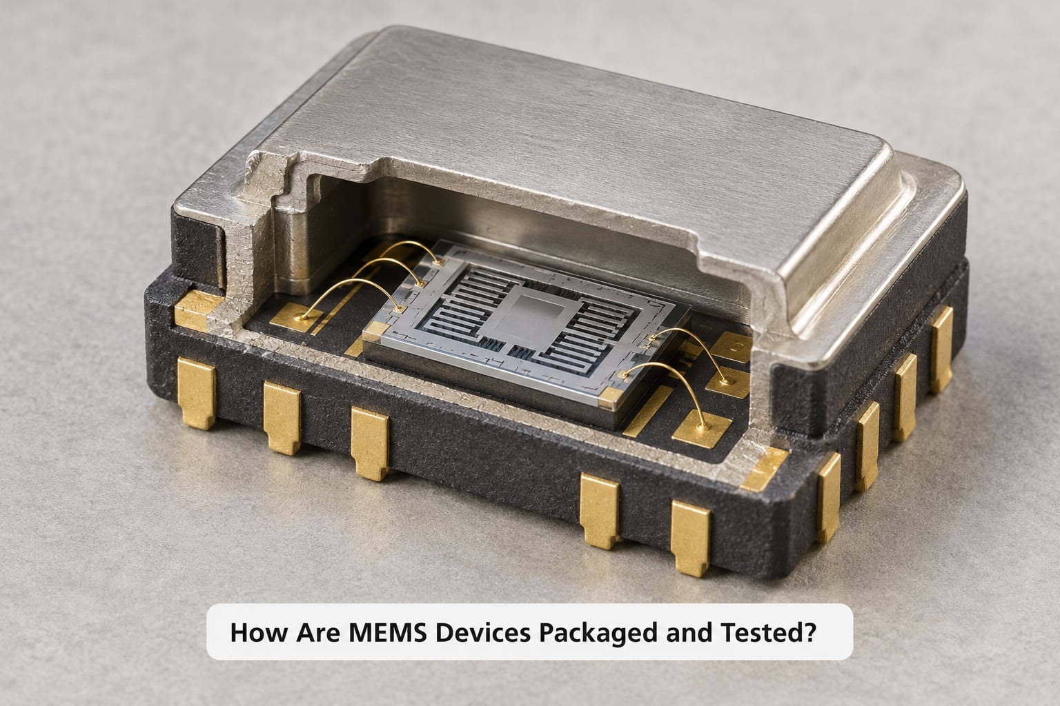
MEMS devices are packaged and tested in ways that protect the moving structure, because a single particle, droplet or shock can ruin a part that passed every electrical check.
The package does three jobs. The cover keeps dust, moisture and handling energy off the mechanical layer. The cavity between die and cover gives the structure room to move and, for absolute pressure sensors, holds a controlled reference vacuum so the die can measure absolute rather than differential pressure. The seal has to stay hermetic for years, and the die attachment has to sit outside the area where the structure moves.
Wafer-level packaging closes the cavity on the wafer before dicing. A cap wafer is bonded to the device wafer, often using a glass or metal seal ring that protects the active area, and electrical vias carry signals through to the outside. Doing it at wafer level means each die is protected from saw coolant and grinding debris, which are a common source of damage. Die-level packaging puts a separate machined or moulded lid over each individual die and is still used where a specific cavity depth or pressure level is required.
Package stress is the quiet problem. Solder, die attach materials and the lid all expand at different rates, and that mismatch puts constant force on the springs and membranes. A pressure sensor can shift by a noticeable fraction of its range just from the package, which is why calibration happens after assembly, not at wafer probe.
Testing runs in layers. Wafer probe checks each die electrically on the uncut wafer and can burn in trim values while it is still cheap to discard. Optical inspection catches stuck structures, missing springs and particles before they are ever packaged. Final test puts the part on a shaker table or a rotary stage to verify axis response, cross-axis sensitivity and frequency response. Barometric parts are checked against a reference chamber, microphones against a calibrated acoustic source, and every package goes through thermal cycling and humidity exposure to prove the seal holds.
Frequently Asked Questions
What is the difference between MEMS and NEMS?
MEMS and NEMS are the same idea at different scales. MEMS works in the micrometre range, with features from roughly 1 to 500 micrometres. NEMS pushes below 100 nanometres. Because NEMS masses are tiny, they respond faster and survive shock better, but they are far harder to release, package and handle without contamination.
Are MEMS devices semiconductor chips?
They are made with semiconductor processes, but they are not integrated circuits. A MEMS device contains moving or deforming parts that a chip does not have, and it usually works alongside a separate CMOS chip that conditions the signal. Some designs use a CMOS-MEMS process to build the electronics and the mechanical layer on a single die.
Do MEMS devices have moving parts?
Yes. Diaphragms, cantilevers, proof masses on springs, comb drives and micro-mirrors all move during operation, usually by fractions of a micrometre up to a few micrometres. That movement is the point of the device. It is what turns acceleration, pressure, sound or rotation into a change an electronic circuit can measure.
Is a clean room required to make MEMS devices?
Yes, a controlled clean room, though the level depends on the process. Deposition, lithography and etching need particulate and contamination control comparable to CMOS, because one particle landing on a released beam can break it or hold it down. Back-end packaging is less demanding than the front end but still needs careful handling and inspection.
How small can a MEMS device be?
Feature sizes on a MEMS die routinely fall below one micrometre, and NEMS research pushes below 100 nanometres. The finished device is always larger than its features, since it needs anchors, springs and bond pads. A single 200 mm wafer holds millions of identical sensors, which is where the low cost per part comes from.
What is the difference between monolithic and hybrid MEMS?
A monolithic device builds the mechanical structure and the electronics on one die, usually through a CMOS-MEMS process. A hybrid device pairs a MEMS sensor die with a separate CMOS ASIC, often side by side in one package. Monolithic parts are smaller and cheaper to package but harder to design. Hybrid parts give better electronics performance and easier tuning.
Conclusion
A MEMS device is a microscopic mechanical structure married to electronics, and how it is made is a fixed chain: deposit films, pattern them with photolithography, etch them by surface or bulk micromachining, release the moving parts, protect them with a sealed package, then calibrate and test.
If you are new to the field, start with the architecture rather than the process flow. Learn to read a proof mass on springs and a pair of comb fingers, understand what capacitive sensing is doing, and the nine fabrication steps become obvious. Once you can name the moving part and the electrode it works against, the etch steps, the release step and the packaging choices all start to make sense on their own.