Hybrid bonding is a way of joining two dies or two wafers directly, with copper-to-copper contacts and a dielectric-to-dielectric bond, and with no solder bump in between. Because the interconnect is the copper itself rather than a ball sitting on a pad, bond pitch drops below 10 micrometres and interconnect density passes 100,000 bonds per square millimetre. This guide walks through how the process works, where it fits in a package, and where it still costs you more than it saves.
Most of the confusion around the topic comes from vocabulary. Suppliers use hybrid, direct, fusion and DBI almost interchangeably, and half the marketing copy never says which one it means. The chemistry is not complicated, but the process control needed to make it work at production volume is.
Table of Contents
- What Is Hybrid Bonding?
- How Is Hybrid Bonding Different From Fusion Bonding and Direct Bonding?
- Hybrid Bonding in Advanced Packaging Explained
- How Hybrid Bonding in Advanced Packaging Works
- Why Engineers Are Using Hybrid Bonding
- What Materials and Equipment Are Required?
- Where Is Hybrid Bonding Used in Advanced Packages?
- Hybrid Bonding vs. Solder Bump and Other Interconnects
- What Are the Main Challenges?
- Frequently Asked Questions
- What is the main difference between hybrid bonding and flip-chip bonding?
- How does hybrid bonding create electrical interconnects?
- Is hybrid bonding suitable for die-to-wafer and die-to-die assembly?
- What are the biggest barriers to high-volume hybrid bonding?
- Can hybrid bonding be used for 3D memory and logic integration?
- How do engineers choose between hybrid bonding and microbumps?
- Conclusion: Start With the Interconnect Requirement
What Is Hybrid Bonding?
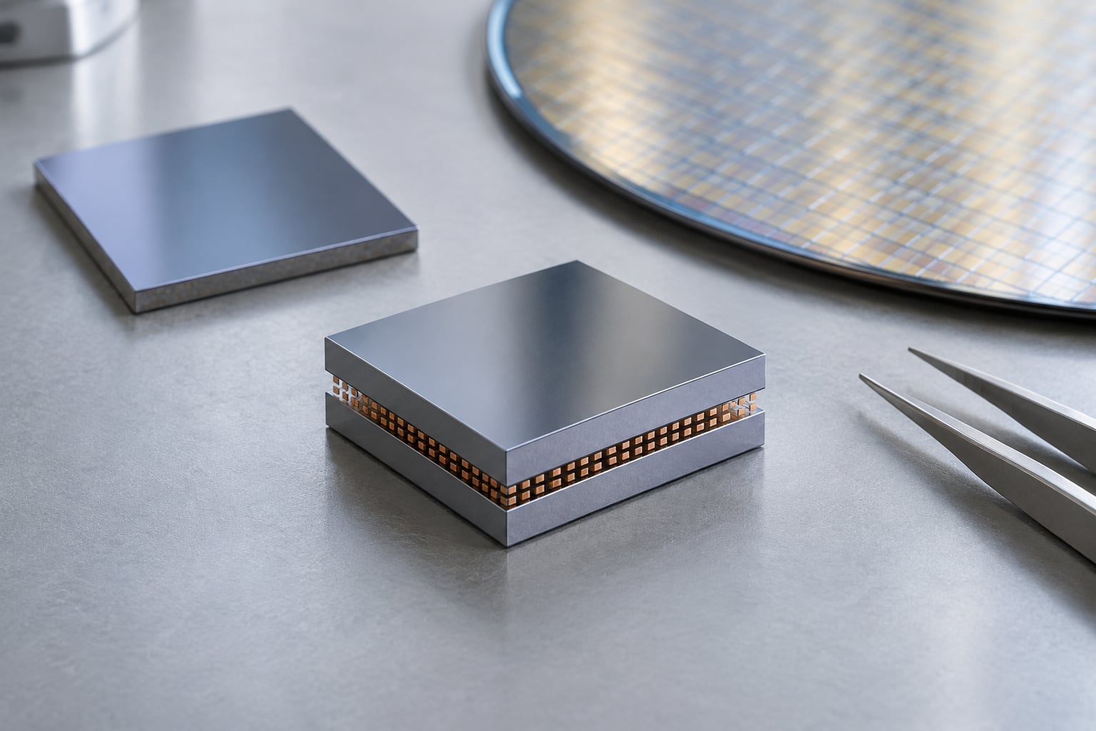
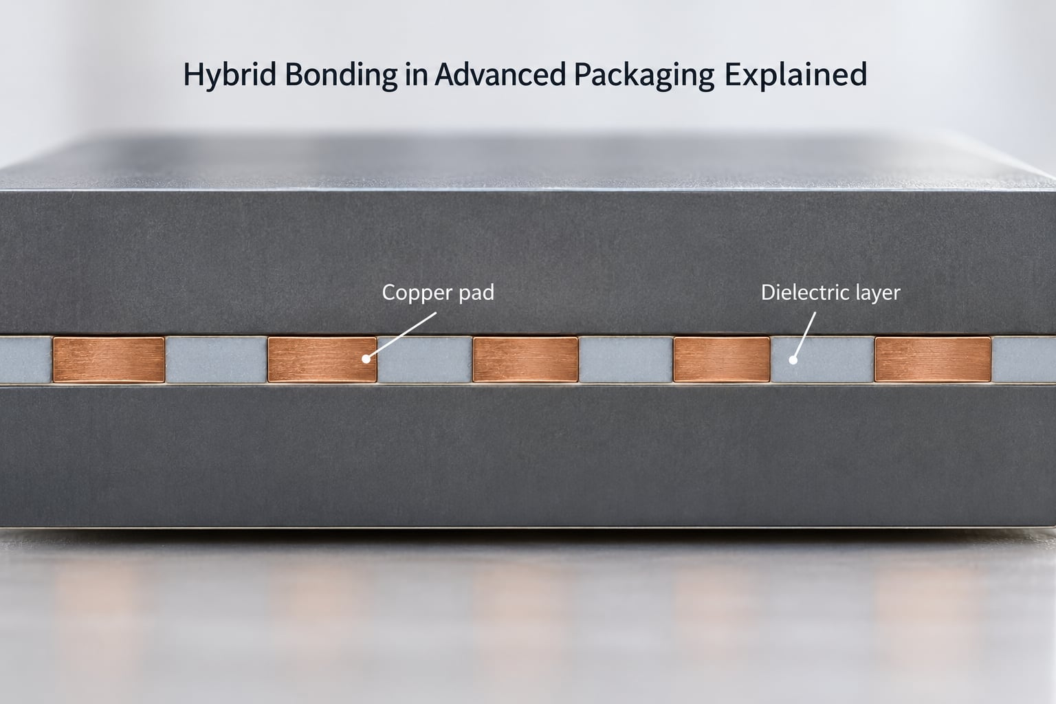
Hybrid bonding permanently fuses two prepared surfaces together. A copper interconnect on one side lands on a copper interconnect on the other, while a surrounding dielectric layer bonds to the dielectric layer opposite it and holds the whole stack in register. The dielectric does the mechanical work; the copper does the electrical work. Nothing reflows, nothing is pressed with a wire bonder, and there is no underfill to dispense afterwards.
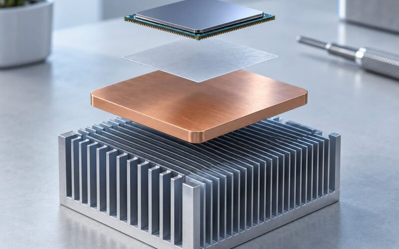
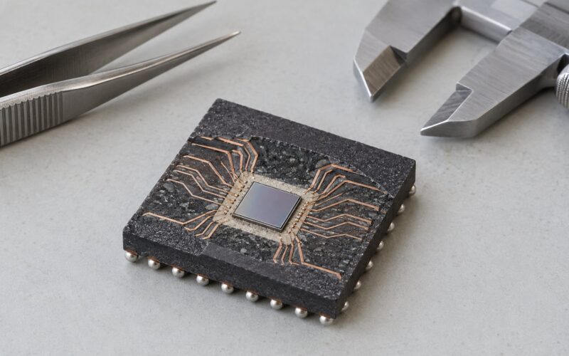
Compare that to the interconnect methods it is meant to replace. Wire bonding runs a thin metal wire from a die pad to a package lead. Flip-chip bonding flips a die face down and solders it to a substrate through bumps or balls. Thermocompression bonding presses bumps together at temperature and force, sometimes with a sintered silver column instead of solder. All three rely on a discrete piece of metal that has to physically fit between two pads, and that piece of metal sets the pitch floor.
Hybrid bonding removes the piece. The two copper surfaces touch and grow into one another, so the limiting dimension becomes the width of a lithography feature rather than the diameter of a solder ball. That single change is why the technology shows up wherever interconnect density has become the problem.
How Is Hybrid Bonding Different From Fusion Bonding and Direct Bonding?
The three terms get tangled, so it is worth separating them. Fusion bonding and direct bonding both describe joining surfaces without a filler metal, and the words are often used as synonyms. Hybrid bonding is the specific case where a dielectric bond and a conductive bond are made at the same time on the same interface.
| Term | What gets joined | Electrical path | Where you see it |
|---|---|---|---|
| Direct bonding | Two like surfaces, oxide to oxide or metal to metal, with no filler | Separate step, or none at all in pure oxide-to-oxide bonding | Research literature, some stacking flows |
| Fusion bonding | Chemical bonds between activated surfaces, usually oxide to oxide | Metal interconnect formed separately | Wafer bonding, 3D NAND stacking flows |
| Hybrid bonding (DBI) | Dielectric bonds and copper contacts formed in one anneal | Copper-to-copper, formed by the same thermal step | Image sensors, chiplet stacks, 3D logic |
Direct bond interconnect, or DBI, is the name most process engineers use for the hybrid flow. If a paper says direct bonding and then describes copper pads meeting during the anneal, it is describing the same thing you will build in a fab. If it describes only oxide bonding with no metal, it is not, and the interconnect has to be added another way.
Hybrid Bonding in Advanced Packaging Explained
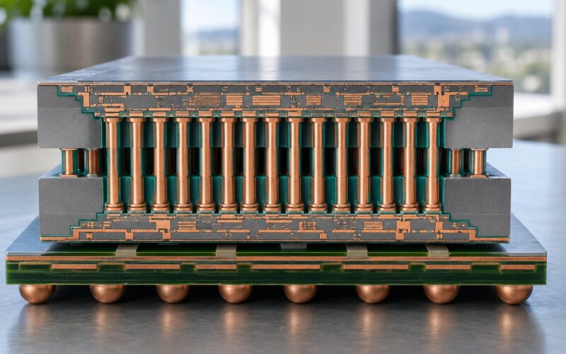
The core idea is that the interconnect stops being an object and becomes an interface. In a soldered stack, current travels down through a ball, across a solder joint, and back up into a redistribution layer. Every one of those transitions adds resistance, capacitance and inductance, and every ball consumes z-height. In a hybrid bond, current crosses a metal-to-metal contact a few hundred nanometres across, with the dielectric immediately beside it and no solder chemistry anywhere in the path.
Two details make that work. The first is the dielectric. Silicon dioxide deposited or spun onto the bonding surface, then polished flat, gives you a surface smooth enough that two oxide layers can fuse at low temperature once they are activated. The second is the copper. Copper is recessed a few nanometres below the surrounding dielectric so that, after the surfaces contact, copper expands slightly during the anneal and presses outward into its copper partner.
Fine pitch is the whole point of that geometry. Microbumps in production flip-chip work sit at 25 to 50 micrometres, and thermocompression bonding has pushed the practical floor to around 10 micrometres before bridging and coplanarity problems dominate. At those numbers a routing layer on the logic die has to get longer and longer to fan signals out from a shrinking bump field, and that routing eats power, area and signal integrity. The pitch-vs-routing penalty is why a fan-out physical layer costs energy on every bit moved.
Hybrid bonding addresses a specific set of packaging problems: interconnect density when the bump pitch is exhausted, power delivery to compute and memory tiles, signal integrity on long high-speed links, vertical interconnect height in tall stacks, and the ability to build 3D architectures that would buckle or overheat with soldered joints. It is not the answer to a package that has twelve I/O and plenty of room.
| Property | Hybrid bonding | Typical micro bump or TCB |
|---|---|---|
| Definition | Permanent dielectric plus metal bond formed in one flow | Soldered or sintered metal column between two pads |
| Bonding mechanism | Surface activation, contact, thermal anneal | Reflow or force and temperature at the joint |
| Typical pitch | Below 10 micrometres, scaling toward a few micrometres | 25 to 50 micrometres for flip-chip, about 10 micrometres for TCB |
| Interconnect density | Above 100,000 bonds per square millimetre | Thousands of joints per square millimetre |
| Main advantage | No solder, no underfill, low parasitics, small z-height | Mature, forgiving, high-volume |
| Main limitation | Demanding surface control and contamination budget | Pitch floor, solder fatigue, routing overhead |
How Hybrid Bonding in Advanced Packaging Works
The flow is deliberately boring once you accept that nothing is being pressed together. Every step exists to make two surfaces behave like one continuous surface.
1. Planarize the surface. Chemical mechanical polishing takes the wafer to a flatness and roughness target that a bonding interface can survive. The commonly cited figure for an oxide bonding surface is an average roughness below 1 nanometre. Peaks of a few nanometres are enough to open voids, because a void is simply somewhere the two surfaces never touched.
2. Form the dielectric and copper pads. The dielectric layer is deposited or coated over the metal, then patterned and etched back so copper pads are exposed. Copper itself is typically filled by electrochemical deposition after an adhesion and barrier layer. Filler uniformity matters because voids left inside a pad become voids in the bond.
3. Recess the copper. A selective polish or etch pulls the copper a few nanometres below the dielectric surface. It sounds trivial and it is the step people underestimate: the dielectric is what sets bond initiation, and the recess is what leaves room for copper to expand and make contact during the anneal. Get the recess depth wrong and you get either voids at the copper interface or a dielectric that never fully bonds.
4. Activate the surfaces. A low-energy plasma, typically an oxygen or hydrogen treatment, cleans the bonding surface and leaves it chemically reactive. The bonding face is hydrophilic afterwards, which is what makes step 5 possible.
5> Hydrate the surface. A deionised water treatment or controlled humidity exposure adsorbs a controlled layer of water molecules on the activated oxide. The van der Waals and hydrogen bonding across that layer are what hold the two dies together at contact temperature. This is why queue time between activation and bonding matters so much. Activation decays, and a surface that sat in the queue too long bonds worse than one that was fresh.
6. Align and make contact. Placement brings the two surfaces together in register. The published tolerance for production placement accuracy sits near 0.2 micrometres, which is tight for a pick-and-place style motion stage. Contact pressure is light, on the order of what a compliant mechanism can apply evenly across a die.
7. Anneal. A controlled thermal cycle, usually a few hundred degrees, drives the fusion. Water-mediated bonding completes at relatively low temperature, and copper expands into copper, creating a metallurgical joint with no liquid phase and therefore no intermetallic compound. Current high-volume flows target temperatures in the 300 to 400 degree Celsius range with cycle times measured in tens of minutes.
8. Inspect and test. Void detection is the hard part and gets its own section below. Electrical screening then separates good stacks from scrap, which matters enormously for cost in die-to-wafer work.
Configurations differ mainly in what is being placed and when.
| Configuration | What moves | Strength | Constraint |
|---|---|---|---|
| Wafer to wafer (W2W) | Whole wafers bond together | Fastest, best alignment repeatability, lowest cost per bond | Both sides must be good; one bad die loses the wafer |
| Die to wafer (D2W) | Singulated known-good dies placed on a wafer | Keeps known-good die economics, enables heterogeneous integration | Placement accuracy, throughput, coplanarity across the placed die |
| Chip to wafer (C2W) | Small die or tile placed on a wafer | Scales to fine tiles, high density per unit area | Pick-and-place speed, particle sensitivity at small die size |
| Die to die (D2D) | Two packaged or singulated dies bond face to face | Assembles parts that were never on the same wafer | Handling, warpage, cost per stack |
Wafer-to-wafer is where the economics sit today because the whole surface is bonded in one cycle. Die-to-wafer is where the roadmap sits, because it lets a manufacturer stack only dies that already passed test, and because chiplet designs need dies from different process nodes and different sources.
Why Engineers Are Using Hybrid Bonding
Pitch and density. When a compute tile needs more I/O than a 10 micrometre bump grid can offer, you have three choices: grow the die, add a second routing layer, or move to a finer interconnect. Hybrid bonding takes the third option, and it changes the arithmetic of the whole package. Above 100,000 bonds per square millimetre, the interconnect stops being the thing that limits the design.
Lower resistance and parasitics. A solder joint has resistance, and a bump plus its landing pad and routing layer add capacitance and inductance. A short copper-to-copper contact replaces that stack. On long links between memory and compute, cutting the interconnect parasitics improves signal integrity margins and reduces the power burned in I/O drivers.
Power delivery. This one gets under-discussed. A wide bump field is a decent current conductor, but a dense fine-pitch copper mesh of the same footprint carries more current with less loss, and it can be distributed across the whole die face rather than concentrated in a ring. For a data-centre accelerator, power delivered per square millimetre of compute is often a harder constraint than clock speed.
Z-height. A stack of logic die, memory and interconnect adds up fast. Bumps and underfill contribute vertical height; a hybrid bond contributes essentially the thickness of the dielectric. For a package that must fit a height budget, or a phone or a laptop, that saved millimetre is worth real money.
Thermal behaviour. Removing underfill removes one of the worst thermal resistors in the stack, because epoxy underfill conducts heat poorly. Fewer interfaces between die and heat spreader means a lower junction temperature at the same power. A lower junction temperature also buys reliability margin, which matters when the stack is eight or twelve dies tall.
3D integration. Fine-pitch bonding is what makes logic-on-logic and logic-on-memory stacks practical. It removes the routing penalty that previously forced designers to keep logic dies in a single plane, and it is the enabling step for architectures that split a processor across dies built on different nodes.
The pitch history helps frame where this lands. Flip-chip microbump pitch sat in the 25 to 50 micrometre range. Thermocompression bonding pushed to roughly 10 micrometres. Intel has described Foveros Direct generations at about 9 micrometres and then 3 micrometres, TSMC splits its SoIC offering into finer and coarser pitch variants, and research papers have demonstrated single-micrometre-class pitch in controlled conditions. Production numbers, not research numbers, are the ones to design against.
What Materials and Equipment Are Required?
Bonding surfaces. The candidates are silicon oxide, silicon nitride, and polymer dielectrics. Oxide is the production default because it is very smooth after polishing, bonds at relatively low temperature, and survives the thermal budget of a back end of line process. The cost is a high processing temperature, since oxide densification happens at a few hundred degrees. Polymer and photosensitive permanent bonding materials flow into a rougher surface and can bond at much lower temperatures, which is attractive for stacking already-fabricated devices, but they bring their own set of moisture, temperature and reliability questions.
The conductive interface. Copper is the practical choice because it can be recessed and filled by electrochemical deposition, expands predictably at anneal temperature, and is already the backbone of every back end of line interconnect. Gold and other metals appear in research work, but copper dominates production.
Cleanliness and surface condition. This is the constraint that decides everything else. A single particle between two surfaces, once they are in contact, becomes a defect that cannot be repaired, and hybrid bonding is often quoted against an ISO Class 3 cleanroom as the practical requirement. Coplanarity has to hold across the whole bond area, and roughness has to be low enough that the two surfaces can conform. Neither leaves much room for a process that tolerates a little dirt.
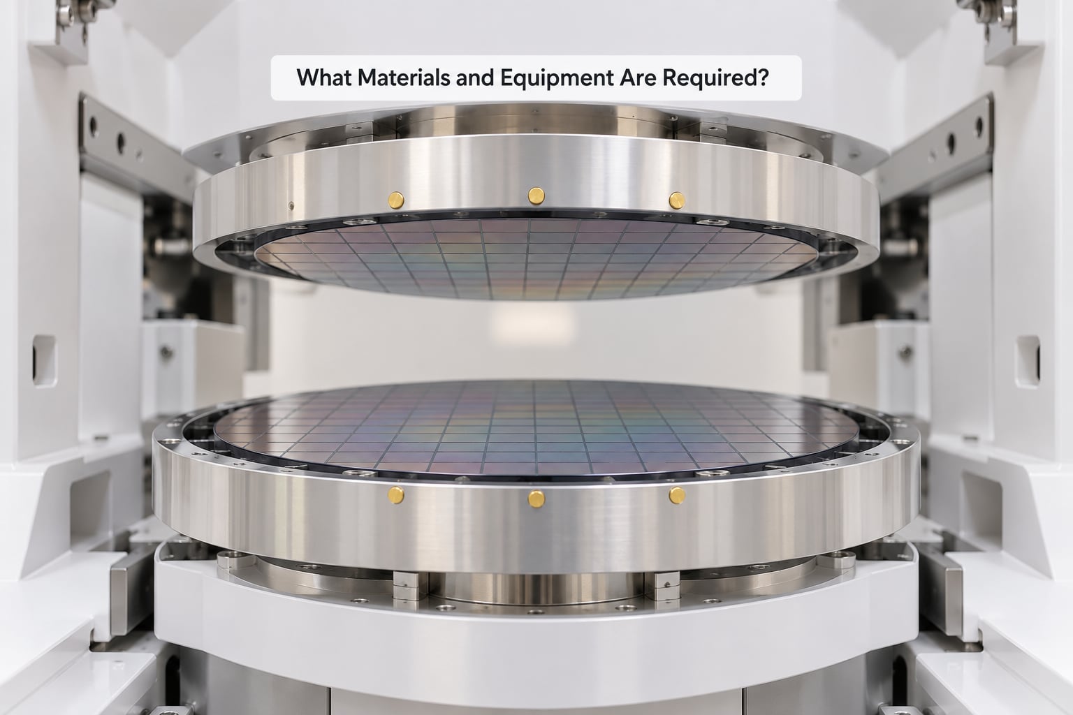
Alignment and bonding equipment. You need a placement tool with sub-micrometre overlay accuracy, ideally around 0.2 micrometres, mounted on a base stiff enough that the bond stays in registration through the anneal. The tool also has to control contact force carefully enough not to damage a thinned die. Applied Materials and Besi are two names that come up repeatedly in this market, the latter through joint work on an integrated chiplet-to-wafer bonder, and both sell toward the same argument: that the bonder alone is not enough and surface treatment and metrology have to be part of the tool.
Annealing. A controlled thermal cycle with tight temperature uniformity across the bond area, and a wet or controlled-atmosphere environment where the water layer matters. Cycle uniformity matters more than peak temperature, because a stack that bonds at 350 degrees in one corner and 380 in another has a yield problem nobody can see.
Metrology. Void inspection is the honest weak point. The resolution ladder runs from acoustic or optical methods through micro-CT and nano-CT up to TEM and FIB sectioning. Each step down buys resolution at a large cost in time, equipment and sampling, and sampling is the real problem, because a defect rate low enough to matter cannot be found by looking at a few random points. Production lines need an in-line method good enough to screen every stack, and that is the piece of the ecosystem still catching up.
Where Is Hybrid Bonding Used in Advanced Packages?
Image sensors. This is where the technology first earned its keep in volume production, and for a simple reason: a stacked backside-illuminated sensor wants the logic and the photodiode array in the smallest possible package, with no void risk near the optical path. Wafer-to-wafer fits that, because every sensor in the wafer is good before bonding.
3D logic stacking. Logic die on logic die, at 9 micrometres and finer, is what Foveros Direct and SoIC are aimed at. The requirement here is not just density but thermal: a stack that runs hot has a shorter life, so the absence of underfill matters as much as the pitch.
Memory. 3D NAND already stacks dozens of vertical layers, and the industry roadmap pushes pitch reduction further. Logic-on-memory stacks for compute-in-memory architectures are the more aggressive version, where a compute tile sits directly on a memory array and the interconnect has to carry both data and power across a large area. AMD’s 3D V-Cache parts shipped using this family of approaches on a first-generation Ryzen 7 desktop part, and those die cross-sections are the reason the topic broke into mainstream discussion, as a thread on r/Amd showed when the High Yield explainer circulated with exactly those images as evidence.
Chiplets and heterogeneous integration. Combining dies from different process nodes, sometimes different fabs, is the economic argument for fine-pitch bonding. A die-to-wafer flow preserves known-good-die economics that wafer-to-wafer throws away, and it is the flow that most of the announced chiplet roadmaps depend on.
High bandwidth memory. HBM stacks are today joined by microbumps and thermocompression bonding. The stated direction of travel is fine-pitch bonding, which would shorten the link between stacked memory and the processor, reduce the power per bit and cut the z-height of the memory stack. Whether that arrives on a given product generation depends on yield and equipment availability more than on physics.
Wafer-level and fan-out packaging. Wafer-level packaging naturally starts with intact wafers, which suits wafer-to-wafer bonding. Fan-out packaging, where a die is embedded in a moulded dielectric and further stacked, is the interesting extension, because the dielectric is already there and the surface may already be close to the flatness needed. Panel-level versions of the same idea are being discussed for cost reasons, since processing area per unit is the cost lever.
None of these are universal. A package with modest I/O, a generous height budget and a mature supply chain is better served by bumps, which are forgiving, cheap and already understood by every assembly house on earth.
Hybrid Bonding vs. Solder Bump and Other Interconnects
Compare the options on the criteria that actually decide a package architecture.
| Criterion | Hybrid bonding | Micro bump / TCB | Flip-chip | Wire bond | TSV with monolithic-style 3D |
|---|---|---|---|---|---|
| Pitch | Below 10 micrometres, scaling lower | About 10 micrometres at the fine end | 25 to 50 micrometres typical | Bond pitch of tens to hundreds of micrometres | Set by via diameter and pad geometry |
| Electrical performance | Lowest parasitics, no intermetallic compound | Solder or silver column resistance in the path | Standard, well characterised | Highest resistance and inductance | Excellent if built in the same process |
| Assembly complexity | High: cleanroom, activation, placement, anneal, inspection | Moderate | Moderate | Low | Requires a dedicated 3D process flow |
| Cost and maturity | Early in its cost curve, tooling still spreading | Mature and cheap at volume | Mature | Mature | Expensive, few sources |
| Inspection needs | Hard: void detection at nanometre scale, sampling problem | Established X-ray and SAM methods | Established | Electrical test only | Established for the process |
| Suitable architectures | Short z-height stacks, high I/O count, high bandwidth | General 2.5D and 3D, HBM today | General-purpose die attach | Low-cost packages, fine wire | Logic built in one flow, memory tiers |
The short version: solder wins on cost, tolerance and the size of the qualified supplier base. Hybrid bonding wins on density, power and z-height, and only matters when those are the binding constraints. Wire bonding is a different game entirely, kept alive by cost and by applications where fine pitch is irrelevant. Monolithic 3D integration, where the logic is built in one process rather than assembled, has the best electrical result of all and the worst flexibility, because you cannot mix process nodes or buy one part from a supplier that competes with you.
What Are the Main Challenges?
Particles and contamination. A particle between two surfaces that are about to be fused is unrecoverable. This drives the cleanroom class, the handling discipline and the cost of the facility, and it is the most cited reason hybrid bonding has not simply replaced bumps everywhere.
Coplanarity and surface roughness. Two surfaces must be flat enough, over their whole area, that they contact everywhere. Wavefront from wafer thinning, dishing and erosion from the polish step, and bow after singulation all eat into that budget. Sub-micron placement accuracy is only half the problem; the other half is the height of the die stack underneath it.
Thermal expansion mismatch. Stacking dissimilar materials means stress at the interface. Copper and silicon expand differently, a memory die and a logic die come from different process nodes with different thermal histories, and a die thinned to 50 micrometres is not mechanically forgiving. Stress shows up as warpage, as copper dishing under anneal, and eventually as delamination.
Alignment. Tightening placement tolerance has a direct cost, because at a given pitch, error eats pad area, and a pad with no margin is a pad that makes contact over a fraction of its area. The 0.2 micrometre figure is a process requirement, not a machine specification, and holding it in a volume flow is harder than the number suggests.
Voids. A void is invisible, electrically and optically, until it causes a failure. Detecting nanometre-scale voids in a large area requires expensive resolution, and the sampling statistics are brutal at high volumes. Inspection capability, not bonding capability, is the realistic gate on adoption.
Yield and known-good-die economics. A wafer-to-wafer bond is an all-or-nothing bet: a single defect anywhere affects both wafers. Die-to-wafer avoids that but inherits the cost of testing every die before bonding, plus the cost of placement, and that testing bill is the price of the process.
Low-temperature integration. Devices with thermal budgets below the bonding temperature cannot go through a conventional oxide flow. This is the entire reason polymer dielectric flows exist, and it is an active area of materials development, including work targeting lower annealing temperature and shorter cycle time.
Equipment availability and process integration. The tool set is real but fragmented. Bonders, polishers, activation and hydration modules, and inspection tools come from different vendors and are still being pulled into more integrated platforms. A line that treats them as separate islands inherits a queue-time problem at every handover, and queue time is exactly what degrades activated surfaces.
No common standard. There is still no shared interface specification or design rule set for hybrid bonding, so a chiplet designed for one flow is not automatically portable to another. For a technology meant to enable heterogeneous integration across multiple suppliers, that is a structural obstacle, and it is one of the reasons the terminology confusion has been so persistent.
Reliability qualification. Standard package reliability tests were written around solder joints and underfill. Bump-free stacks behave differently under temperature cycling and power cycling, and the models used to predict life need rework for an interface that has no solder to fatigue.
Frequently Asked Questions
What is the main difference between hybrid bonding and flip-chip bonding?
Flip-chip bonding attaches a die face down using solder balls, solder paste or sintered columns that reflow or compress at temperature. Hybrid bonding makes no solder joint at all: it fuses a dielectric layer to a dielectric layer and a copper pad to a copper pad in a single anneal. That removes the bump height, the intermetallic compounds and the underfill, and it allows pitch below 10 micrometres where flip-chip microbump pitch typically sits at 25 to 50 micrometres.
How does hybrid bonding create electrical interconnects?
Copper pads are formed on both bonding surfaces, recessed a few nanometres below the surrounding dielectric and filled by electrochemical deposition. After plasma activation and a hydration step, the surfaces are aligned and brought into contact, and a thermal anneal expands the copper into its partner, creating a solid metal-to-metal bond. The dielectric bonds at the same time, locking the alignment in place, so the copper carries current and the oxide provides mechanical strength.
Is hybrid bonding suitable for die-to-wafer and die-to-die assembly?
Yes, though the two flows carry different costs. Wafer-to-wafer bonding is the cheapest per bond and gives the best registration, but a single bad die compromises the whole wafer. Die-to-wafer and die-to-die flows place known-good parts one at a time, which protects yield economics and allows dies from different process nodes or suppliers, but they demand sub-micrometre placement accuracy near 0.2 micrometres and a much higher cost per stack. Most chiplet roadmaps depend on the die-to-wafer variant.
What are the biggest barriers to high-volume hybrid bonding?
Three barriers come up repeatedly. Surface contamination and coplanarity demand cleanroom conditions and sub-nanometre surface roughness, because a single trapped particle becomes a permanent void. Void inspection at that scale is expensive, and the sampling statistics are poor, so the in-line metrology still lags the process. Yield economics are the third: die-to-wafer flows require testing every die before bonding, which adds real cost that only density and power savings can offset.
Can hybrid bonding be used for 3D memory and logic integration?
Yes, and that is one of its main drivers. Memory stacks such as 3D NAND and future logic-on-memory architectures need interconnect density and short vertical distances that bump grids cannot reach. HBM today uses microbumps and thermocompression bonding, and the direction of travel is fine-pitch bonding to shorten the memory-to-processor link and cut power per bit. Whether a given stack generation adopts it depends on yield and tool availability more than on the underlying physics.
How do engineers choose between hybrid bonding and microbumps?
Start from the interconnect requirement rather than the technology trend. Calculate the I/O count the design needs, divide by the available die edge area, and see whether a 10 micrometre bump grid still fits once routing and power are budgeted. If it fits, bumps are cheaper, more mature and better understood by every assembly house on the supply chain. If it does not fit, or the z-height budget is exceeded, or power delivery per square millimetre is the limiting factor, hybrid bonding starts to earn its process complexity.
Conclusion: Start With the Interconnect Requirement
Decide the package from the interconnect requirement outwards. Count the I/O the design needs, work out the pitch that satisfies it, check whether the z-height budget survives the stack, and set the power and thermal budget for the join. If a 10 micrometre bump grid clears all of that, bumps are the right answer and hybrid bonding is complexity you do not need.
If it does not clear them, hybrid bonding is a genuine option, and now the real work starts: the cleanroom class, the coplanarity budget, the placement accuracy, the in-line void inspection, and the known-good-die testing that the yield model depends on. Get those five right and the bond itself is the easy part.