Critical dimension measurement is how a fab measures the width, height or sidewall profile of a printed feature so it can hold it inside specification. A critical dimension, or CD, is the feature dimension that sets the electrical behaviour of a device. Measurement happens by imaging the feature with electrons or light, by probing it with a scanned tip, or by inferring its size from how it scatters or reflects a beam, then comparing the result to the process target.
The work sounds simple until you account for what is actually being asked. A line that is nominally 20 nanometres wide cannot be measured to 20 nanometres, because no tool can resolve an edge that sharply. What a fab really wants to know is whether that line is inside a band tight enough to keep transistor drive current, leakage and interconnect resistance on target. That is a question about bias, uncertainty and sampling, not just about magnification.
This guide walks through what CD metrology measures, the methods a fab chooses between, how accurate a result has to be, how sites are picked across a wafer, and how the numbers get turned into process corrections. It is written for process, integration and metrology engineers, and for mask shops working on the same features from the other side of the print.
Table of Contents
- What Is Critical Dimension Measurement?
- Why Critical Dimensions Matter in Semiconductor Manufacturing
- How Critical Dimension Measurement Works
- Which Critical Dimension Measurement Methods Are Used?
- Optical CD-SEM: The Semiconductor Industry Workhorse
- When to Use Electrical CD or Optical Profilometry
- How Accurate and Repeatable Must a CD Measurement Be?
- How Are Critical Dimensions Sampled Across a Wafer?
- How Is CD Data Used for Process Control?
- What Are the Most Common Critical Dimension Measurement Errors?
- Frequently Asked Questions
- What is the difference between CD metrology and overlay metrology?
- Is optical CD-SEM destructive to semiconductor wafers?
- How is CD-SEM calibration performed?
- What is the difference between CD accuracy and CD repeatability?
- How many wafer sites should be measured for process control?
- Conclusion
What Is Critical Dimension Measurement?
Critical dimension measurement is the metrology process of measuring the width, height or profile of a patterned feature on a wafer, photomask or other precision part, and reporting it as a number that can be compared against a specification. Tools find the two edges of a feature, convert them into a distance, and apply a calibrated model to return line width, space width or feature height. Fab metrology engineers use it to keep lithography and etch inside their control limits.
The words get used loosely, so it is worth being precise about what sits next to CD measurement and what does not.
- CD measurement answers how wide, tall or steep a single feature is.
- Overlay metrology answers how well one layer lines up against the layer below it, in nanometres of registration error.
- Profile measurement answers about sidewall angle, bow and footing, which a two-edge width measurement cannot see.
- Film metrology answers how thick a deposited layer is.
Getting this distinction right matters because a tool, a recipe and a sampling plan built for CD will not give you overlay or profile data. In-line CD tools are also the highest-volume measurement in a fab, which is why they get the most attention from process engineers.
A short glossary covers most of the vocabulary that follows.
| Term | What it means |
|---|---|
| CD mean | Average measured CD across the sites sampled on a wafer or lot. |
| CD uniformity | Spread of measured CD across sites, wafer to wafer, or field to field. |
| 3-sigma | The CD mean plus or minus three standard deviations of the sampled data, used as a process capability band. |
| LER and LWR | Line edge roughness and line width roughness: the wobble of an edge and the resulting variation in width along its length. |
| LCDU | Local CD uniformity: variation between neighbouring elements of a repeated structure such as a contact hole array. |
| EPE | Edge placement error: the distance a printed edge misses its intended position. |
| CD bias | The systematic offset between the measured CD and the true CD, usually caused by how the tool models an edge. |
| In-line, at-line, off-line | Where the measurement happens relative to the process: in the bay near the tool, immediately after it, or in a separate lab. |
Why Critical Dimensions Matter in Semiconductor Manufacturing
A CD error is not a cosmetic defect. It changes resistance, capacitance, current and speed, and it changes them in opposite directions depending on which way the error goes. A gate that prints narrow has higher resistance, lower drive current and slower switching. A gate that prints wide adds gate-to-drain overlap capacitance and raises leakage through the channel. The process window that separates the two is narrow, and it narrows with every node.
The effect compounds through the rest of the device. Interconnect line width sets resistance per unit length on every signal and power path. Contact and via holes set contact resistance and, when they print small, the reliability margin that decides whether a die passes its burn-in. Where a structure has several walls, a per-wall variation of a fraction of a nanometre adds up faster than engineers expect.
Layout engineers mark a small number of features as critical, and those features are what CD metrology is built to watch.
| Feature | Typical critical dimension | Manufacturing risk |
|---|---|---|
| FinFET fin width | Approximately 25 nm in the widely cited 2016 in-line study, with fins around 60 nm tall | Sidewall CD sets fin capacitance and current drive; roughness along the fin hurts drive current directly |
| Gate electrode | Tens of nanometres, tightening with each node | Drives drive current, leakage and threshold voltage; tolerance is a few nanometres |
| Contact hole | Sub-100 nm and shrinking toward tens of nanometres | Small holes raise contact resistance and open the hole on etch resist mismatch |
| Metal line | Hundreds of nanometres in wide nodes down to tens in the tightest | Resist resistance per length and, in tall layers, sidewall profile affects electromigration |
| Fin or nanosheet height | Tens of nanometres, measured as a 3D dimension | Height errors change effective channel length and gate capacitance |
Those numbers describe reported structures rather than a specification for any process. Real targets live in a process integration document and change as a node matures, and no table can substitute for them.
How Critical Dimension Measurement Works
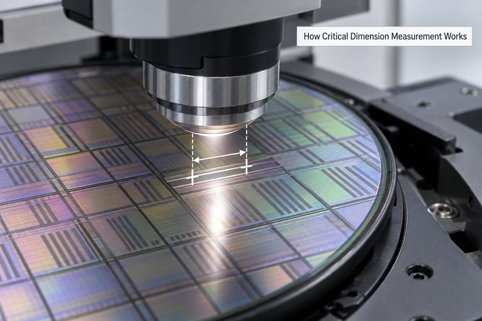
The measurement loop follows the same path whichever tool sits in it. A wafer arrives with a layer step number, a product and a slot in the tool recipe book, and the tool moves to a coordinate, finds focus, acquires the signal, extracts edges and returns a number. Everything else around that loop decides whether the number can be trusted.
- Specification. The integration team defines the CD target, the tolerance band and the response action. Without a written specification there is nothing to compare against, and the loop degrades into data collection.
- Sampling. The recipe selects sites: which fields across the wafer, how many dies, and which pattern in the die. Site count is a compromise between statistical confidence and tool cycle time.
- Focus and feature find. The tool searches for the feature it expects to see. A failed search is reported as a missing-feature code, not as a CD value, because a zero-width line and an absent line look the same to a pixel.
- Signal acquisition. A beam scans the feature. An electron-beam tool collects secondary electrons and scattered electrons; an optical tool collects scattered and reflected light; a profilometer traces height with a tip or an interferometer.
- Edge detection and calculation. The tool fits edges to the signal profile and applies an algorithm, for example a threshold or an Airy-type model for optical CD, to convert edge separation into a CD in nanometres.
- Statistical evaluation. Site results are averaged, the range and standard deviation are computed, and 3-sigma values are published for the wafer and the lot.
- Feedback. The control system compares the result to the limits and either continues running the recipe, applies a correction such as a focus or dose offset, or holds the lot for disposition.
A worked example makes the arithmetic concrete. Suppose a gate line is targeted at 40 nm with a plus or minus 1.5 nm band. Twenty-one sites across three fields return a mean of 40.3 nm with a standard deviation of 0.6 nm, giving 3-sigma values of 38.5 nm and 42.1 nm, both inside the band. The same wafer with a mean of 37.4 nm sits below the lower limit and triggers a hold even though every individual site measurement looks reasonable.
That is why CD work is a statistics problem wearing an instrumentation coat. The tool can be excellent and the process still be out of specification.
Which Critical Dimension Measurement Methods Are Used?
Four measurement principles cover nearly all semiconductor CD work, and the choice is a trade between resolution, throughput, destructiveness and what kind of structure you are pointing at. No single technique wins on every axis.
| Method | Principle | Typical resolution | Speed | Strengths | Limitations | Best use |
|---|---|---|---|---|---|---|
| Optical CD-SEM | Electron beam scanned over the feature; secondary and backscattered electron intensity plus scattered-light signal, edges found from the profile | Sub-nanometre repeatability on isolated lines | Slow, seconds to tens of seconds per site | Highest resolution and sensitivity; the reference method for resist and etched layers | Charging on insulating films, sensitivity to material and resist composition, possible resist damage at high dose, low throughput | Litho track and post-etch CD on gate, fin, metal and contact features |
| Optical CD | Coherent or broadband light, edge detection on the scattered light signal with a physical model | Sub-nanometre for isolated, well-behaved lines | Fast, milliseconds per site | High throughput, non-destructive, usable in-line on many sites, much lower cost per measurement | Model-dependent, degrades on complex 3D structures, confounded by material and colour, needs cross-tool matching against a reference | Rapid uniformity screening, resist and hard-mask lines, big products where volume matters |
| Electrical CD | Fabricate a test structure and measure its resistance or current, then infer CD from a calibrated electrical model | Set by the structure design, not by imaging; often several nanometres | Slow overall, but the value is a true electrical result | Measures what the device actually does; insensitive to optical model error; catches resistance and leakage problems end to end | Only works on structures designed for it, needs long cycle time through the fab, averages over the whole structure | Interconnect and via resistance, contact resistance, process monitors, mask and resist qualification |
| Inline optical profilometry | Interferometric or confocal height measurement, tracing the cross-section and fitting a profile model | Around a nanometre in height, weaker laterally | Moderate | Three dimensional result including sidewall angle, footing and bow; non-destructive for most films | Best on smooth, high-aspect-ratio structures, weaker on rough or collapsing lines, tip or stage artifacts on fragile features | Fin and nanosheet height, resist profile, sidewall angle, high-aspect-ratio structures |
Electron-beam scatterometry and multi-beam instruments sit between the CD-SEM and the optical tools, trading cost per site for reference-grade accuracy over large areas. Spectroscopic ellipsometry and scatterometry infer CD from how a structure changes the polarisation or angular distribution of reflected light, which is fast but heavily model dependent.
Optical CD-SEM: The Semiconductor Industry Workhorse
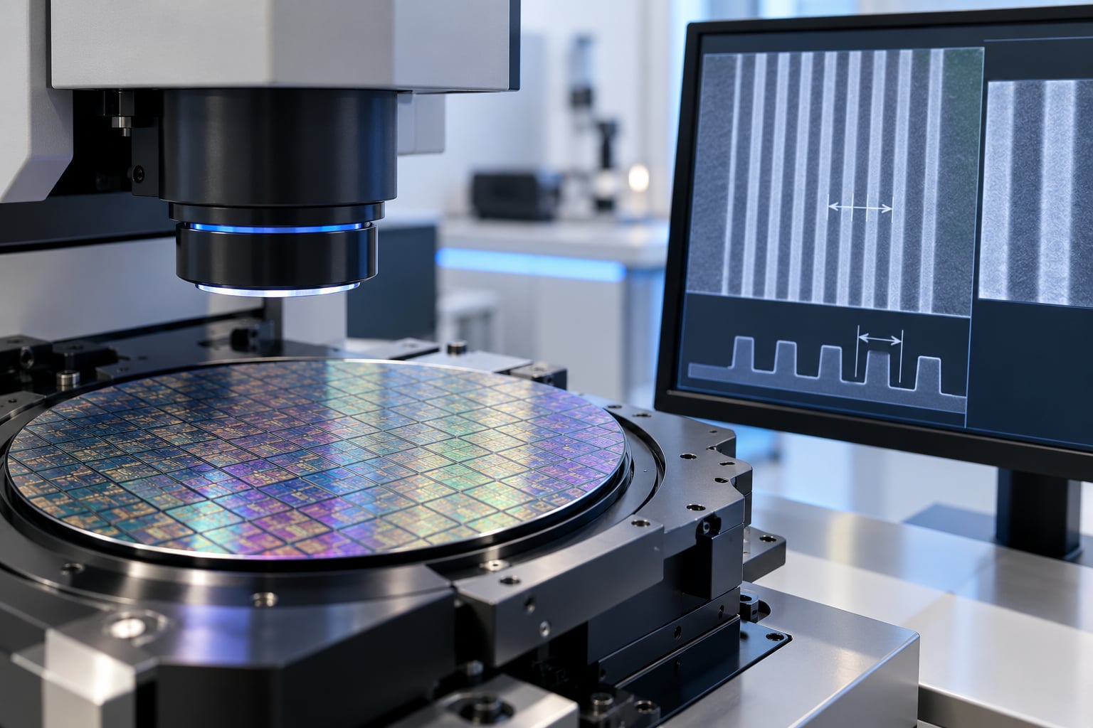
Despite the name, most production CD-SEMs are optically assisted. A narrow electron beam is scanned along a line across the feature, and the tool records two signals at once: the secondary electron image, which shows where the material edge is, and the scattered electron signal, which forms an interference-like peak whose shape carries the edge position and the profile information. The tool fits a model to that peak, which is why the same feature can measure differently on two CD-SEMs with different fitting algorithms.
Calibration is what keeps the fleet consistent. Reference standards with dimensions traceable to a national metrology institute are measured at defined intervals, and a fit of measured signal against reference value gives the tool’s bias and gain. Cross-tool matching studies then compare a shared sample set across the fleet to find the offsets that calibration alone does not remove. A newly installed tool is not assumed to match; it is proven to match.
The weakness is material sensitivity. The scattered electron signal depends on atomic number and on how the material behaves under the beam, so the same fitting recipe can read differently on a silicon line, a metal line and a resist line. Charging builds on insulating films and distorts the edge profile until the algorithm reports a width that looks fine and is not. Engineers control this with a carbon or conductive polymer coating, lower beam energy, and a site recipe validated per layer.
At advanced nodes the tool still does the reference work, even when most routine production sampling has moved to optical CD, because somebody has to tie the fast tool back to a reference. The pattern of use that has settled across the industry is optical CD for volume screening and excursion detection, with CD-SEM for recipe qualification, cross-tool matching and arbitration of a disagreement.
When to Use Electrical CD or Optical Profilometry
Electrical CD earns its place when the question is about electrical behaviour rather than geometry. A resistance monitor fabricated in the same layer as the line you care about responds to the real width, the real sidewall and the real contact resistance together, so a good number on the CD tool and a bad resistance on the monitor together tell you the process changed in a way the CD model cannot describe. That combination is a standard trigger for moving from a fast optical tool to CD-SEM or profilometry.
Mask and resist work leans the other way. A photomask blank is inspected with mask-plane and wafer-plane metrology before it ever reaches a scanner, and actinic inspection at the working wavelength is used for reflective masks because the absorber stack behaves differently at the wavelength that will print it. For resist characterisation, profilometry is preferred when you need to know sidewall angle and footing, because those two numbers drive how the layer below will be printed after etch.
Three-dimensional structures are the third case. Fins, gate-all-around nanosheets, deep trenches and tall metal lines have more than two edges, and a two-edge width model gives a confident answer that describes only the part of the profile it can see. Profilometry or scatterometry is the honest choice there, and fabs typically run a mix so the fast tool’s screen result can be cross-checked against a three-dimensional one.
How Accurate and Repeatable Must a CD Measurement Be?
Not all processes need the same answer, so this section separates the terms first and the budget second. Accuracy is closeness to the true value, and it is established by comparison against a reference standard. Precision is how tightly repeated results cluster. Repeatability is precision on one tool in one session with one recipe. Reproducibility is precision across tools, operators, labs or time. Resolution is the smallest change the tool can report at all. Bias is the systematic difference between the measured value and the true value, and it is the term engineers use most when a fab disagrees with itself.
The practical constraint is the tolerance. A measurement process is fit for purpose when its expanded uncertainty is a small fraction of the tolerance band it has to protect. If the band is plus or minus 1.5 nm, a measurement with 1 nm of uncertainty consumes most of the budget before the process moves at all.
| Uncertainty component | Typical effect | How to reduce it |
|---|---|---|
| Tool precision, short term | Repeat spread across repeated measurements of the same site | Average more sites, tighten the recipe, fix focus and threshold settings |
| Bias to a reference | Consistent offset between tool result and true value | Calibrate against traceable standards, run a correlation study per tool and per layer |
| Material and signal model error | Layer-dependent offset, especially on new materials | Validate the model per layer, compare against a reference method on a correlation wafer |
| Sampling error | Result changes when the site set changes | Increase site count, choose sites that span the process, randomise within a field |
| Focus and feature placement | Edge signal shifts when the beam sits on a different part of the profile | Fix focus per layer, verify the feature-find window on each run |
| Charging and contamination | Progressive drift through a scan | Coat insulating films, adjust beam energy, clean the chamber, monitor drift charts |
| Resist damage and beam exposure | Measurement itself changes the feature at high dose | Use the lowest dose that reaches the required signal to noise, verify with dose ladders |
| Environment | Temperature, vibration and floor motion on high-precision tools | Monitor vibration and temperature, keep the tool on a proper foundation and isolated slab |
None of these components matters if the sampling is wrong. Adding sites reduces sampling error but does nothing about bias, and tightening the recipe reduces precision error but does not remove a model that is wrong for the material. Good programs attack the component that is actually largest, which is usually determined by a correlation study rather than by opinion.
How Are Critical Dimensions Sampled Across a Wafer?
Sampling is where CD programs most often fall short. A wafer carries tens of thousands of identical dies and a tool can measure a few hundred sites in the time available, so the site list has to be designed to answer the question being asked. Three levels of sampling exist, and most production recipes use all three at once: die level decides which die is measured, wafer level decides where on the wafer those dies sit, and lot level decides how many wafers out of the batch get measured.
Site placement matters as much as site count. A cluster of sites in one field tells you about one field and nothing about the wafer, because exposure and etch gradients are spatial. At minimum, the wafer map should cover the centre and the edge, and for tools with a known radial signature it should include several radii rather than a scatter. Edge exclusion rules follow from this: the outermost few millimetres behave differently for good physical reasons, and including them without treating them separately adds noise that looks like a process shift.
| Strategy | What it looks like | Use it for | Trade-off |
|---|---|---|---|
| Fixed grid | Same coordinates on every wafer in the lot | Long-term process trending, comparing wafer to wafer | Misses a small defect unless the site set happens to hit it |
| Edge and centre split | More sites at the edge, fewer in the middle | Detecting edge-driven etch and focus signatures | Centre behaviour is estimated from too few points |
| Radially distributed | Sites at several radii and azimuths | Ring and radial non-uniformity tracking | Fewer points per individual radius |
| Randomised within field | Random offsets inside a fixed field | Avoiding systematic aliasing with the pattern layout | Less repeatable site to site, so more sites are needed |
| Lot-level subsampling | A few wafers per lot measured, the rest by proxy | Cost control on long, stable processes | An excursion between measured wafers can pass unseen |
| Adaptive screening | A fast full-wafer pass, then slow measurement only where the fast pass flagged | High-volume lines with a fast optical tool available | Only works if the fast pass and the reference method agree |
The statistical limit is worth stating plainly. CD data is sparse by design, so a shift confined between sample sites is invisible to statistical process control no matter how many sites were measured on that recipe. That is why excursion detection relies on sampling deliberately placed where failures have historically appeared, and why periodic reseeding of the site map is a normal part of program maintenance.
How Is CD Data Used for Process Control?
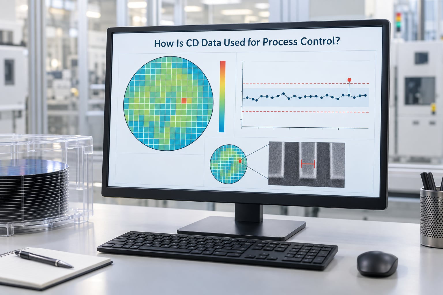
A CD measurement only becomes process control once it is wired into a loop with limits and a response. The loop has four parts: a target, a limit set derived from process capability, a rule that says who does what when a limit is crossed, and an owner who investigates. Fabs run two limit sets, warning and specification. Crossing the warning limits triggers a review; crossing the specification limits triggers a hold and a disposition decision.
Data usually lands on control charts, one per layer, per feature, per tool or per tool group. Points inside the limits are common-cause variation and only mean the process is stable. A point outside them is a signal, and the investigation starts with the simplest explanations: a new lot of resist, a tool PM, a reticle change, a focus shift, or a real process drift.
Distinguishing common-cause from assignable variation is the skill the chart exists to support. Three-sigma limits describe how the process behaves when nothing special is happening, so a single point outside them is an assignable cause worth looking for. A run of points drifting toward a limit without crossing it is a slow trend, which is more dangerous because it is easy to dismiss and often shows up in the electrical data first.
Feedback then takes one of three forms. Feed-forward corrects before the next wafer, for example a dose or focus offset applied by the control loop. Feedback corrects after the fact, for example an etch recipe adjustment based on the measured land and trench widths. Prevention stops the shift reaching production, for example a reticle hold when mask-plane data shows a defect on the plate rather than the wafer.
Process technology node moves the numbers continuously. A tool that could resolve a 100 nm line comfortably will struggle to tell a 14 nm line from a 12 nm one, and a fab that keeps the same tolerance band as it shrinks will simply measure noise. Tolerances, sample counts and reference standards all get revisited at each node transition, which is why metrology programs are versioned rather than inherited.
What Are the Most Common Critical Dimension Measurement Errors?
Most CD problems are boring and repeat well, which means they are usually caught by a check that already exists but is not being run.
- Calibration drift. The tool passes its own check but has moved away from the reference. Check the calibration trend chart and run a cross-tool correlation on a shared sample rather than trusting a single standard.
- Focus errors. A focus shift changes the edge signal and the fitting algorithm returns a plausible wrong width. Verify focus per layer after any resist or chemistry change.
- Feature charging. On insulating layers, charge builds during the scan and skews the profile. Watch for progressive drift within a single scan and apply a coating or lower beam energy.
- Resist collapse or a damaged feature. A high-aspect-ratio line narrows or tilts before etch, and a narrow-line measurement sees the collapsed line rather than the printed one. Cross-check profile before believing the width.
- Edge placement errors. The feature is there but in the wrong place. Compare the measured CD with the design intent and check overlay at the same site before calling it a CD excursion.
- Unstable background. Residue, a lifting film or a scratched substrate changes the background the algorithm fits to. Inspect the site after an out-of-family result.
- Tool matching problems. Two tools disagree because of a fitting recipe difference, not a process difference. Align the recipes and run a correlation study before changing the process.
- Poor sampling. The site set misses the region where the problem lives. When a chart shift appears with no matching process history, check the sampling plan before the tool.
The general habit that catches most of these is the same: when a result looks wrong, go look at the feature. An image, a profile or a physical check costs minutes and resolves arguments that a correlation study takes a day to settle.
Frequently Asked Questions
What is the difference between CD metrology and overlay metrology?
CD metrology measures how wide, tall or steep a feature is. Overlay metrology measures how far a layer’s features sit from their intended position relative to the layer below. A CD result answers a size question, an overlay result answers an alignment question, and a device can fail one while passing the other.
Is optical CD-SEM destructive to semiconductor wafers?
It can be. The electron beam deposits energy in the resist and substrate, so very high doses on soft photoresists can change the very line being measured. Production recipes use the lowest dose that gives an acceptable signal, and for finished wafers where damage is unacceptable, optical or non-contact profilometry is the safer choice.
How is CD-SEM calibration performed?
A reference standard with a dimension traceable to a national metrology institute is measured under the recipe that matters, and the tool’s fitting and scaling are adjusted so the result matches the reference. Standards are re-measured on a schedule, and after any change to the column, detector or algorithm. Cross-tool correlation on a shared sample confirms the fleet agrees.
What is the difference between CD accuracy and CD repeatability?
Accuracy is how close a CD measurement is to the true value, established against a traceable reference. Repeatability is how tightly repeated measurements of the same feature agree on the same tool in one session. A tool can be perfectly repeatable and still be wrong by a fixed amount, which is why both a calibration and a repeatability study are required.
How many wafer sites should be measured for process control?
Enough to separate the process variation you care about from the sampling error, and placed to cover the wafer spatially rather than clustered in one field. Fab recipes commonly use tens of sites per wafer, with extra sites at the edge and fewer in the centre. The right number comes from the tolerance band and the observed spatial signatures, not from a fixed rule.
Conclusion
The first practical step in setting up critical dimension measurement is not choosing a tool. It is writing down the feature, the target, the tolerance band and the action that follows a breach, because a measurement without a specification is just data. Once that exists, pick the method that matches the structure and the throughput need, prove its repeatability and its uncertainty against a reference, and then place it inside a documented control loop with limits and an owner. Everything else in a mature CD program, from adaptive sampling to fleet correlation, follows from those four decisions being written down and reviewed.