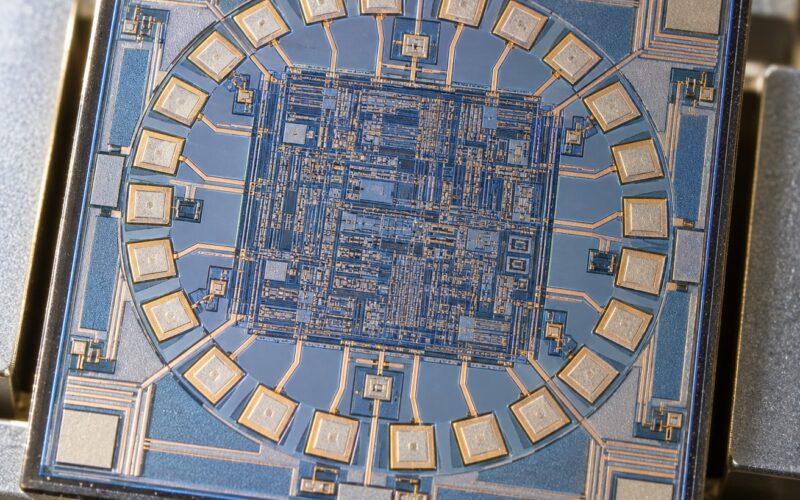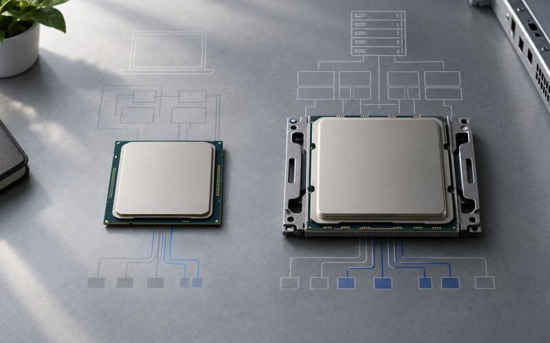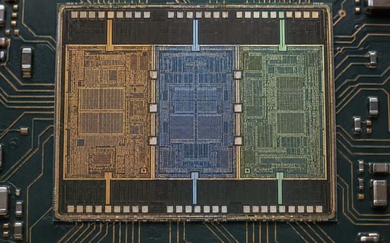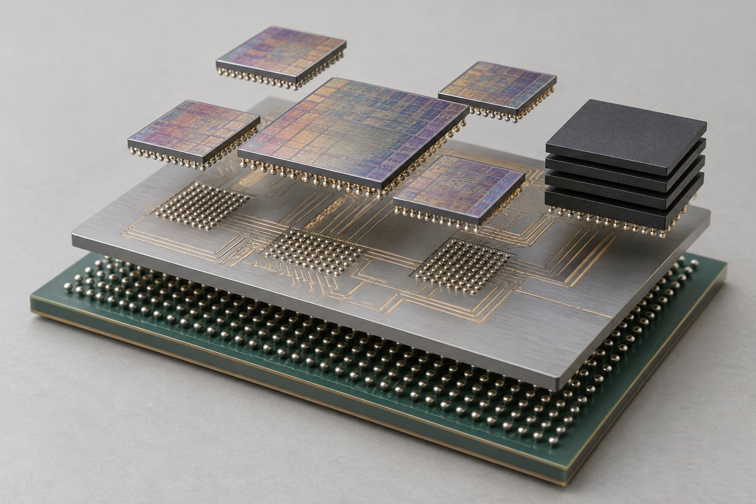
A chiplet is a small die that does one job well, manufactured separately and then joined electrically to other dies inside a single package, so the finished processor behaves to software like one ordinary chip. That is the entire concept behind chiplets explained for beginners in a single sentence: a large processor is no longer one slab of silicon, it is a small team of specialists living in the same package.
A monolithic die is one enormous block containing CPU cores, memory controllers, I/O and graphics all etched together. A chiplet package splits those same functions into separate pieces and connects them with dense on-package links. AMD’s Zen 2 desktop processors, Intel’s Meteor Lake mobile chips, Apple’s M2 Ultra and Nvidia’s Blackwell graphics chips all ship in this multi-die form.
The reason is arithmetic, not fashion. A single die cannot be printed arbitrarily large, and very large dies are expensive to make because more of them come off the wafer defective. Splitting a processor changes both of those numbers.
Table of Contents
- What Are Chiplets?
- Why Semiconductor Companies Use Chiplets
- How a Chiplet System Works
- Chiplets Explained for Beginners: From Dies to Package
- What Is the Difference Between a Core, a Die, and a Chiplet?
- How Chiplets Connect to Each Other
- What Is Chiplet Packaging?
- What Benefits Can Chiplets Provide?
- What Are the Main Challenges and Limitations?
- Which Devices Use Chiplets Today?
- How to Tell Whether a Chip Uses Chiplets
- Frequently Asked Questions
- Are chiplets faster than traditional chips?
- What is the main purpose of using chiplets?
- Do chiplet processors work like a single chip?
- Can you replace or upgrade an individual chiplet?
- Are chiplets the same thing as multicore processors?
- What to Learn First
What Are Chiplets?
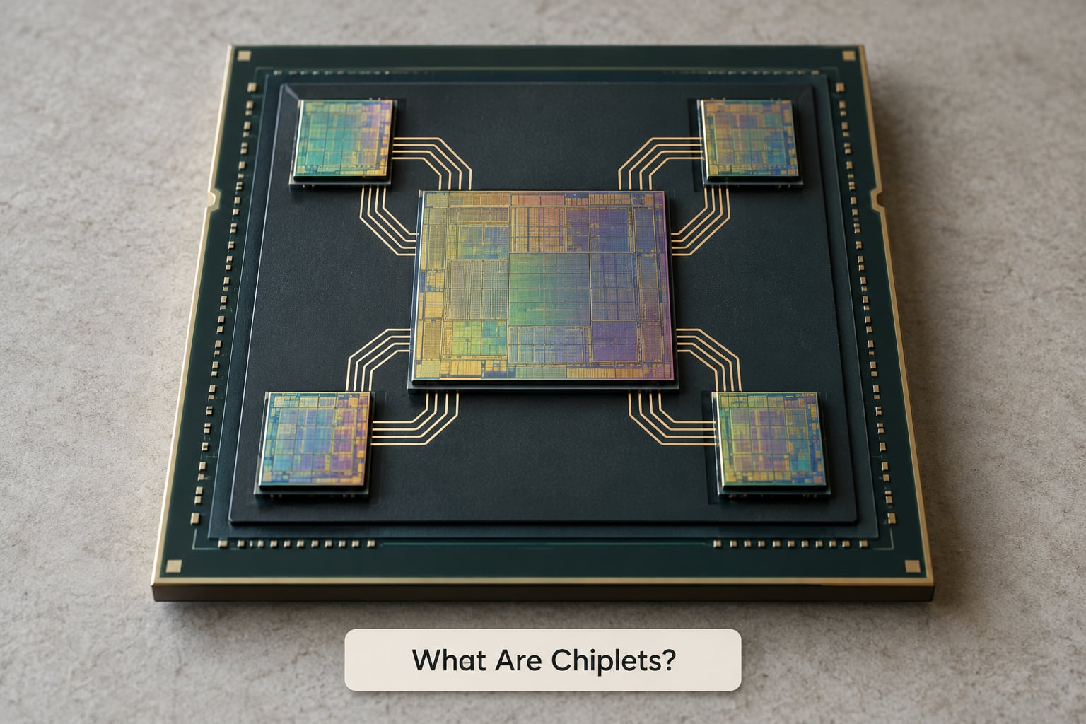
A chiplet is a die built to perform one function, then mounted with other dies in a shared package and wired to them through die-to-die links. A processor built that way is still one chip to the buyer, the operating system and every piece of software.
Manufacturers divide a design because the functions inside it do not scale at the same rate. CPU logic cores shrink well with each process node. Analog blocks, memory controllers, power management and I/O do not shrink as quickly, so forcing them onto the newest, most expensive process usually wastes area and costs power.
Splitting those functions onto separate dies lets each one sit on the process node that suits it. A compute die on a leading-edge node, an I/O die on a mature, cheap node, high-bandwidth memory beside both.
Why Semiconductor Companies Use Chiplets
Chiplets solve six practical problems, and none of them is “make the chip run faster.”
- Yield. Yield is the share of finished dies on a wafer that work. Defects scale with area, so a die covering four times the area usually yields far less than one die covering a quarter. Smaller chiplets mean more good pieces per wafer.
- The reticle limit. Lithography tools expose a rectangle of roughly 858 square millimetres at a time, so one die cannot exceed that area no matter how much money is spent. Chiplets are the practical way past a physical ceiling.
- Process node matching. Each die is fabricated at the node where that function performs best, instead of dragging legacy circuitry onto an expensive leading-edge wafer.
- Portfolio reuse. One validated compute chiplet can appear in a six-core desktop part, a 64-core server part and a 192-core server part, which spreads design cost across a whole product line.
- Parallel development. Two teams can design and verify different chiplets at the same time, then integrate them once each is finished.
- Supply flexibility. When demand for one product shifts, capacity can be directed to another combination of dies already in production.
Be clear about what does not follow. More chiplets does not mean more cores, and it does not guarantee better performance. The link between dies costs time and energy that a monolithic die does not spend, and only pays for itself when the partitioning is sensible.
How a Chiplet System Works
Inside a chiplet package, each die keeps its own function and moves data across short electrical links rather than across one giant piece of silicon. A desktop processor with two compute chiplets and one I/O chiplet is the easiest example to picture.
When a core needs data, most requests are served by cache sitting on the same compute die, so the trip stays local. When a core needs system memory, the request crosses the die-to-die link to the I/O chiplet, which owns the memory controllers, and only then reaches DRAM off the package. Some designs skip that hop entirely by placing memory controllers next to the compute cores and routing traffic locally, which is why the layout of the package matters as much as the number of dies.
PCIe lanes, USB controllers, display outputs and networking blocks usually live on the I/O die too. That is why forum regulars who lift the heat spreader off a Ryzen processor and find one small die next to two identical larger ones are looking at the whole architecture: the small one is I/O, the other two are compute.
Chiplets Explained for Beginners: From Dies to Package
Chiplets explained for beginners becomes easier once you follow the physical sequence, because each step is a separate industry with its own suppliers.
- Design partitioning. Engineers decide which functional blocks become separate dies and where the die-to-die links go.
- Wafer fabrication. Each die design is printed on its own wafer at its chosen process node, in a foundry that can make that node.
- Wafer sort. Dies are electrically probed on the wafer and binned. Ones that pass are cut apart and become known good dies, meaning each one is already tested before packaging.
- Package assembly. Known good dies are placed onto a silicon interposer or organic substrate, aligned to micron-scale accuracy, and joined with solder micro-bumps or direct copper bonding.
- System integration. The assembly is tested again as a whole, connected to the board, and shipped. From that point on, software sees a single processor.
Step three is the part beginners miss, and it is what makes the economics work. You are not gambling on a whole 800 square millimetre chip; you are assembling several smaller parts that each passed their own test.
What Is the Difference Between a Core, a Die, and a Chiplet?
These words get used interchangeably, and they describe four different things: a computing unit, a piece of silicon, a packageable function and a finished assembly. The table separates them.
| Term | What it is | Physical scope | Example |
|---|---|---|---|
| Core | One execution unit that runs instructions | Inside a die, far too small to handle or replace | A single Zen core inside a compute die |
| Die | One piece of cut silicon carrying circuitry | Square millimetres to about 858 mm2 | A compute chiplet with eight cores and its cache |
| Chiplet | A die built as one function and packaged with others | One die inside a shared package | Two compute chiplets plus one I/O chiplet in a desktop CPU |
| Package | The sealed assembly holding one or more dies | The part you actually buy and solder down | A desktop CPU, a graphics card chip, a smartwatch module |
| Monolithic die | One die containing the whole design | Approaches the reticle limit as designs grow | A single-die desktop processor |
| System-on-a-chip (SoC) | An integrated design containing many functional blocks | One die, though it may itself be made of chiplets | A phone system-on-chip with CPU, GPU and modem blocks |
| Multi-chip module (MCM) | Several dies bonded onto a common substrate | A package holding several dies | A chiplet package wired to a shared substrate |
| System-in-package (SiP) | Multiple dies plus supporting components in one package | Can include memory and sensors | A watch module combining processor and memory dies |
| Tile | Vendor wording for a repeating die in a multi-die design | Often interchangeable with chiplet | Intel tiles: compute, system-on-chip and I/O tiles |
So a chiplet is not a bigger core, and a package is not a chiplet. Two chiplets holding eight cores each give you sixteen cores; one chiplet holding two cores and one I/O chiplet gives you two cores plus all the I/O.
How Chiplets Connect to Each Other
Die-to-die links move data between chiplets at speeds measured in gigabits or gigabytes per second per lane, and the choice of link shapes the whole design. Wide parallel links move many bits at once at low latency, which suits cache traffic. Long serial links move bits one after another, use fewer wires and reach further, which suits coherent traffic crossing the package.
Three numbers matter. Bandwidth is how much data moves per second. Latency is how long a hop takes, and it is usually higher than an on-die wire of the same length. Energy per bit decides how much power the package burns on interconnect rather than computation, and that share grows as more functions move off the main die.
Until recently each vendor had a proprietary link. AMD calls its fabric Infinity Fabric, Intel uses EMIB bridges and Foveros stacking, Apple describes its die-to-die connection as UltraFusion. UCIe, the Universal Chiplet Interconnect Express, is the attempt to change that. Announced in 2022 by Intel, AMD, Arm, TSMC, Samsung, Google and Microsoft, it defines a physical layer, meaning the electrical and timing rules for the connection, and a protocol layer, meaning how traffic is packaged and routed. Version 2.0, released in 2024, added support for 3D stacking and manageability features.
A useful analogy: UCIe plays the role PCIe played for expansion cards. Nobody argues that a graphics card is soldered onto the mainboard, but PCIe made mixing parts from different vendors practical, and UCIe aims to do the same thing inside the package. What it does not standardise is everything above the link, such as cache coherency between dies.
What Is Chiplet Packaging?
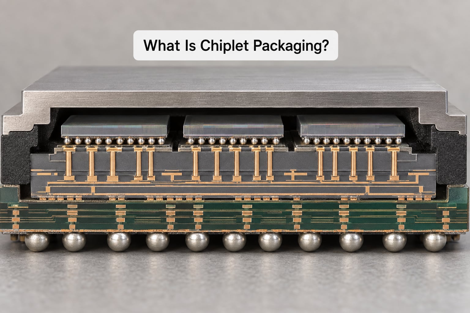
Chiplet packaging is the set of techniques that mounts dies on a common carrier and connects them electrically. The carrier is usually a thin silicon interposer, a piece of silicon carrying dense wiring, or an organic substrate, which is cheaper and less dense but adequate when dies sit close together.
A 2.5D package places dies side by side on the interposer. It suits wide pieces such as compute tiles and stacks of high-bandwidth memory, which is the arrangement used in large AI accelerators. A 3D package stacks dies directly on top of each other, which shortens the links dramatically but concentrates heat into a small volume. Hybrid bonding replaces solder micro-bumps with direct copper-to-copper contacts, allowing far tighter spacing between stacked layers.
Package assembly is hard work in its own right. Alignment has to hold to a few micrometres, thousands of connections carry power and data at once, signal integrity degrades with poor layout, and heat has to leave through the same surface the cooling solution touches. Chiplets do not make packaging easier; they move the difficulty there.
What Benefits Can Chiplets Provide?
Six benefits show up repeatedly, and each one depends on the design rather than following automatically from splitting the chip.
- Higher effective yield. Smaller dies yield better, so more of the wafer becomes usable parts. This is the clearest benefit.
- Lower cost per good part. Better yield, mature nodes for I/O and reuse across a product line all reduce what the manufacturer pays for a working processor.
- Node flexibility. Compute on a leading-edge node and I/O on a mature one cuts both die area and power.
- Modular product lines. A fixed set of compute chiplets can be combined in different counts with one I/O die, which shortens the time to launch each new model.
- Supply planning. Capacity can shift between models that share dies, and a leading-edge compute die is not tied to the schedule of a large display controller.
- Repair potential. A package that fails because of one die can sometimes reuse the good dies, though in practice most failed parts are scrapped.
Performance per watt improves mainly because the cache and I/O stop paying leading-edge prices. Raw clock speed usually has less to do with it.
What Are the Main Challenges and Limitations?
Chiplets are a tradeoff, and the costs are real. Sceptics on hardware forums are not imagining them.
| Problem | What goes wrong | How designers manage it |
|---|---|---|
| Interconnect overhead | Off-die hops add latency and energy per bit | Keep latency-sensitive structures on one die, use wide links for bulk traffic |
| Extra design work | Partitioning, link design and verification all scale up | Reusable interface blocks and standard link specifications |
| Package cost | Silicon interposers and fine-bump assembly are expensive | Reserve them for products where die savings dominate |
| Thermal density | 3D stacks concentrate heat in a tiny volume | Thicker heat spreaders, better lid materials, smarter power limits |
| Test coverage | Interconnect faults appear only after assembly | Known good die testing plus package-level test and repair features |
| Interoperability | Vendors historically used incompatible links | UCIe as an open specification |
| Poor partitioning | A split that moves frequently used data on and off dies loses more than it gains | Prototype the split and measure before committing |
Security and supply arguments come up too. A package assembled from dies from more suppliers widens the number of parties involved, and a design tied to one vendor’s chiplet cannot easily be resourced elsewhere.
None of this stops adoption, because the reticle limit does not move. It does explain why chiplets appear in server CPUs, flagship desktop parts, graphics chips and AI accelerators first, and why cheap microcontrollers and small phone chips are usually still one die.
Which Devices Use Chiplets Today?
Chiplets are concentrated in high-end computing, where die sizes are large enough to hit the reticle limit and volumes justify expensive packaging.
- Server processors. AMD’s EPYC line scales by adding identical compute chiplets around a central I/O chiplet; the latest generations reach 16 compute chiplets and 192 cores in one package.
- Desktop processors. Ryzen chips pair one or two compute chiplets with a small I/O chiplet, and Threadripper parts use the same building blocks in larger counts.
- AI accelerators. AMD’s MI300X packages eight compute dies built on four 3D-stacked I/O dies, twelve dies in total, beside six high-bandwidth memory stacks. MI300A scales further, to 24 compute dies and 128 gigabytes of unified memory.
- Graphics chips. Large GPUs reach reticle limits quickly, so designs split into several dies; Nvidia’s Blackwell generation puts two roughly 104-billion-transistor dies in each GPU.
- Mobile chips. Intel’s Meteor Lake separates a compute tile, a system-on-chip tile and an I/O tile so low-power functions avoid the most expensive process.
- Desktop and studio Macs. Apple’s M2 Ultra connects two M2 Max dies through what the company calls UltraFusion, presenting a single processor with up to 128 gigabytes of unified memory.
Two cautions. Chiplet count does not map to core count, because I/O and cache dies add no cores at all. And two chiplet processors with identical core counts can behave very differently depending on where the cache sits.
How to Tell Whether a Chip Uses Chiplets
You can usually confirm a chiplet design from public material, though the evidence varies in strength.
- Package photographs. Top-down shots of a processor often show several distinct rectangles of silicon under the heat spreader. Colour differences between rectangles are a normal artefact of different dies.
- Deck shots and die photographs. X-ray or infrared imaging reveals individual dies even when the package is sealed.
- Architecture diagrams. Vendor block diagrams that label compute tiles, I/O dies, memory dies or SoC tiles are the clearest confirmation.
- Documentation. Datasheets and technical briefs sometimes state die counts, core-to-die mappings and supported memory configurations.
- Teardowns and specifications. Review sites that remove the heat spreader and photograph what is underneath.
Watch the wording. Some vendors use chiplet and tile loosely, and a marketing claim that a chip is modular does not by itself prove several dies exist. Confirm with a package photograph or a die layout before repeating the claim.
Frequently Asked Questions
Are chiplets faster than traditional chips?
Not automatically. A chiplet processor can match or beat a monolithic design because its logic sits on a newer process node and its cache is cheaper to build, but every trip between dies costs latency and power. Chiplets help most where die size limits the design, not where a small chip already fits comfortably on one die.
What is the main purpose of using chiplets?
Manufacturing yield. Smaller dies defect less often, so more usable chips come off each wafer and the cost per working part falls. Two further motives follow from that: a die cannot exceed the roughly 858 square millimetre reticle limit, and each function can be built on the process node that suits it best.
Do chiplet processors work like a single chip?
Yes. All the dies are wired together inside one package and presented to the motherboard, firmware and software as one processor. Software developers write for a monolithic processor and do not need to know or care that the internal implementation is split across several dies.
Can you replace or upgrade an individual chiplet?
No. Chiplets are attached to the package substrate during assembly and the whole package is sealed, so an individual die cannot be swapped. Modularity exists at design time, when one compute die can be reused across several product models, not at ownership time in your own system.
Are chiplets the same thing as multicore processors?
No. Multicore describes how many computing units a processor has. A chiplet describes how those units and other functions are physically divided and connected. A processor can be multicore and monolithic, multicore and chiplet-based, or a chiplet design where some dies carry I/O or cache and add no cores at all.
What to Learn First
Study these in order and the rest of the field stops being confusing. Start with wafers, dies and process nodes, because every chiplet conversation sits on top of them. Then separate a core from a die from a package, which is the single biggest source of confusion for newcomers.
Next, learn how die-to-die links work: bandwidth, latency, energy per bit, and what a standard such as UCIe does and does not cover. After that, look at packaging, including interposers, 2.5D side-by-side layouts and 3D stacking. Only then dig into yield economics, because the yield argument makes no sense until you know how a wafer becomes a tested die.
A good exercise finishes the job. Take a labelled diagram of a chiplet package with the compute die, the I/O die, the interposer, the substrate and the memory stacks marked, then draw a monolithic die of equivalent total area beside it. Now mark every place traffic would have to cross a die boundary. That single sketch explains more than most product reviews do.
A chiplet is a die that does one job, joined to other dies inside one package. The industry moved that way because a single die hit a physical size ceiling and because large dies yield badly, and in 2026 that shift is now the default design for server CPUs, flagship desktops, graphics chips and AI accelerators.