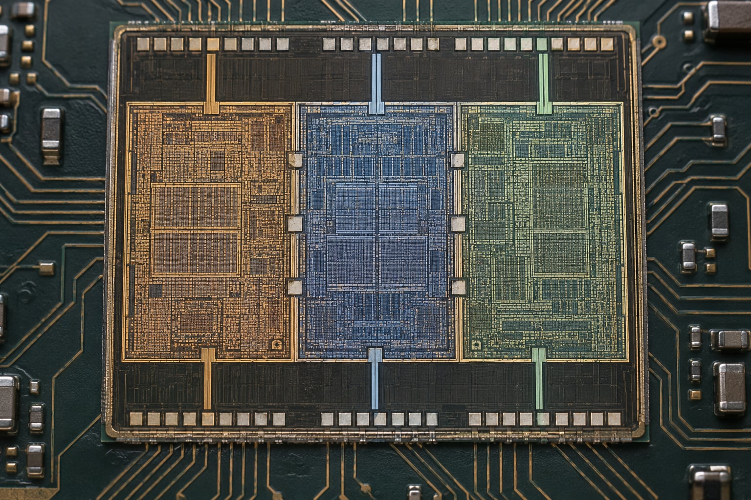
Voltage islands in SoC design are groups of on-chip blocks powered from their own supply voltage instead of the chip-wide default. Performance-critical cores run at a high VDD while slow peripherals run at a lower one, because dynamic switching power scales with the square of supply voltage. In practice, every boundary between two islands needs a level shifter.
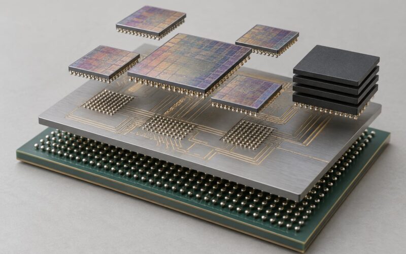
A system-on-chip compresses a processor, memory controllers, peripherals, analog and I/O onto one piece of silicon. That density is where the power problem comes from: the CPU cluster and a UART are on the same die, but they have almost nothing in common as loads.
- One supply per island. Each island draws from a named supply at a fixed voltage, set at design time rather than at runtime.
- Quadratic payoff. Cutting a rail from 1.2 V to 0.9 V removes roughly 44% of that block’s switching power.
- A cost at every boundary. Level shifter cells sit on signals crossing between islands, and each adds area and delay.
- A physical cost. Every island needs its own power grid, pads or bumps, and its own IR-drop budget.
Table of Contents
- What Are Voltage Islands in SoC Design?
- Why Do SoCs Need Multiple Voltage Domains?
- Where multi-VDD sits against the other low-power techniques
- How Does Voltage Islanding Work?
- What Happens When Signals Cross Voltage Domains?
- How Are Voltage Islands Implemented in RTL and Physical Design?
- How Do Voltage Islands Affect Power, Timing, and Area?
- What Are the Common Voltage Island Design Mistakes?
- How Do You Verify Voltage Islands Correctly?
- Where Voltage Islands Are Heading
- Frequently Asked Questions
- Are voltage islands the same as power domains?
- Can a voltage island contain blocks with different supply voltages?
- Why are level shifters needed between voltage islands?
- How do voltage islands affect timing closure?
- Does using a lower voltage always reduce total chip power?
- How can an engineer verify that all voltage-domain crossings are correct?
- Key Takeaways
What Are Voltage Islands in SoC Design?
A voltage island is a group of on-chip circuit elements powered by the same voltage source, independent of the chip-level voltage, which allows different portions of a design to run at different voltages. That is the canonical definition from the core-based SoC literature, and the rest of this article unpacks what it means at the block, cell and metal layer.
Confusing the neighbouring terms causes most of the misunderstandings around this technique, so it is worth pinning them down before going further.
| Term | What it changes | What it costs you |
|---|---|---|
| Voltage domain | The supply voltage a block is wired to | Level shifters at each boundary, plus a separate power grid |
| Power domain | Whether a block is connected to its supply or switched off | Header or footer switch cells, isolation, sequencing in the power intent |
| Power island | A physically clustered group of blocks sharing a power switch | Placement constraints and a possible voltage drop across the cluster |
| Voltage island | Same as a voltage domain: one supply voltage for a group of blocks | See voltage domain |
| Frequency island | The clock frequency a block runs at | Clock tree branches, often gated or locally divided |
The short answer to the most common search on this topic: a power domain answers is it on? and a voltage domain answers at what voltage?. They are declared in the same file, they can be the same boundary, and a single block can sit in one domain and one island at once.
Why Do SoCs Need Multiple Voltage Domains?
Dynamic power in CMOS comes from charging and discharging node capacitance. The relationship engineers use as a first cut is Pdynamic = (CL + C) x VDD2 x f x N, where CL is load capacitance, C is internal switched capacitance, VDD is supply voltage, f is switching frequency, and N is the number of switching elements.
Everything else in that equation is a result of circuit design, so VDD2 is the one lever an architect can pull without rewriting logic. Take a peripheral running at 1.2 V and drop it to 0.9 V, assuming capacitance and switching activity are unchanged:
1.2 V island:  P proportional to 1.44
0.9 V island:  P proportional to 0.81
Saving: 1 - (0.81 / 1.44) = 0.4375, or about 44%
That is the whole argument for voltage islands in SoC design. A block that never had to be fast does not need to be run at the voltage the CPU cluster needs.
Why the blocks differ in the first place comes down to what each one has to do. A CPU cluster running at gigahertz rates needs headroom above its threshold voltage to keep switching speed up, and it is usually the design’s speed target. A UART, an I2C controller or a timer runs on orders of magnitude slower edges, so its critical paths are long and its supply can sit well below the core rail. An always-on domain, which handles wake events and runs the reset tree, is often its own island precisely because it must stay powered through deep sleep. I/O rings sit wherever the pad library and the package allow, which may make their voltage a constraint rather than a choice.
Lowering VDD is not free. Delay grows as VDD falls, because a lower supply gives a logic gate less voltage headroom to swing and less overdrive to discharge a load. That makes down-volting essentially free only for blocks that were never performance-critical, which is why published work on the technique targets cores, uncore accelerators and I/O rather than the main processor pipeline.
Where multi-VDD sits against the other low-power techniques
Multi-VDD is one of a family of techniques, and the useful question is which one owns which part of the power budget.
| Technique | What it attacks | Adaptive at runtime? | Typical use |
|---|---|---|---|
| Clock gating | Switching power from unnecessary toggling | Yes, per block | Every design, first thing to try |
| Multi-Vt cell mixing | Leakage and speed through threshold choice | No | Any design with speed paths to spare |
| Power gating | Leakage in idle blocks | Yes, per power domain | Sleep modes, shut-off domains |
| Frequency islands | Dynamic power through f | Yes, per clock domain | Blocks with variable workload |
| Voltage islands (static voltage scaling) | Dynamic power through VDD | No, fixed per island | Peripherals, uncore, I/O |
| DVFS | Both VDD and f together | Yes, with a regulator | Cores under software control |
| Body bias | Threshold voltage of the silicon | Yes, with a bias generator | Where the process supports it |
Static and dynamic voltage scaling are the two halves people blur most. Voltage islands are static: the rail is decided in the power intent and wired into the physical design, and the silicon runs at that voltage every cycle. DVFS is dynamic: an on-chip or package regulator changes the core rail at runtime to match frequency and workload. DVFS supersedes voltage islands for the CPU, which is exactly the block where islands were never the answer.
How Does Voltage Islanding Work?
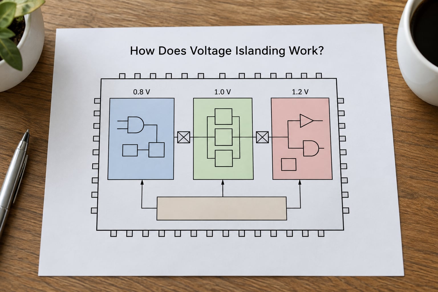
The mechanism is simple to state and fiddly to implement. Each island is a set of hierarchical RTL blocks assigned to a named supply. A supply set groups supplies that belong together, power intent describes which supply feeds which block and under which conditions, and the physical implementation builds a distinct power grid for each one.
A three-domain example makes the topology concrete.
        +-------------------------------------------+
        |            Always-on island  0.6 V         |
        |   reset tree | wake controller | timer     |
        +--------------------+----------------------+
                             |
                    +--------v---------+   (level shifter on every crossing)
                    |  LS / isolation  |
        +-----------+------------------+---------------+
        |                                          |
+-------+------------+              +--------------+-------+
|  Peripherals       |              |  CPU cluster        |
|  UART I2C SPI      |              |  1.2 V              |
|  0.9 V island      |              |                    |
+--------------------+              +--------------------+
   supply: VDD_PERI                   supply: VDD_CORE
Read the drawing as four rules. Blocks inside one island are wired to the same rail and need nothing between them. Anything leaving an island for another voltage passes through a level shifter, in whichever direction the voltage changes. Anything leaving an island that can be powered off passes through an isolation cell, so a collapsed rail does not drive a floating input inside a live block. And anything that clocks into a gated island passes through a clock gate or a clock isolation cell, so no clock reaches a block with no supply.
Clocking and level shifting interact. A level shifter with a high-side rail that is down will not propagate a rising edge, so a clock entering a switchable island at a different voltage needs both a level shifter and gating, in an order the implementation flow decides for you based on the power intent.
What Happens When Signals Cross Voltage Domains?
Every crossing needs a level shifter (also written level converter), a library cell that takes an input signal referenced to one supply and produces an output signal referenced to another. There are three common types, and they are not interchangeable.
| Type | Signal direction | What it needs | What it costs |
|---|---|---|---|
| Low-to-high (L2H) | From a lower rail to a higher rail | The higher rail must be present for the output to swing | Extra delay on the path, always in series |
| High-to-low (H2L) | From a higher rail to a lower rail | Normally a simple buffer, no extra rail | Cheapest and fastest of the three |
| Dual-rail (H2L and L2H combined) | Either direction | Both supplies always available, and sequencing between them | Largest cell, most delay, most verification work |
The L2H case is the one that bites. The receiving input sits at the higher rail’s voltage, and the driving side has to swing far enough to cross that input’s switching threshold, which it cannot do reliably at the lower rail. Timing paths that pass through a shifter are re-analysed at the receiving rail’s characterisation corner, and the delay is path-specific, so a single unconstrained crossing can quietly become the critical path of the whole block.
Two errors show up repeatedly. The first is a crossing that exists in the RTL but has no shifter in the netlist, often because the interface was never declared in the power intent and the tool did not know the two sides ran at different rails. The second is a level shifter placed on a path with no timing exception, so the shift is not visible in the timing report and the path goes unfixed. Neither shows up in RTL simulation with a single supply.
Signals that are not data need the same treatment. Clocks, resets, interrupts and scan enable chains all cross island boundaries, and each one needs its own shifter and gating decision rather than a blanket rule.
How Are Voltage Islands Implemented in RTL and Physical Design?
The flow has seven stages, and the expensive mistakes happen at the first two because everything downstream inherits them.
- Decide the partition. Group blocks by required voltage, which usually means grouping by performance class: cores and accelerators high, uncore and fast fabric mid, peripherals and always-on logic low. Check that each group is physically plausible before you commit, because a partition that has to be spread across the die will not survive placement.
- Assign the voltages. Pick actual numbers against the library’s characterisation corners, and confirm each one leaves enough timing margin for the slowest path in that island. This is the voltage level assignment step in the island-planning literature, and it is where down-volting gets rejected or accepted.
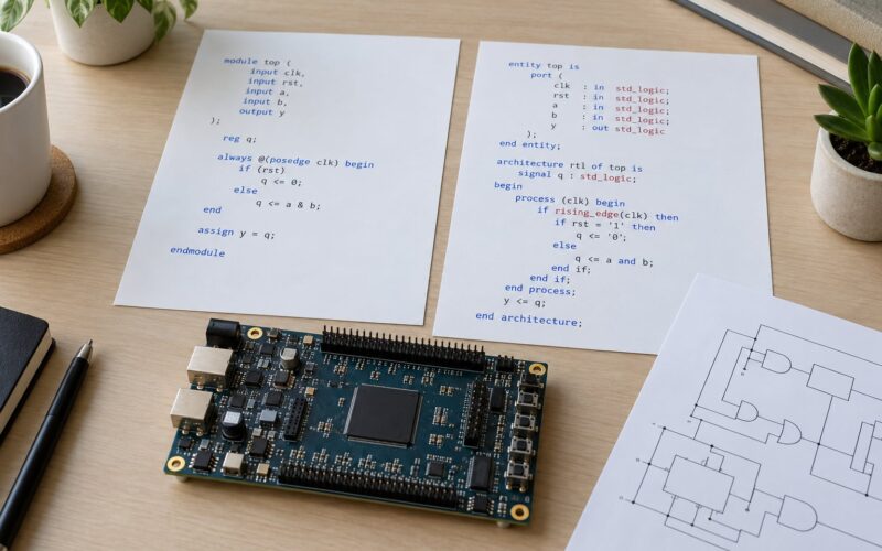
- Write the power intent in UPF. IEEE 1801 is the standard the whole flow reads. Declare supply ports, supply nets, supply sets, the power domains and the elements in each domain. State isolation and level shifter strategies, including which strategy applies to crossings you did not explicitly enumerate.
- Elaborate the RTL with power intent. Synthesis inserts the level shifter, isolation and gating cells described by the UPF, and reports any crossing it could not resolve. Treat that report as a review list, not a warning to dismiss.
- Floorplan for the power delivery network. Give each island its own power stripes or ring, place it near the pads or bumps that feed it, and put well taps and decap where the IR drop budget needs them. Islands placed far from their supply pins spend the power savings on droop.
- Place, route and run CTS. Physical optimisation has to know the rails are different, otherwise it will happily place cells whose high-side rail arrives late, or route a power strap where a signal needed to go.
- Sign off with voltage-aware analysis. IR drop and EM per island, power-aware static timing, low-power equivalence checking, and a power-integrity run that treats each rail separately.
The UPF fragment below shows the shape of the declaration, with two islands at different voltages and a strategy covering crossings.
upf_version 2.1

create_supply_port VDD_CORE
create_supply_port VDD_PERI

create_supply_net VDD_CORE -domain {PD_TOP} -reuse
create_supply_net VDD_PERI -domain {PD_TOP} -reuse

create_supply_set SS_CORE  -function {power VDD_CORE}  -function {ground VSS}
create_supply_set SS_PERI  -function {power VDD_PERI}  -function {ground VSS}

create_power_domain PD_CORE -include {u_core}   -supply {primary SS_CORE}
create_power_domain PD_PERI -include {u_uart u_i2c} -supply {primary SS_PERI}
create_power_domain PD_AON  -include {u_wake} -supply {primary SS_AON}

set_domain_supply_net PD_CORE -primary_power_net VDD_CORE

set_isolation PD_AON -isolation_supply_set SS_AON \
    -isolation_signal wake_ack -isolation_location parent

set_level_shifter SS_CORE -domain PD_CORE -applies_to both \
    -rule low_to_high -location self -input_supply_set SS_CORE \
    -output_supply_set SS_PERI

set_retention PD_PERI -retention_power_net VDD_AON -retention_supply_set SS_AON

add_power_state PD_TOP -state ON \
    -supply {power {SS_CORE  ON 1.20} SS_PERI  ON 0.90} -simstate NORMAL
Two details in that file do most of the work. The default level shifter rule means a crossing nobody thought about still gets a shifter, because the tool applies the strategy to every port at the boundary. And the power state table, which maps a named state to a specific voltage on each supply, is what lets power-aware timing and power-aware simulation reason about a specific mode instead of assuming one rail everywhere.
How Do Voltage Islands Affect Power, Timing, and Area?
The savings are real and the overheads are equally real. Published core-based SoC studies report total power savings in the range of 14 to 28% from partitioning cores onto their own supply voltages, and the IBM SEAS work gives the island-count tradeoff in numbers: three islands achieved a 16.9% power saving at 8.3% area overhead, and four islands reached 17.4% at 7.7% overhead.
That last pair of numbers is the most useful data point in the literature, because it shows diminishing returns. Going from three islands to four bought 0.5 percentage points of power and gave back 0.6 points of area.
| Effect | Direction | Why |
|---|---|---|
| Switching power in a down-volted island | Falls with VDD2 | Less charge per transition |
| Total chip power | Falls, but less than the per-block figure | Only part of the die is down-volted, and overheads add back some |
| Level shifter area | Rises | One shifter per crossing signal, and crossing count grows with island count |
| Path delay on crossings | Rises | Shifter delay is in series with the data path |
| Routing congestion | Rises | Multiple power straps compete for metal |
| IR drop | Redistributes | Each island gets its own budget against its own pads and taps |
| Verification effort | Rises | Every mode is now a combination of domain states |
| Floorplan flexibility | Falls | Islands are tethered to their supply pins |
The total-versus-per-block gap is worth dwelling on. Dropping one peripheral island by 44% sounds like a chip-level 44% and is not: if that island is 20% of the die’s switching power, you have removed about 9% of the total, then subtracted the level shifter, isolation and power grid overhead that came with it.
What Are the Common Voltage Island Design Mistakes?
Every one of these has shown up in real tapeouts, and all of them are caught earlier than you would like.
Missing crossings. A signal crosses between two rails with no level shifter in the netlist. The usual cause is an interface that was never declared in the power intent, so the tool never knew the two sides ran at different voltages. Fix: give the flow a default level shifter strategy and review the unrecognised-crossing report at elaboration.
Isolation in the wrong state. Isolation is declared but the control signal comes from a domain that can be down, so the isolating cell is itself unpowered when it is needed. The signal looks fine in simulation because simulation picks a mode and holds everything up. Fix: state where the isolation supply comes from, and check the supply dependency explicitly.
Missing isolation on gated neighbours. A block is placed in a power domain that will be switched off, and its outputs go straight into a live block. Fix: when a domain is shut down, its boundary signals need isolation regardless of whether the voltage differs.
Incomplete power constraints. A supply is declared without a power state table, so sign-off analysis has no idea which voltage belongs to which mode and quietly reports a single-rail timing result. Fix: name every state and give every supply a voltage in each one.
Unconstrained interfaces. A level shifter sits on a path with no timing exception, so the shift is invisible to static timing and the path stays unfixed. Fix: add false-path or multicycle constraints where a shifter dominates, and constrain the rest properly.
Too many islands. Fragmenting the die into eight or ten rails looks thorough and costs more than it returns. Each island adds cells, straps, pads and a verification state, and the savings flatten out well before that point. Fix: partition by performance class and stop when the next island is not buying meaningful power.
Unbalanced rails. One island carries a large fraction of the die’s total current while drawing from a small share of the pads. Its IR drop eats the savings. Fix: budget current per island and size the pads, stripes, taps and decap to that budget before floorplanning is frozen.
How Do You Verify Voltage Islands Correctly?
Verification is where multi-voltage designs get found out, because the failure modes are combinations of two domains and most of them are invisible in ordinary RTL simulation.
UPF-aware simulation. Run simulation with the power intent attached and power state switching enabled, so a scenario can actually enter a state where a rail collapses. Tests that flip power states and sample the boundary behaviour right after the switch are the ones worth writing; the interesting bugs live in the settling window.
Low-power equivalence checking. Compare the low-power netlist against the RTL under the same power state, with the tool modelling level shifters, isolation and gating. This is what catches a crossing that lost its shifter somewhere between elaboration and the final netlist.
Power-aware static timing analysis. Analyse each mode and each supply voltage separately, with the right characterisation corner per domain. A path that meets timing at 1.2 V tells you nothing about the same path at 0.9 V. Also check that the timing report actually includes the shifter delays, which requires the exceptions to be in place.
Power-aware functional coverage and checks. A rule-based check for anything that crosses a domain boundary without a declared strategy, and for isolation or retention that is declared but never controlled, catches a large share of the remaining bugs before tapeout.
Physical and power-integrity sign-off. IR drop and electromigration per rail, using the actual power grid for that island, plus checks that every island’s taps, stripes and pads are actually connected and that no rail is shorted to another in the layout.
The pattern is consistent across all of them: check the supply combinations, not the logic. The logic is usually fine. What breaks is the corner where one island goes down, or where a rail is lower than the analysis assumed.
Where Voltage Islands Are Heading
Static islands are no longer the leading edge in the places people expect, though they remain the sane default for peripherals and I/O.
For cores, DVFS with an on-die or package regulator has taken over. A regulator lets the same silicon run at several voltages, which a static island by definition cannot do, and it makes the multi-rail physical design problem a control-loop problem instead. A second reason static islands lose ground on the core path: as core voltage falls toward the threshold voltage of the logic, delay stops scaling with VDD, and a core already on the steep part of that curve gets nothing useful from another 100 mV.
On-die voltage regulators also bring their own overhead, which is why designers do not simply replace every island with one. A switched-capacitor or analogue regulator occupies area, has conversion efficiency losses, needs its own stability analysis, and takes time to settle after a frequency change, which shows up directly in wake-up latency.
Chiplets and 3D-IC push the idea further, in a way that is almost the opposite. A chiplet can simply be powered from its own package-level supply, so a whole die gets its own voltage without any island partitioning on it. A 3D-IC face-to-face stack is where islands get more interesting again, because different faces can sit at different rail-to-rail voltages, and through-silicon vias become the level shifters with the tightest constraints of any crossing in the design.
Where the technique is still expanding is ultra-low-voltage design, where the supply approaches or drops below the logic threshold voltage. The physics that makes down-volting attractive is the same physics that makes it dangerous, since the design loses timing margin as it gains power savings, and any leakage variation starts to matter.
Frequently Asked Questions
Are voltage islands the same as power domains?
No. A power domain answers whether a block is connected to its supply or switched off, and is defined by switches, isolation and control. A voltage domain answers at what voltage a block runs, and is defined by which supply feeds it. A block can be in one power domain and one voltage domain at the same time, and the same block boundary can be both. Power domains are about leakage and shut-off; voltage domains are about dynamic power through the VDD squared relationship.
Can a voltage island contain blocks with different supply voltages?
No, not by definition. A voltage island is a set of blocks sharing one supply voltage, so having two different voltages inside it means it is really two islands that happen to be adjacent. What you can have is several islands grouped into one power domain, where they share a switch and a control signal but run at different rails. That grouping is common because it keeps the switching and isolation logic simpler, and the power intent files express the two ideas separately.
Why are level shifters needed between voltage islands?
Because a CMOS input is referenced to its own local supply rail. A signal driven from a 0.9 V island into a block running at 1.2 V has to swing past the receiving input’s switching threshold, which it cannot do reliably. A level shifter restores that margin. It costs delay in series with the data path and area at every crossing, so the low-to-high direction is the expensive one, the high-to-low direction is usually a simple buffer, and dual-rail cells are used when the voltage relationship is not known to be fixed.
How do voltage islands affect timing closure?
They add delay at every crossing through the level shifter, and they force analysis to be done per voltage and per mode rather than once at a single rail. A path that closes at 1.2 V may not close at 0.9 V in the same island, and the shifter itself is characterised at the receiving corner. The practical consequences are more timing runs, tighter constraints on cross-domain interfaces, and a floorplan where island placement is limited by proximity to supply pins rather than by data connectivity.
Does using a lower voltage always reduce total chip power?
No, though it nearly always reduces it. Dynamic power falls with the square of supply voltage within an island, so a 1.2 V to 0.9 V drop removes about 44% of that block’s switching power. But only part of the die is down-volted, and the level shifters, isolation cells, extra power grid and larger power pads all add power and area back. In published core-based SoC studies the chip-level saving lands in the 14 to 28% range, well below the per-block figure.
How can an engineer verify that all voltage-domain crossings are correct?
Run UPF-aware simulation with power state switching so a rail can actually collapse, and write tests that sample boundary signals right after a state change. Then run low-power equivalence checking against the RTL with the same power intent, which catches crossings that lost their shifter in implementation. Power-aware static timing analysis per mode and per voltage confirms the delays, and a rule-based check flags any boundary port with no declared level shifter or isolation strategy.
Key Takeaways
Voltage islands in SoC design pay off because switching power scales with VDD squared, and a peripheral that never needed core speed does not need core voltage. The work is in the boundaries: level shifters, isolation, a distinct power grid and pad set per island, and analysis run per voltage and per mode.
If you are starting a design, do three things first. Group blocks by required voltage, pick the numbers and check each one against its slowest path, and write the power intent with a default level shifter strategy so the crossings nobody remembered still get handled. Partition by performance class and stop when the next island stops buying meaningful power.