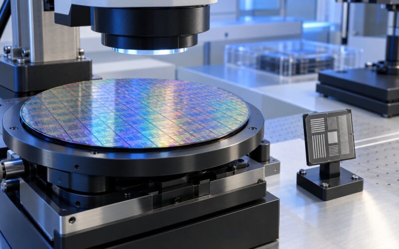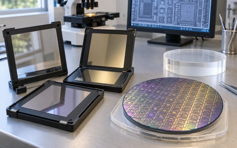
Defect density explained for chip manufacturing comes down to one number: the average number of defects per square centimeter of wafer area, usually written as D0 in defects per square centimeter. That single figure decides what share of each wafer ships as working die, what a good die costs to make, and whether a process node is worth staying on. A D0 of 0.4 def/cm² on a 1 cm² die gives roughly 67 percent die yield. A D0 of 0.1 gives roughly 90 percent.
Most search results muddy this. Generic manufacturing pages define defect density as a percentage of defective parts, which is a different convention entirely and produces completely different numbers. The rest of this guide stays in the semiconductor sense: defects per unit area of wafer, tracked layer by layer, used to model yield.
Table of Contents
- What Is Defect Density in Chip Manufacturing?
- The semiconductor convention, explained
- How Is Defect Density Measured?
- Defect Density Explained: Formulas and Yield Models
- Defect density explained: which yield model to use
- D0 versus DD: the unit trap
- Random Defects, Systematic Defects, and Process Drift
- What Defect Density Means for Die Yield
- How Foundries Control and Reduce Defect Density
- Defect Density Across Advanced Chip Manufacturing
- Common Misunderstandings About Defect Density
- Frequently Asked Questions
- What is the difference between defect density and die yield?
- Is there a single acceptable defect density value for every chip?
- How do semiconductor foundries measure defects on a wafer?
- Does a lower defect density always mean higher final yield?
- Can chip designers reduce defect density directly?
- Why can two wafers with the same average defect density have different yields?
- Conclusion
What Is Defect Density in Chip Manufacturing?
Defect density is the average count of defects per unit of wafer area, expressed in defects per square centimeter (def/cm²). It is a process-health metric, not a product-quality score.
The semiconductor convention, explained
Two definitions of defect density circulate, and mixing them produces nonsense. In general manufacturing QA, defect density is a percentage: defective parts divided by total parts inspected. In semiconductor fabrication, defect density is defects per square centimeter of wafer, and the number is tiny. A process running at 0.1 def/cm² places one defect in every ten square centimeters of wafer, which has no clean equivalent in a parts-defect percentage. Neither convention converts into the other.
Why the area-based convention? Because a fab manufactures area, not parts. When die area shrinks, the same defect population covers a different fraction of every die. Area-normalized density is the only form of the metric that stays comparable across products and process generations.
Defect density matters because it is the gate on manufacturability. Yield sets cost per good die, cost per good die decides whether a node gets volume, and volume decides whether the node gets the next generation. A process that is technically impressive but stuck above 0.4 def/cm² on a small die will lose money long before anyone measures its performance edge.
A concrete case: a foundry ramps a new logic node and holds D0 at 0.4 def/cm². A 0.5 cm² logic die under the Poisson model comes out around 82 percent die yield, so roughly 18 percent of every wafer’s die is scrap that still consumed the full process flow. Push the same line to 0.1 def/cm² and the die yield moves to about 95 percent. That gap is the entire argument for aggressive defect reduction programs, and it is arithmetic rather than opinion.
How Is Defect Density Measured?
Defect density is not counted by hand. It comes out of in-line inspection tools, then gets normalized by the area they scanned.
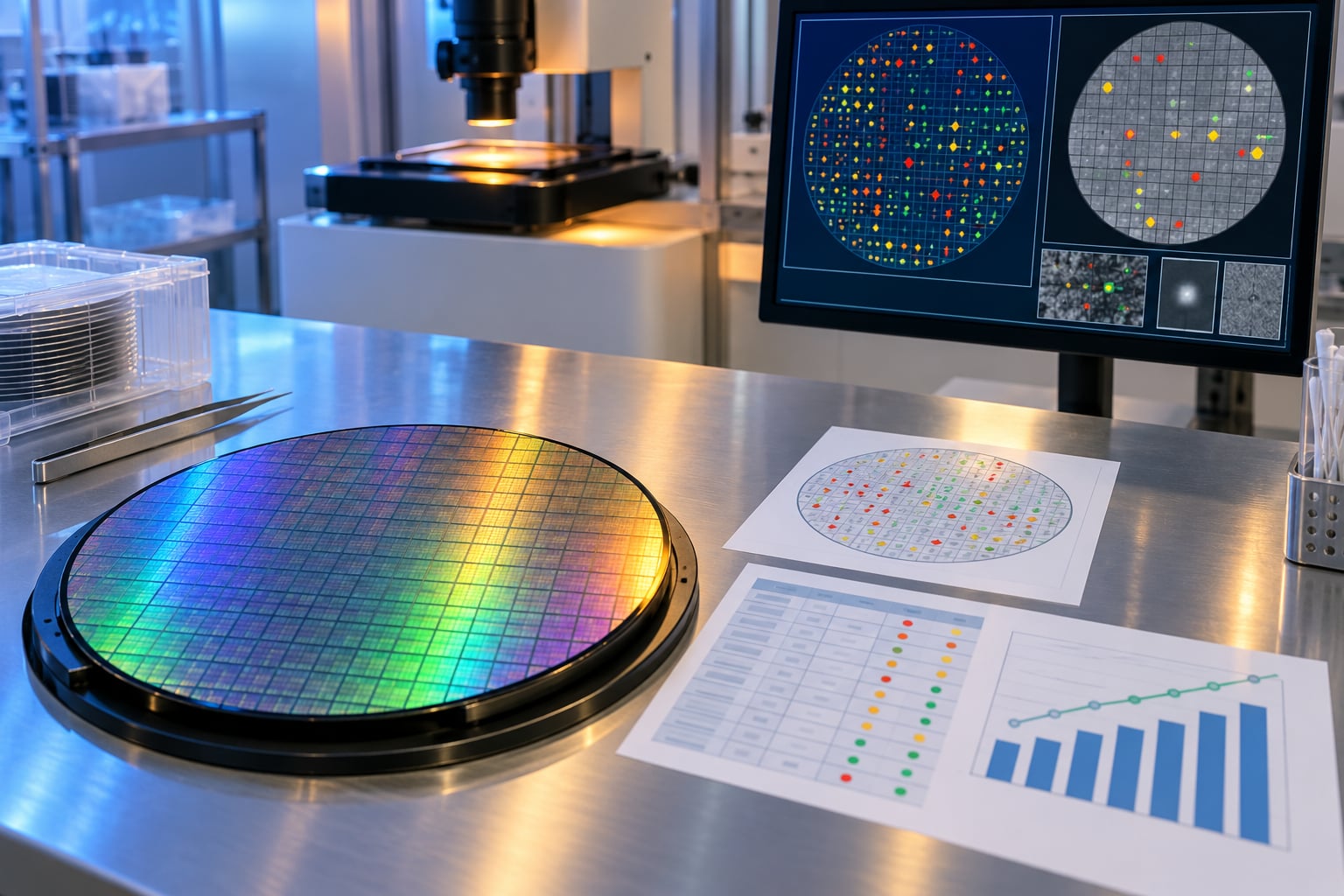
Optical defect inspection systems sweep a moving stage across the wafer after selected process steps, capture hundreds of thousands of images, and flag anything that deviates from the reference. A separate review tool, usually a scanning electron microscope, then classifies flagged sites so engineers can separate particles from film defects, bridges, residues, and pattern-related failures. Classification matters: a site that is a benign speck gets discarded, while a repeating signature across a whole reticle field usually points at a tool or recipe problem.
Three details decide whether the number is trustworthy. First, sampling. Nobody inspects every square centimeter of every wafer at every step, so the count is scaled from a sampled area to the full area, and the sampling plan has to be documented. Second, coverage. Optical inspection catches particles and gross pattern issues; electrical testing catches anything that leaves the die electrically wrong. The two overlap but neither replaces the other. Third, space yield, the fraction of total wafer area covered by good die, which drops below die yield whenever a step adds large exclusion zones around structures.
Substrate-level characterization is a separate discipline. Incoming wafers get measured with etch pit density analysis, X-ray diffraction, atomic force microscopy, photoluminescence mapping, and scanning electron microscopy. For silicon carbide, micropipe density is reported in micropipes per square centimeter, and for SOI and float-zone material, bulk defect counts are specified separately from surface specifications. This is a different question from process defect density: one describes the starting material, the other describes what the process added.
Measurement definitions are not left to chance. SEMI E10 standardizes how yield is reported and measured across the industry, so numbers from different fabs are at least defined the same way.
Defect Density Explained: Formulas and Yield Models
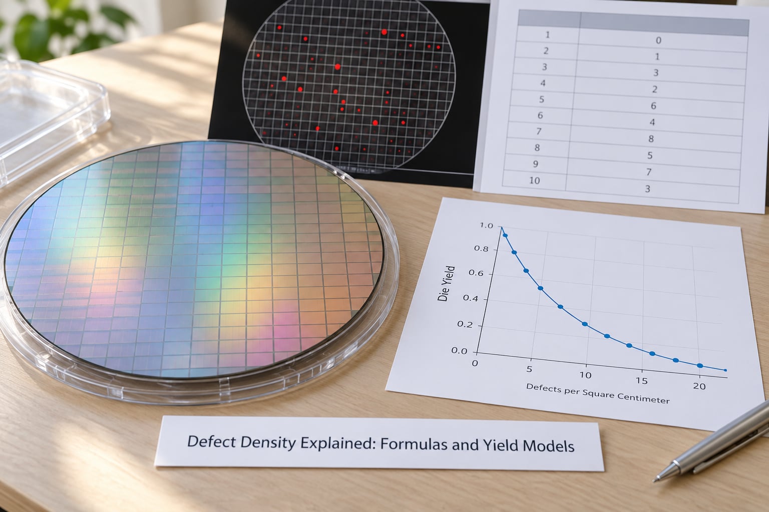
The core relation is the Poisson yield model: die yield equals e raised to the power of minus D0 multiplied by die area, or DY = e^(-D0 × A), where A is die area in square centimeters.
The reasoning is short. If defects are random, each unit of die area has the same independent chance of carrying a defect. The expected defects on one die is λ0 = D0 × A. The probability of zero defects, and therefore of a working die, is the Poisson probability of zero events, e^(-λ0).
Worked example with a 1 cm² die:
- D0 = 0.4 def/cm² gives λ0 = 0.4, and e^-0.4 = 0.670, so about 67 percent die yield.
- D0 = 0.2 def/cm² gives λ0 = 0.2, and e^-0.2 = 0.819, so about 82 percent.
- D0 = 0.1 def/cm² gives λ0 = 0.1, and e^-0.1 = 0.905, so about 90 percent.
- D0 = 0.05 def/cm² gives λ0 = 0.05, and e^-0.05 = 0.951, so about 95 percent.
Note how the curve behaves. The first halving of D0 buys roughly 15 points of yield. The next halving buys about 8. Yield improvements get expensive as the process gets clean, which is why mature nodes sit in a flat region and new nodes spend years climbing out of it.
On a 300 mm wafer with roughly 707 cm² of usable area, a 0.5 cm² die fits about 1,400 times before edge loss. At 82 percent die yield that is roughly 1,150 good die per wafer. At 67 percent it is about 940. Same wafer, same process flow, 210 fewer sellable chips per pass.
Defect density explained: which yield model to use
Poisson is the baseline assumption, and it is wrong in known ways. It assumes defects never cluster and that every defect has the same probability of killing a die. Real processes violate both.
| Model | Core assumption | Where it fits | Known limitation |
|---|---|---|---|
| Poisson | Random, uniformly distributed, non-clustered defects | First-pass line monitoring, mature processes, small die | Predicts unrealistically high yield for large die, where clustering dominates |
| Binomial | A fixed defect count spread over N die sites | Quick mental checks on a single wafer | Assumes the count never varies between wafers |
| Murphy triangular | Defect density rises linearly as process maturity improves | Ramp and yield learning across a node transition | Describes the trend, not a physical distribution |
| Seeds | Distribution of defect densities around a mean | Modeling wafer-to-wafer variation | Needs an assumed density distribution function |
| Bose-Einstein | Defects per square inch per layer, N critical layers | Layer-count-driven analysis of complex processes | Collapses to Poisson when N equals 1 |
| Negative binomial | Clustering, via a cluster parameter alpha | Processes with particle showers or localized hotspots | Alpha is hard to estimate from limited data |
Process engineers rarely pick one. Poisson gives the quick read during monitoring, a clustering model is used when the data shows spatial structure, and the Bose-Einstein form is used when the number of critical layers, rather than raw area, dominates the loss.
D0 versus DD: the unit trap
The second unit in circulation is DD, defects per square inch per layer, and it feeds the Bose-Einstein expression DY = [1 / (1 + DD × A)] raised to the power of N, where A is die area in square inches and N is the number of critical layers.
Conversion runs through 6.4516, since one square centimeter equals 0.155 square inches. So D0 of 0.4 def/cm² equals 2.58 def/in², and divided across 30 critical layers that is DD = 0.086 def/in²/layer. Plugging that back into the Bose-Einstein form with a 1 cm² (0.155 in²) die gives about 67 percent yield, matching the Poisson result almost exactly, which is a useful sanity check whenever two models are cited side by side.
When a news article quotes a defect density number, check which unit it uses before drawing any conclusion from it. The same process reads very differently as 0.4 def/cm² and as 2.58 def/in².
Random Defects, Systematic Defects, and Process Drift
Random defects are isolated particles, film defects, and random opens or shorts. Each one has roughly the same chance of landing anywhere, which is exactly what the Poisson model assumes, and this is where most of a mature process’s defect budget sits.
Systematic defects behave differently. They come from a mask, a recipe, a resist batch, or a chamber that has drifted, and they repeat in a spatial signature: the same die location on every wafer in a lot, an arc on one side of the wafer, a streak along a tool’s travel direction. A systematic defect can be extremely dangerous because it is invisible in a wafer average. Four hundred die all failing the same way on a lot of a thousand wafers is a tiny contribution to the mean defect density, yet it is a total line stop for that design.
Clustering sits between the two. A chamber that sheds particles periodically produces local bursts, so a Poisson calculation understates the loss badly. That is the case the negative binomial cluster parameter exists to describe.
Process drift is the slow version of the same problem. A reticle degrades, a temperature control loop loses margin, a wet bench ages. Each change shows up first as a trend in wafer maps, not as a yield collapse, which is exactly why fabs track spatial signatures and not just the number.
What Defect Density Means for Die Yield
Three different percentages get called yield, and confusing them is the most common source of bad analysis.
Die yield is the fraction of die on a wafer that pass electrical test. Defect yield is the fraction of die that failed specifically because of a detected defect, as opposed to a parametric failure or a design margin problem. Space yield is the fraction of wafer area occupied by good die, which falls below die yield whenever a process step adds dummy fill, alignment marks, or guard structures around working circuits.
Die yield versus defect density under the Poisson model, across common die areas:
| D0 (def/cm²) | 0.5 cm² die | 1 cm² die | 2 cm² die | 5 cm² die |
|---|---|---|---|---|
| 0.05 | 98% | 95% | 90% | 78% |
| 0.1 | 95% | 90% | 82% | 61% |
| 0.2 | 90% | 82% | 67% | 37% |
| 0.4 | 82% | 67% | 45% | 13% |
| 1.0 | 61% | 37% | 14% | 1% |
Read the table down a column and one point becomes obvious: large die are far less forgiving. A 5 cm² die at 0.4 def/cm² lands at 13 percent yield under the random model. Photolithography compute and design-for-manufacturing work exist largely because of that arithmetic, shrinking the sensitive area per function rather than hoping the process gets perfect.
Not all yield loss is defect loss. Edge die around the perimeter of a 300 mm wafer are commonly sacrificed to clamping and handling, and parametric wafer test can exclude die that measure electrically out of spec without any physical defect present. A line reporting 20 percent yield loss from the defect model and 35 percent actual loss has a gap worth investigating, and the gap is usually edge loss, parametric exclusions, or clustering that the model does not capture.
Cost follows directly. Cost per good die is the total wafer processing cost divided by good die, so a process that improves D0 from 0.4 to 0.1 on a small die can cut the scrap portion of cost by more than half without touching a single process step. That is why defect density targets are treated as financial targets in a fab, not just engineering ones.
How Foundries Control and Reduce Defect Density
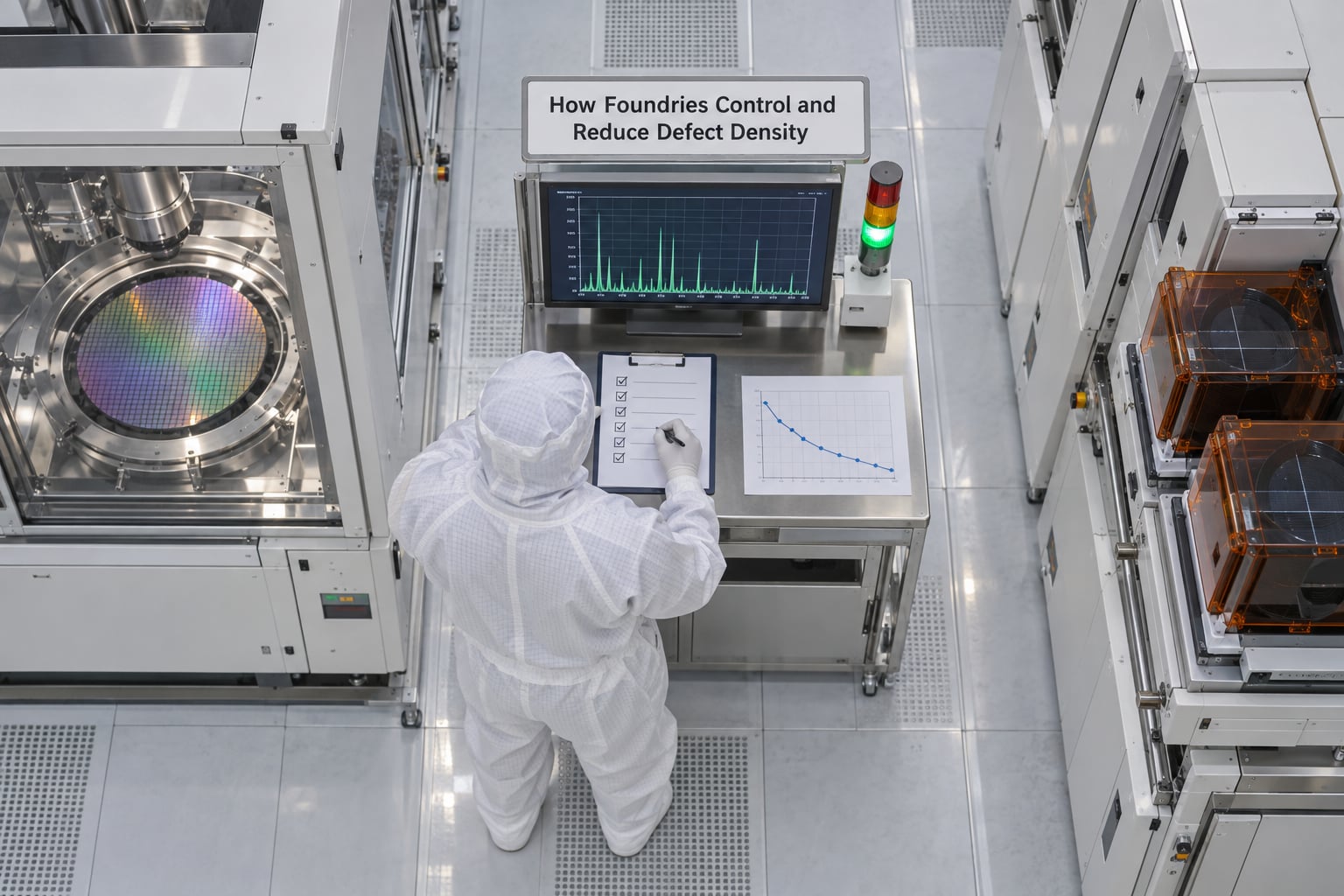
Seven controls do most of the work in a modern fab, and they operate in order of how early they act on a defect. Defect density explained for chip manufacturing always ends up as a control story rather than an equipment story, because no single tool sets the number.
- Cleanroom class and airflow. Particle counts fall as air changes per hour rise. The largest gains come from laminar flow over the most sensitive tools, since a particle landing on an unpatterned wafer usually kills the die.
- Wafer handling and FOUP discipline. Front opening unified pods, automated material handling, and defined pod move times cut human contact, which is a large share of particle events in mature lines.
- Particle monitoring at the tool. Particle counters and wafer-level sensors feed statistical process control charts. An excursion is caught on one tool in one lot rather than at final test across thousands of wafers.
- Preventive maintenance and chamber qualification. Scheduled cleans of deposition and etch chambers, plus routine qualification runs, remove the deposit buildup that generates flakes mid-lot.
- Process window management. Keeping recipes centered in their qualified window, rather than at an edge tuned for speed, reduces sensitivity to small drifts.
- Inline inspection and classification. The detection and disposition loop described earlier, including space yield tracking so exclusion zones do not quietly grow.
- Corrective action loops. Root-cause work on classified defect signatures, closing the loop back into the maintenance and process window controls rather than filing the excursion and moving on.
The last one is where most programs fail. A fab that counts defects but does not close corrective actions has a measurement system, not a control system.
Contamination control extends beyond the cleanroom to the supply chain. Filtered chemicals, traceable specialty gases, and qualified single-wafer processing equipment all feed the same D0 number, and each vendor qualification is judged on the defect contribution it adds rather than on throughput alone.
Defect Density Across Advanced Chip Manufacturing
As nodes shrink, the process gets longer. A leading-edge logic flow runs on the order of a thousand steps, and a meaningful fraction of them are critical in the sense that a defect at that step kills the die. More layers means more opportunities, and each additional critical layer multiplies survival probability, which is exactly what the exponent N in the Bose-Einstein model represents.
EUV lithography added a layer count nobody asked for. It removed the multi-patterning step chains that used to dominate both cost and defect adders, but a single EUV exposure has tight volume and a narrower process window, so marginal defects per layer are higher and the yield learning curve is more sensitive to dose and focus control. Fewer steps at higher per-step difficulty still wins on total defect add, but the win is measured, not assumed.
Industry process targets are set in this space. Intel has publicly framed its 18A-class process around a D0 target below 0.40 def/cm², and SemiWiki forum discussion of Intel 14A framed the goal as a push toward 0.1 to 0.2 def/cm². Those numbers only make sense next to a die area and a layer count.
One caution for readers of process news: node size alone does not determine defect density. A mature 28 nm node with clean chambers and disciplined handling can beat an immature 7 nm node with none of that. What determines D0 is process maturity and control, not the number on the marketing slide.
Common Misunderstandings About Defect Density
Defects per die versus defects per area. A quoted D0 is a wafer area density. To get expected defects per die, multiply by die area. The mistake goes both ways, and it is why a 0.4 def/cm² figure is sometimes read as catastrophic and sometimes as excellent.
Inspection counts versus electrical failures. An optical inspection count is a detection, not a failure. Some flagged sites are electrically harmless, and some electrical failures never produced a visible signature. The two are correlated, not identical, and the ratio between them shifts with defect type.
Lower D0 does not guarantee a specific yield. Poisson assumes randomness. Systematic failures, clustering, edge loss, and parametric exclusions all break that assumption, which is why actual yield can land well below the model at a perfectly respectable D0.
The ppm question. Parts per million is the wrong unit for a fab process. A mature semiconductor line works at defect densities of tenths of a defect per square centimeter, and the customer-facing reliability measure that is quoted in ppm is a different quantity entirely, drawn from final test and field returns. If a source gives you a defect rate in ppm without saying whether it means inspection defects, test failures, or field returns, the number cannot be interpreted.
Inspection coverage is silent. Two fabs can both report 0.2 def/cm² where one inspected 100 percent of critical layers and the other sampled 20 percent. Coverage belongs next to the number, every time.
One wafer average describes nothing. A single average across a wafer, a lot, or a year hides every tool signature that matters. The map is where the diagnosis lives.
Frequently Asked Questions
What is the difference between defect density and die yield?
Defect density is an input, die yield is an output. Defect density counts defects per square centimeter of wafer area. Die yield is the fraction of die on a wafer that pass electrical test. Under the Poisson model the two connect through die yield = e^(-D0 x A), where A is die area in square centimeters. Defect density describes the process; die yield describes the product.
Is there a single acceptable defect density value for every chip?
No. Acceptable defect density depends on die area, layer count, and what the product is worth. A 0.4 def/cm2 process gives about 82 percent yield on a 0.5 cm2 die but only 13 percent on a 5 cm2 die. A large, expensive die tolerates less density than a small one because the same areal density eats a much larger share of the die. Targets are always set per product.
How do semiconductor foundries measure defects on a wafer?
Optical defect inspection tools scan a moving stage across the wafer after selected process steps, capture images, and flag sites that deviate from a reference. A review tool, usually a scanning electron microscope, classifies those sites as particles, film defects, bridges, residues, or pattern-related failures. The sampled count is scaled to full wafer area, and sampling coverage is documented with the result. SEMI E10 standardizes how yield itself is measured and reported.
Does a lower defect density always mean higher final yield?
Not always. Poisson assumes defects are random and non-clustered, and real processes break that assumption. Systematic failures, particle clustering, edge die loss, and parametric test exclusions all reduce yield independently of the areal defect density. If a process meets its D0 target but yield still trails the model, the gap is usually clustering or a systematic signature rather than a defect-density measurement problem.
Can chip designers reduce defect density directly?
Not directly. Defect density is a property of the process, and engineers cannot set it from a design file. What designers do control is sensitivity to it: smaller sensitive area per function, design-for-manufacturing rules, redundant structures that tolerate one defect, and matching the layout to the process. Those choices change how much of the process defect budget actually lands on a working die, which is why yield engineers sit in on design reviews.
Why can two wafers with the same average defect density have different yields?
The average is a summary, and it discards the spatial map. One wafer may have defects scattered evenly while another has a dense cluster in a single quadrant from a chamber that shed particles. Both report the same areal average, but the clustered wafer loses whole die while the even wafer loses isolated ones. Systematic signatures matter for the same reason: four hundred die failing identically across a lot barely move the mean and still stop the line.
Conclusion
Start with a baseline, not a target. Build a normalized, inspection-backed D0 figure for a known product, document the sampling coverage it came from, and map it by wafer, lot, tool, and process step. Then track the trend rather than the number. A falling D0 with a rising systematic signature means the average is improving while the line gets less predictable, and only the map tells you which one you are looking at.
That is what defect density explained for chip manufacturing should leave you with: a defensible baseline, a map, and a trend worth acting on.