How chips are tested after manufacturing comes down to two main stages. Wafer sort, also called wafer probe test, happens while the die is still attached to the wafer. Final test happens after the chip has been cut, packaged and assembled. Together they separate good dies from defective ones so nothing faulty moves down the line.
The point is economic as much as technical. Packaging, board assembly and shipment all cost real money, and a defect found early is cheap to discard. It also feeds process engineers the yield data they need to raise the next lot.
Test lives at the back end of the flow, after wafer fabrication and assembly. Everything before it is front-end work; everything after it is back-end handling, and final test is the last checkpoint before a part leaves the building.
Table of Contents
- What Happens When a Chip Is Tested After Manufacturing?
- The Main Stages of Semiconductor Testing
- How Electrical Test Finds a Defective Chip
- How Chips Are Tested
- How chips are tested after manufacturing, step by step
- What test engineers actually write
- What Is Wafer Probe and Why Does It Happen Before Packaging?
- What Happens During Final Electrical Test?
- What Is Burn-In Testing?
- How Reliability Qualification Differs From Production Test
- What Test Equipment and Test Structures Are Used?
- How Yield Data Is Collected and Used
- Inspection and Electrical Testing: How They Work Together
- Frequently Asked Questions
- Are all chips tested after manufacturing?
- How long does it take to test a chip?
- What is the difference between wafer probe and final test?
- What causes a chip to fail testing?
- Can software replace hardware testing during manufacturing?
- Key Takeaways
What Happens When a Chip Is Tested After Manufacturing?
When a chip is tested after manufacturing, an automated tester drives known voltages, currents and signal patterns into the device, measures the electrical response, and compares every reading against limits taken from the datasheet.
Each part then gets one of two outcomes: it passes and continues, or it fails and goes into a reject or downgrade stream. What makes the step worthwhile is where it sits. A die that fails on the wafer has cost a wafer and a probe card touch. The same die found after packaging has already cost a package, assembly labour, board real estate and shipping.
It helps to keep four activities apart, because they get mixed up constantly:
- Electrical test applies electrical stimuli and measures responses. This is what this whole article is about.
- Inspection looks at the part with optics or X-rays to catch physical damage that electrical test may not reveal.
- Process control samples structures on the wafer during fabrication, long before a full test program exists.
- Reliability qualification stresses a small sample of parts over months to prove the design lasts, rather than checking every part today.
Those last two answer a different question. Test asks whether this part works now. Qualification asks whether this part family will still work in five years.
The Main Stages of Semiconductor Testing
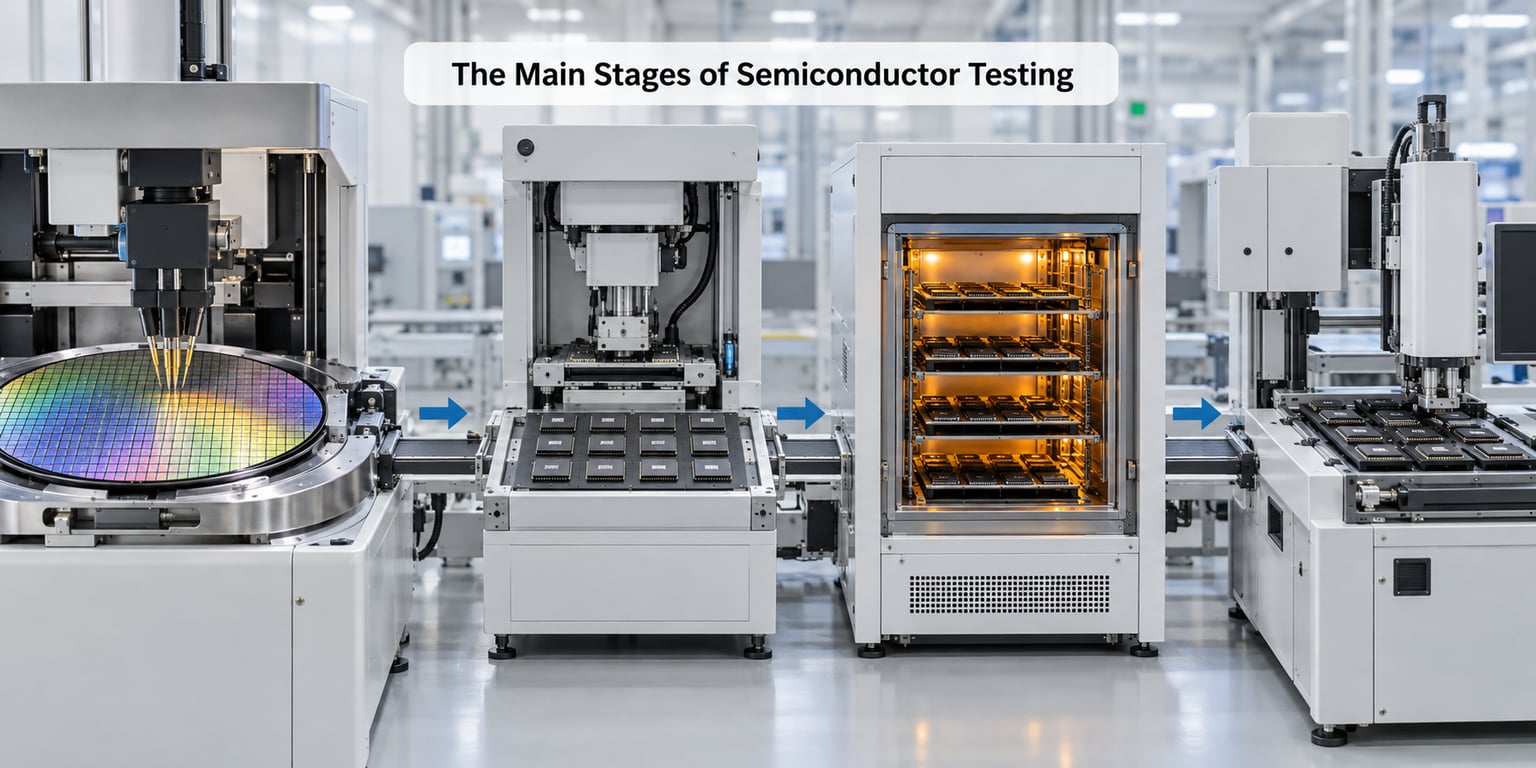
Here is the sequence most integrated circuits follow, from wafer to outgoing shipment.
- Electrical parameter monitoring (EPM) — inline structures on the wafer are measured during fabrication to catch process drift early, before any device is fully built.
- Wafer burn-in — for memory and some logic parts, the wafer is held at elevated temperature and voltage so weak cells fail while repair is still possible.
- Wafer sort (probe test) — a probe card touches the pads of every die in turn, and each die is measured and marked pass or fail.
- Repair — failing bits are swapped for spare redundancy cells, turning a partially good memory die into a shippable one.
- Dicing and packaging — good dies are cut apart and mounted in a package with bond wires, solder balls or hybrid bonding.
- Final test — packaged parts are loaded into handlers, connected through a socket, and retested across voltage and temperature corners.
- Visual test, marking and sort — packages are inspected, laser marked for traceability, and graded into bins such as speed grades before tray pack.
Some flows insert a system-level test after step six, where the chip runs in a real board or module rather than a socket. Burn-in for high-reliability parts happens between packaging and final test or after it, depending on the device.
How Electrical Test Finds a Defective Chip
Electrical tests are grouped into a handful of families, and each one narrows down a different class of failure.
Continuity and leakage tests check that pins connect where the design expects and do not connect where it should not. A connection that never closes is an open. Two nodes tied together by unintended metal or a bridged solder ball is a short. Both show up as an out-of-limit resistance reading.
DC parametric tests sweep voltage and measure current. This catches a die drawing far more current than its datasheet allows, often the earliest sign of a shorted gate or a leaky junction.
AC parametric tests apply a signal and measure timing, rise and fall time, and output drive. A circuit that is built correctly but runs too slowly fails here and nowhere else, which is why speed grading comes from AC results.
Functional and pattern tests load a test pattern into internal registers or memory and check the response. A stuck-at fault, where a bit never changes from zero or one, shows up immediately as a pattern mismatch.
Structural tests walk the internal scan chain and read out internal nodes, so a fault buried in the middle of a block can be isolated without a scanner costing more than the fab that made the die.
Put together, those tests turn a functioning-looking part into a pass or fail decision backed by numbers.
How Chips Are Tested
How chips are tested after manufacturing, step by step
The mechanics look different at each stage, but the loop is the same every time.
- Preparation and setup. The device under test, the load board or probe card, and the test program are matched. Limits come straight from the datasheet, adjusted for the temperature corner being run.
- Physical connection. A probe card touches die pads on the wafer, or a handler places a package into a socket on a load board. Contact resistance matters, so probe pins are cleaned and sockets replaced on a schedule.
- Vector application. The automated test equipment drives pins with programmed patterns and holds each device in a defined electrical state.
- Measurement and comparison. Every reading is captured, compared to its limit, and logged with a pass or fail bit.
- Diagnosis and retest. Parts that fail are re-run to separate a real failure from a contact glitch, then binned. Repeated failures at the same address usually mean a layout or process problem rather than a bad part.
- Data capture. Test time, yield, bin distribution and failure signatures are written to a database and reviewed by yield engineers.
What test engineers actually write
Most of the job is the test program, not the hardware. A test engineer takes the datasheet, turns each row into a measurement with a limit, writes the patterns that exercise the logic, and decides which tests are worth their cost in cycle time.
The judgement is in the tradeoffs. A longer program finds more defects but consumes tester hours that are already the constraint. Test insertion also means correlation work, checking that two different testers agree on the same part, which is why test engineers are a distinct role in most organisations. It is one people in the industry talk about as a career of its own, separate from design verification.
What Is Wafer Probe and Why Does It Happen Before Packaging?
Wafer probe tests each die while it is still bonded to the wafer, and it exists for one dominant reason: cost.
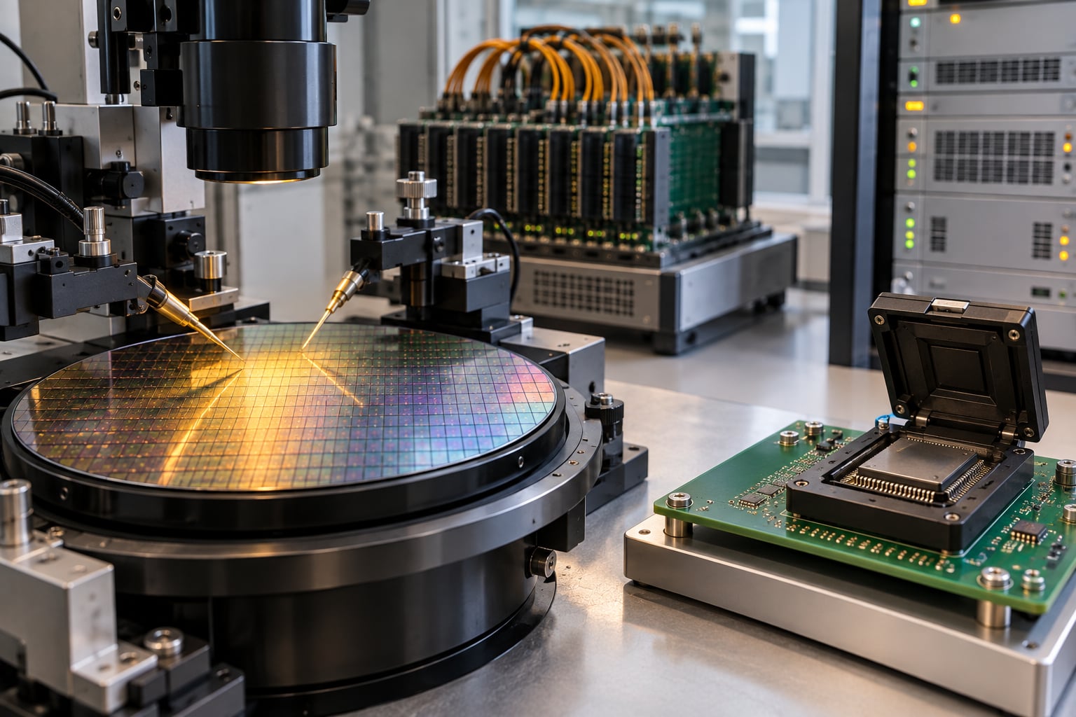
A probe card is a ceramic or glass plate carrying hundreds of fine probe pins, one per pad or group of pads on a die. The wafer prober holds the wafer at a set temperature, steps from die to die across a reticle field, and lowers the card so the pins land on each die’s bond pads in turn. The tester runs the same test program it will later run in final test, and records a result per coordinate.
Three details matter to engineers.
- Known good die. The output is a wafer map: which coordinates passed, which failed, and how. Assembly planners use the count of known good dies to schedule capacity, because a wafer with poor yield still has to be packaged die by die.
- Probe marks. Those pin contacts leave marks on the pads. Too aggressive a probe leaves damage that shows up as an intermittent open weeks later, so probe force and tip material are tuned constantly.
- Wafer sort is not final test. Wafer probe confirms the silicon works. It cannot confirm the packaging, the bond wires or the solder joints, because none of those exist yet.
What Happens During Final Electrical Test?
Final test runs after packaging, and it is the last chance to catch a part before a customer sees it.
A test handler picks parts from a tray, places them into sockets on a load board, closes the lid to make contact, and signals the tester. The automated test equipment runs electrical, functional and parametric tests, often at more than one temperature corner: cold, room and hot, since a device that passes at 25 degrees can fail the limits at the extremes.
Parts are then graded. A memory part that meets the fastest timing bin gets marked with that grade; a part that passes at a lower speed grade still ships in a different bin at a different price point. Visual inspection looks for package cracks, marking problems and solder issues, and a laser mark adds the lot code so a failure can be traced back later.
Final test is also where defects introduced by packaging get found: a missing or lifted bond wire, a solder ball that failed to wet properly, or a substrate delamination that changes the thermal behaviour. None of those existed at wafer probe.
| Aspect | Wafer sort (probe test) | Final test (package test) |
|---|---|---|
| When it runs | After wafer fabrication, before dicing | After dicing and packaging |
| What is tested | Die still attached to the wafer | Finished package |
| Contact method | Probe card pins on die pads | Test socket on a load board |
| Equipment | Wafer prober plus ATE | Test handler plus ATE |
| Typical tests | DC, AC, functional, continuity | DC, AC, functional, speed, parametric |
| Main output | Wafer map and known good die count | Pass or fail, grade, bin, serial traceability |
| Catches | Silicon defects, opens, shorts, leakage | Everything wafer sort found, plus packaging defects |
What Is Burn-In Testing?
Burn-in stresses a part at elevated temperature and voltage for hours or days to surface latent defects that pass a normal test but fail soon after shipping.
The reason is the bathtub curve. Early in a device’s life, the failure rate is high because of manufacturing defects. That infant-mortality period drops sharply after screening, then flattens into a long random-failure phase, and finally climbs again at end of life. Burn-in exists to burn through that first section while the part is still on the test floor, where scrapping it is cheap.
Typical conditions are elevated temperature, often above the rated maximum, combined with higher-than-normal supply voltage. Memory makers do wafer-level burn-in before dicing so failing cells can be replaced with redundancy cells. Logic parts more often burn in after packaging, either in a dedicated board or, in test-during-burn-in setups, while electrical measurements are taken in the same stress environment.
Not everything burns in. A consumer microcontroller that ships in a remote control does not need days of stress. A part destined for a satellite or a surgical device does. So do most parts sold as automotive-grade, which is why test plans are set by the application rather than by the device alone.
How Reliability Qualification Differs From Production Test
Production test checks every part, briefly, against known limits. Reliability qualification checks a small sample, slowly, against failure over time.
Qualification runs to standards such as JEDEC, and the sample is drawn from production material so it reflects real process variation. Typical stress tests include temperature cycling between hot and cold extremes, humidity plus bias such as HAST, high-temperature operating life, and mechanical stress like vibration and drop. Life testing runs parts well past their expected service life to extrapolate the wear-out point.
Application-specific validation comes on top of the standard set, simulating the actual duty cycle: a part in a car sees a different power profile than one in a server.
What qualification does not do is screen parts. It produces statistical evidence that a design and process combination is sound. It never inspects the individual device on your desk. Both layers are required: qualification protects the design, production test protects the customer.
What Test Equipment and Test Structures Are Used?
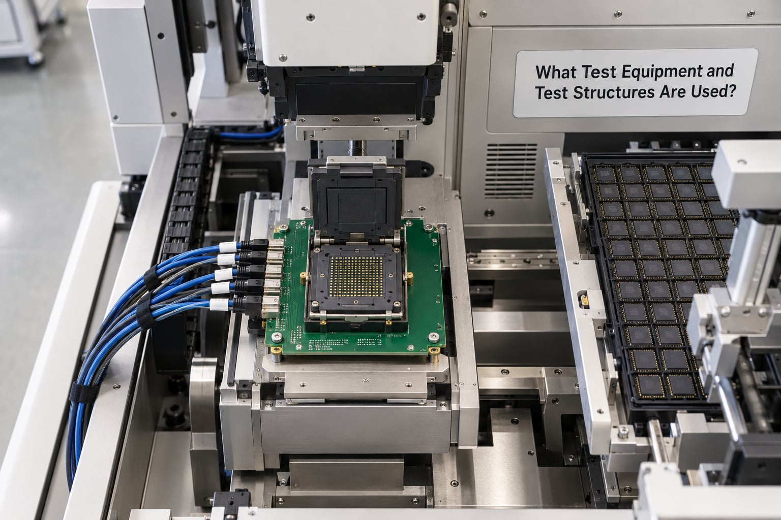
Each tool in the flow has one job, and they only work as a set.
- Automated test equipment (ATE) is the measurement platform itself: pin electronics that drive and sense, pattern generators, power supplies and timing measurement hardware, all running the test program.
- Probe stations and wafer probers present each die to the probe card and control temperature and stepping.
- Probe cards carry the fine pins, and designing one for a new device is a real engineering task in itself.
- Load boards and test sockets route tester channels to package pins at final test.
- Test handlers load parts into sockets, move them between temperatures and sort them into bins or trays at the end.
- Burn-in boards hold many packages under stress, often with sockets designed for repeated thermal cycling.
- Scan structures, boundary scan and JTAG are built into the chip at design time so a tester can reach internal logic. Most digital designs include them specifically to make test affordable.
- Built-in self-test (BIST) runs internal test routines on the chip itself, which lets memory and large logic blocks verify themselves at boot.
Test structures are the reason advanced nodes need more test insertions rather than less. Logic built at smaller nodes relies more on internal redundancy, and more of that redundancy has to be exercised and verified before anyone can trust the yield number.
How Yield Data Is Collected and Used
Every test run produces data, and the value is in reading it rather than staring at pass rates.
First-pass yield is the share of parts passing on the first attempt. Retest yield measures what passes after a rerun. A healthy line keeps those two close; a gap means contact or socket problems, not a process shift.
Defect maps plot failures by wafer coordinate. A cluster of failures at the wafer edge usually points to an edge exclusion or a chucking problem. Failures following a spiral or a specific tool signature point at process equipment instead. Bin maps do the same thing by grade, which is how a slow speed grade tied to one region of the wafer gets spotted.
Signature analysis groups failures that fail the same way, since a recurring pattern means a repeatable defect rather than random noise.
Engineers then act on what they see: tighten a process limit, change a mask, adjust probe force, rework a fixture, or flag a supplier. Test data is one of the main ways a yield problem in the fab gets discovered before it reaches the customer.
Inspection and Electrical Testing: How They Work Together
Inspection and electrical test catch different things, and the gap between them is where defective parts escape to the field.
Optical inspection looks for surface defects, cracks, contamination and marking errors. X-ray inspection sees inside the package, revealing voids under solder balls, delamination, broken bond wires and misplaced components that a surface view cannot reach.
Process monitoring structures built alongside the product on the wafer are measured during fabrication. They are not the product, so they can be sacrificial and instrumented more heavily than real circuits.
Electrical test confirms behaviour. It will pass a part with a cosmetic defect, and it can miss a latent packaging weakness that only matters after thermal cycling. Combining the two narrows the escape rate, which is the number quality engineers actually watch.
When a part does escape, failure analysis takes over using X-ray, SEM, TEM, AFM, time-domain reflectometry and laser voltage probing to find where the failure actually lives.
Frequently Asked Questions
Are all chips tested after manufacturing?
Most semiconductor products undergo at least one form of electrical testing, but coverage differs by product. High-volume digital, analog, memory, RF and safety-critical devices commonly use structured test programs, while very low-cost parts may get sample or reduced coverage. Even then, something is always measured, because shipping untested parts means field failures land on the customer instead of on a yield report.
How long does it take to test a chip?
It depends on the device, package, test method and number of measured conditions. A simple die can be probed in seconds during wafer sort. Complex processors, memory devices and RF parts can take minutes per part at final test, plus hours or days if burn-in is required. Step time multiplied by the parallel site count of the tester determines the real throughput, which is why cycle time is one of the hardest constraints in test.
What is the difference between wafer probe and final test?
Wafer probe tests a die while it is still attached to the wafer, using a probe card to contact its pads. Final test happens after singulation, assembly and packaging, when a handler and test board connect through a socket. Wafer probe screens the silicon and produces a wafer map of known good dies. Final test re-checks the same electrical behaviour and catches defects that packaging introduced.
What causes a chip to fail testing?
A failure may present as an open, short, leakage, timing error, incorrect voltage or a malfunctioning circuit. The underlying cause can be a manufacturing defect in the wafer, a packaging problem such as a missing bond wire or cracked substrate, damage from handling, a marginal design pushed outside its limits at temperature, or a bad contact on the probe card or socket. Re-running the part and mapping the failures usually tells you which one it is.
Can software replace hardware testing during manufacturing?
No. Built-in self-test and JTAG let a chip test some of its own internals, which cuts hardware test cost, but they still need electrical stimulus and measurement from a tester. Software cannot create known good die, detect a cracked package, or prove the part works across temperature. Built-in self-test is a way of making hardware testing cheaper and faster, not of replacing it.
Key Takeaways
Wafer sort screens the silicon while it is still cheap to discard. Final test re-checks the packaged part and catches what packaging broke. Burn-in filters out latent defects that would otherwise fail in a customer’s hands, and qualification proves the design lasts without inspecting every part.
Start by writing down four things: what the part must do per the datasheet, which defects matter most, what quality level the application demands, and what the test is allowed to cost per die. Those four answers decide the flow. A test plan built without them either wastes tester hours catching defects nobody cares about, or ships parts that fail in the field.