Here is the short answer: transistors shrink because lithography keeps printing smaller features, and for decades each generation cut key dimensions by roughly 0.7x while doubling the number of transistors on the same area of silicon. Scaling is slowing down because the voltage needed to switch a transistor cleanly, the heat it produces, the resistance of the wires connecting it and the cost of printing it have all climbed faster than density. Understanding how transistors shrink and why scaling is slowing down matters because every forecast about computing after 2026 rests on which of those four constraints binds first.
The single biggest misconception is that a node name is a measurement. A process called 2 nm tells you almost nothing about the length of a gate or the pitch of a metal line. It is a generation label, and generations stopped corresponding to uniform physical shrinkage a long time ago.
Table of Contents
- What does it mean for transistors to shrink?
- How did transistors shrink from micrometers to nanometers?
- How does Moore’s law describe transistor scaling?
- Why is scaling slowing down at smaller nodes?
- How transistors shrink, and why scaling is slowing down, barrier by barrier
- Why do transistors use FinFET and gate-all-around structures?
- What are the main physical limits on transistor scaling?
- How do chipmakers keep improving chips without simple shrinking?
- What does the slowing of Moore scaling mean for the semiconductor industry?
- A cross-sectional view of modern transistor scaling
- Where atomic scale changes transistor behavior
- Frequently Asked Questions
- Is Moore’s law the same as transistor scaling?
- What does a 3 nm or 2 nm process node actually mean?
- Why can’t transistors keep getting smaller indefinitely?
- Are transistors physically shrinking as quickly as process-node names suggest?
- Does advanced packaging mean chips are not getting smaller?
- Conclusion
What does it mean for transistors to shrink?
A transistor shrinks in several different ways at once, and those ways no longer move together. The gate that controls the channel gets narrower, the insulating layer under it gets thinner, the source and drain get closer, and the wires that carry signals between transistors get tighter in pitch. Density, the number of transistors per square millimetre, is the metric that matters commercially because cost and performance are both quoted per unit of density.
| Term | What it actually describes |
|---|---|
| Process node name | A generation label such as 7 nm or 3 nm, used for marketing and for matching designs across fabs |
| Gate length | The physical length of the gate electrode that controls the channel, a real dimension in nanometres |
| Contacted poly pitch | The repeating horizontal distance between gate contacts; the closest thing to a headline geometric number |
| Transistor density | Transistors per square millimetre, the number Moore originally observed doubling |
| Performance | Instructions per second or operations per second, which depends on frequency, width, power and software, not just density |
Two chips labelled with different nodes can have nearly identical gate lengths and very different densities. Density can also be bought with a larger die rather than a smaller transistor, which is one reason a modern flagship chip contains far more transistors than a laptop chip of ten years ago.
How did transistors shrink from micrometers to nanometers?
The history is a long sequence of changes in structure, materials and printing, not one continuous squeeze.
| Era | Key change | Printing |
|---|---|---|
| 1970s | Planar single-gate transistors, metal interconnect, micron-scale | Optical lithography with g-line and i-line |
| 1980s to 1990s | Sub-micron planar scaling, polysilicon gates, aluminium wiring giving way to copper | Deep ultraviolet stepper lithography with optical correction |
| 2000s | Strained silicon to improve carrier mobility, high-k dielectric with a metal gate to cut leakage | DUV immersion lithography |
| 2011 onward | FinFET, a fin-shaped channel with gates on three sides | DUV immersion, later EUV |
| Mid-2010s onward | EUV lithography at 13.5 nm wavelength, then gate-all-around nanosheets with gates on four sides | EUV, now high-NA EUV |
| Next | Stacked complementary devices, backside power delivery, 3D logic stacking | EUV with multiple patterning |
Planar scaling ran out of road because a single gate could not hold a longer channel in check once the channel got very short. The 3D answer, first shipping commercially in 2011, turned the channel into a thin fin so a gate could approach it from three directions. EUV mattered for a different reason: 13.5 nm light is short enough that a single exposure can print features that would previously have needed several patterning steps, which removes cost and mask complexity.
How does Moore’s law describe transistor scaling?
Moore’s law is an observation about density, first published in 1965 and revised in 1975 from doubling every year to doubling roughly every two years. What doubles is the number of components that fit on an integrated circuit, not speed, not software quality and not battery life. In practice, each generation also multiplied individual transistor performance, which is why density gains translated into usable speed for most of the industry’s history.
| Year | Representative part | Transistor count |
|---|---|---|
| 1959 | First commercial integrated planar transistor | 1 |
| 1971 | First commercial microprocessor | About 2,300 |
| 1978 | Early 16-bit microprocessor | About 29,000 |
| 1993 | First Pentium | About 3.1 million |
| 2006 | Last of the big Itanium generation | About 291 million |
| 2015 | Server processor, 28 nm | About 7 billion |
| 2023 to 2026 | Leading-edge desktop processor | Roughly 19 to 30 billion |
Two other trends drifted away from density. Clock frequency stopped climbing around 2005 and has barely moved since, so speed now comes from more cores, wider execution and accelerators. Cost per transistor flattened out too: the price of one transistor stopped falling at a steady rate once transistors stopped costing far less to make than to connect, power and cool.
Why is scaling slowing down at smaller nodes?
Short-channel effects and the voltage floor are the core reason. As the channel gets shorter, the drain’s electric field reaches through the channel and weakens the gate’s ability to switch the device, a leakier and harder-to-control transistor. Holding that leakage down needs a higher threshold voltage, which means more energy per switch, and voltage cannot rise indefinitely because that would destroy the insulating oxide and destroy reliability along with it. Everything else on the list follows from that squeeze or from the fact that wires, heat and capital do not shrink at 0.7x.
How transistors shrink, and why scaling is slowing down, barrier by barrier
1. Voltage and the noise floor. Signal swings have shrunk only modestly across many generations. Once the usable voltage range stops falling with the transistor, you cannot keep shrinking the device and still read its state reliably, which is why the industry talks about a voltage floor rather than an atomic wall.
2. Leakage current at nanoscale dimensions. A transistor that is supposed to be off still passes current, and standing leakage burns power even when nothing is happening. Power density rises with every added core, and cooling a data-centre rack becomes the constraint that decides how many cores you can ship at all. Designers regularly describe dark silicon, the situation where thermal limits mean some transistors on a die must stay unpowered because switching them all on at full frequency would exceed the cooling budget.
3. Interconnect and RC delay. Design engineers point out that wire delay now dominates logic delay at advanced nodes. Metal wires are getting narrower and longer in terms of resistance per unit length, while their capacitance does not fall proportionally, so the resistance-capacitance product that sets signal delay grows as wires shrink. Adding copper-cobalt or ruthenium liners, and more layers of wiring, costs area and money that could have gone to more transistors. A chip can have more transistors and still take longer to respond.
4. Atomic-scale variation. When a channel is only a few tens of atoms long, one missing or extra atom changes behaviour measurably. A 10% difference in dopant count between neighbouring devices produces visible speed and leakage spread, so designers must reserve margin for the worst device on the die rather than the average one.
5. Lithography complexity and throughput. Each new node needs tighter process control, more mask steps and more exposure passes, and the new high-NA EUV machines in production lines use 0.55 numerical aperture rather than 0.33. Resolution is the headline number, but throughput is the practical problem: the tool writes a smaller pattern, so holding wafers per hour costs more exposure time, and a lower defect density is harder to reach on a smaller print.
6. Mask, yield and design cost. A leading-edge mask set is far more expensive than it was two generations ago, and a defect that used to hit one transistor now ruins a critical structure. Verification alone on a billion-transistor design takes engineer-years, and a tape-out mistake is a strategic failure rather than a fixed cost.
7. Heat removal. Joule heating does not go away when a transistor gets smaller; the energy per switching event at a given voltage stays roughly the same. Since more transistors per area means more heat per area, cooling has to keep pace, and liquid cooling plus advanced packaging has become part of the road map rather than a facility decision.
Why do transistors use FinFET and gate-all-around structures?
Wrapping the channel in a gate gives better electrostatic control. A gate on three sides, or four, holds the channel’s carriers far more firmly than a single gate on one side, so the device keeps a useful on-to-off ratio at a shorter channel length. That is the whole reason for the move to 3D channels.
| Structure | Gate contact | Control at short channel | What it costs you |
|---|---|---|---|
| Planar | One side | Weakest; leakage rises quickly | Simple process, but stopped scaling around 20 nm |
| FinFET | Three sides of a fin | Good; widely used for many years | Taller fins, more complex patterning, higher capacitance |
| Gate-all-around nanosheet | All four sides of a thin sheet | Best of the three CMOS structures | Releasing inner sheets, variable sheet width, source and drain epitaxy is difficult |
| CFET and stacked devices | Two transistor layers sharing a stack | Aims to keep control without lateral shrink | Very hard thermal and process integration |
The catch is capacitance and process difficulty. A gate that surrounds the channel adds gate-to-channel and gate-to-source capacitance, which slows the device down unless the channel is long enough to compensate, and that is the opposite of what scaling wants. Nanosheets also demand that inner sheets be released after they are formed, which is one of the most delicate steps in the whole flow.
What are the main physical limits on transistor scaling?
Some limits come from physics, some from manufacturing, and some from arithmetic. Conflating them is why arguments about when chips end tend to go nowhere.
| Category | Limit | What happens |
|---|---|---|
| Physical | Quantum tunneling | Carriers cross barriers they should not cross once a barrier is only a few atoms thick, raising leakage at the same time as the channel shrinks |
| Physical | Gate dielectric thickness | Below a few atomic layers there is no clean insulator left; high-k dielectrics stretch the effective thickness electrically without scaling the material to a monolayer |
| Physical | Channel length and subthreshold swing | The thermionic subthreshold swing floor limits how far a long enough off-state can be held for a given gate voltage |
| Physical | Dopant placement | At these dimensions the discreteness of atoms, not an average concentration, sets device behaviour |
| Physical | Electromigration and self-heating | Metal atoms migrate out of thin wires under current flow, and hot spots shorten device life |
| Manufacturing | Atomic-scale metrology and control | Inspecting and trimming features at this size needs new tools and iteration inside the fab, not just a recipe change |
| Manufacturing | Defect density and yield learning | More complex structures take longer to bring to high yield, and each new node starts its yield curve from scratch |
| Economic | Capital and mask cost | Each new node costs more to build and to pattern, and the customer base for a leading-edge node shrank sharply |
| Economic | Design and verification cost | Billions of transistors with tight yield margins make a tape-out a gamble that few customers can absorb alone |
Quantum tunneling is the one most often described as a hard stop, and researchers are candid that it is a real constraint rather than a formality, even though engineered tunnel FETs and 2D channels move the boundary rather than removing it. The honest summary is that there is no single wall. There is a stack of limits, each of which can be worked around once, and the workaround for one tends to push against another.
How do chipmakers keep improving chips without simple shrinking?
When lateral shrink gets expensive, the industry buys performance in other currencies.
Chiplets split one big die into several smaller dies, each built on the process node that suits its job, connected by advanced packaging. Yield improves because a small die is far less likely to contain a defect, and a high-performance compute tile no longer pays for memory and I/O logic that would have been built on the most expensive process.
2.5D and 3D packaging stacks dies vertically using through-silicon vias or hybrid bonding, adding logic-on-logic and cache-on-logic layers. Stacking recovers a form of shrink that is impossible laterally, at the cost of heat: the lower die has to push its power out through a much thinner thermal path.
Backside power delivery separates the power network from the signal network on the front of the wafer, giving transistors more routing room and lowering voltage drop in the supply.
CFET places n-type and p-type transistors one above the other instead of side by side, using the third dimension for complementary logic rather than only for memory. It is a plausible post-nanosheet step because it does not require shrinking the footprint again.
Two-dimensional materials such as molybdenum disulfide and tungsten diselenide have atomically thin bodies, which is close to the ideal channel thickness for controlling leakage. Academic researchers still point to contact resistance and doping uniformity as the open problems rather than settled engineering.
Finally there is architecture. Accelerators and domain-specific designs, from AI inference units to image and signal processors, do the same job with far fewer transistors than a general-purpose core would. That is where a large share of the performance gains since the early 2010s came from, and it is why transistor count and speed per clock no longer track each other.
What does the slowing of Moore scaling mean for the semiconductor industry?
For engineers, the practical change is that gains arrive in steps and irregularly rather than on a schedule. A new node may deliver much better density and power and disappointing clock speed, or the reverse. Porting effort is bigger, because you may be combining dies built on different nodes, and package-level engineering now belongs in the schedule from day one rather than at the end.
For buyers of compute, the consequence is that performance per watt and time to solution matter more than raw frequency. Accelerators and software improvements carry a growing share of delivered performance, which is the pattern some observers have described with the phrase AI hardware scaling outruns classical transistor scaling.
For the industry structure, the leading edge has narrowed to a handful of firms able to fund a new node, and public money is part of why it stays that way. The US CHIPS Act put tens of billions of dollars behind domestic fabrication and packaging capacity, with leading-edge logic, memory and advanced packaging as the priorities. That is a bet that the geography of the smallest transistors is itself a strategic asset.
What gets rewarded in a slower-shrinking world is different from what got rewarded before. Process integration, interconnect and packaging expertise, reusable IP and design-for-manufacturing all gain relative weight, because the cheap win is no longer just a smaller drawn shape.
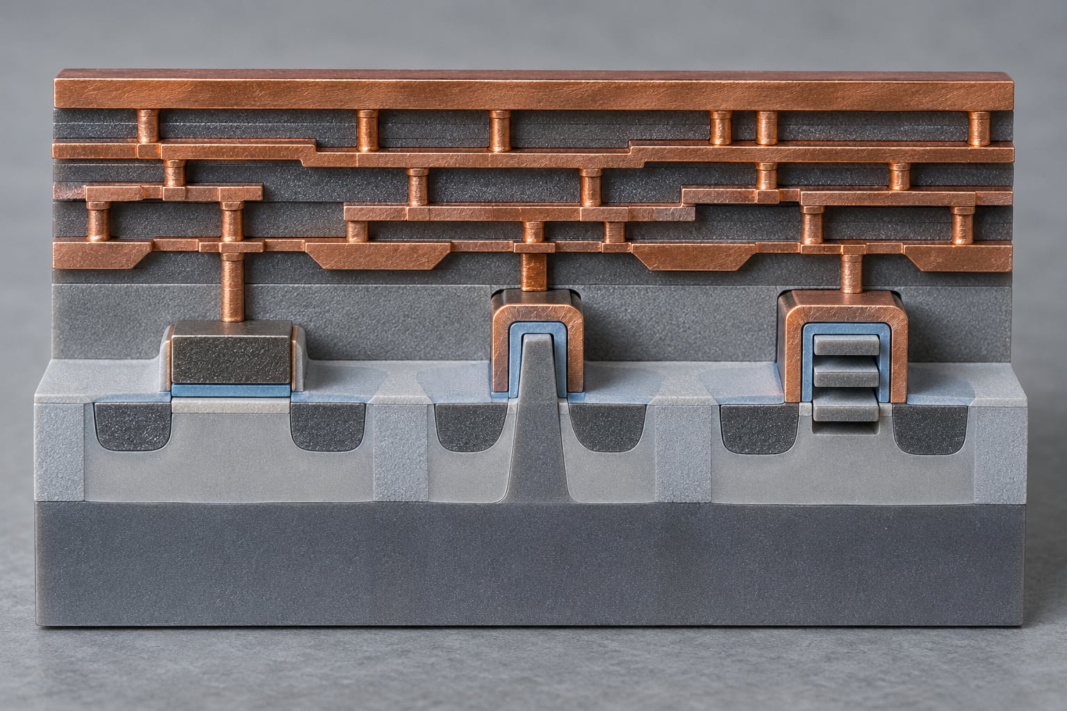
A cross-sectional view of modern transistor scaling
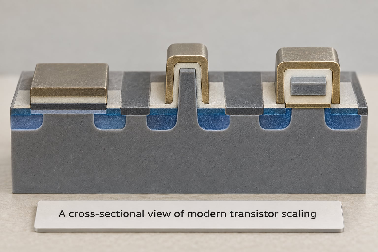
Cut a chip across its thickness and the progression is easy to read, because each generation changed the shape of the silicon rather than only its size. In a planar device the channel is a flat ribbon at the surface with a gate above it, which is why leakage climbed as the ribbon got shorter. In a FinFET the ribbon stands up as a fin and the gate wraps the top and both sides. In a gate-all-around device the channel becomes a thin horizontal sheet with a gate on all four faces, including the previously impossible underside.
The substrate underneath stays the same the whole way through, which is the point. Layers added later, backside power, buried power rails and stacked device layers fill vertical space that was previously empty, and that is where the geometry work has moved.
Where atomic scale changes transistor behavior
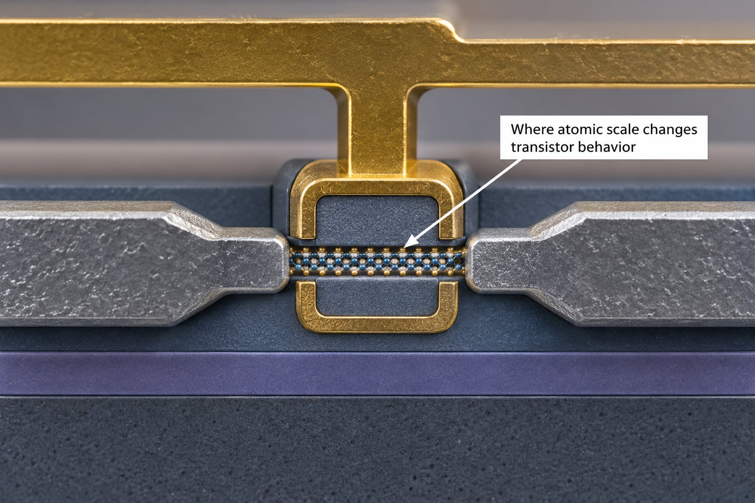
Zoom in on one transistor and four things stop being abstract. First the channel: at a few tens of atoms long, the count of atoms decides whether the device is fast, which is why foundries now vary sheet width deliberately rather than fighting for a single perfect number. Second the gate dielectric: below a few atomic layers, tunnelling through the insulator itself becomes measurable, which is the reason a high-k material is used so the physical layer can stay thick while the electrical thickness shrinks. Third the contacts: as the source and drain get smaller, the contact area falls and contact resistance rises, and it now sits in series with the transistor the design depends on. Fourth heat: the same switching energy in a smaller area means more heat per square millimetre, and the hottest spots are often at the contacts and in the interconnect rather than in the channel.
Frequently Asked Questions
Is Moore’s law the same as transistor scaling?
No, though the terms are used interchangeably. Moore’s law is an observation about density: the number of components on an integrated circuit doubling roughly every two years. Transistor scaling is the engineering work that produced those gains, shrinking dimensions and raising density. Density, speed and cost per transistor have not moved together since around the mid-2000s, so a node can deliver high density without delivering more clock speed.
What does a 3 nm or 2 nm process node actually mean?
It is a generation label, not a measured dimension. A node name tells you which family of process a design targets, roughly how much it may be reused for, and where it sits in a fab’s roadmap. It does not mean the gate is 3 nm or 2 nm long. The closest published geometric measure is the contacted gate pitch, which is larger than the node name. Treat node names as shorthand for a process generation.
Why can’t transistors keep getting smaller indefinitely?
Because several limits bind at once and push against each other. Shorter channels leak through the barrier once tunnelling and short-channel effects take over, and holding leakage down needs a higher threshold voltage, which cannot rise forever. Wires resist more as they narrow, so delay grows. Heat per unit area rises with density, and cooling caps how many transistors can run at full speed. Capital and design cost rise faster than the returns for most customers.
Are transistors physically shrinking as quickly as process-node names suggest?
Not at all, and the gap has widened. Transistor dimensions have continued to shrink, but the shrinking is uneven and increasingly vertical. Dielectrics, channel geometry and wiring changed differently, and much of the recent progress came from stacking, chiplets and more wiring layers rather than from a uniform lateral reduction. Naming a node after a shrinking number continued even after the correspondence with real dimensions broke down, which is why the label alone tells you very little.
Does advanced packaging mean chips are not getting smaller?
Not quite. Packaging adds to a system’s smallest dimension rather than removing it, but it changes what the smallest relevant unit is. When a processor, its cache and its I/O are separate dies in one package, the whole assembly is the product and no single die has to be as large. It also lets each die use the cheapest process that works for it, so cost per function can fall even as physical size does not.
Conclusion
The reason scaling is slowing down is not one wall but four constraints arriving together: a voltage floor that stops short channels from switching cleanly, leakage and heat that cap how many transistors can run at once, interconnect resistance that eats the gains a smaller transistor would have delivered, and a rising cost of building and designing each generation. To understand how transistors shrink and why scaling is slowing down, hold onto that: the old lever, drawing a smaller shape, is now only one of several, and it is the most expensive one.
What the industry is doing instead is selective. Channel and gate structures keep improving where they pay for themselves, materials like two-dimensional semiconductors replace silicon where the silicon body is too thick, and performance is assembled from chiplets, stacked layers and purpose-built accelerators instead of one giant uniform die. For anyone planning compute capacity beyond 2026, plan on gains that arrive in steps, spread across packages and specialised hardware, rather than a smooth doubling every two years.