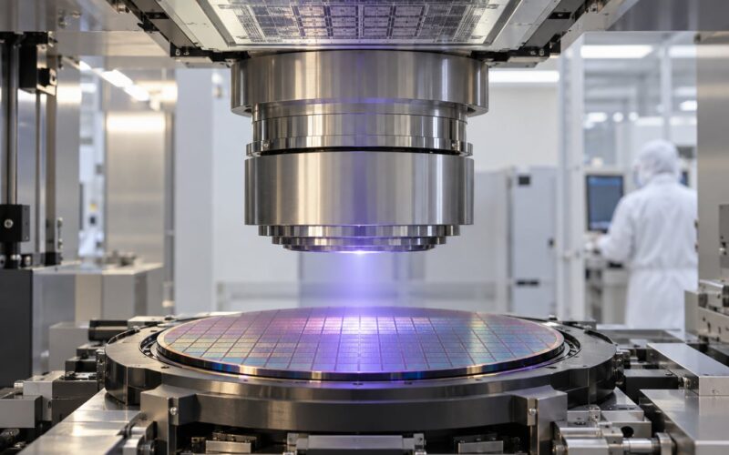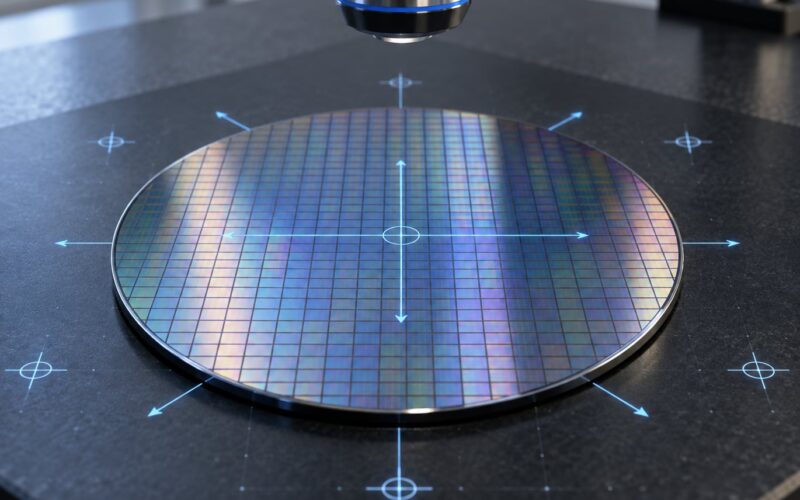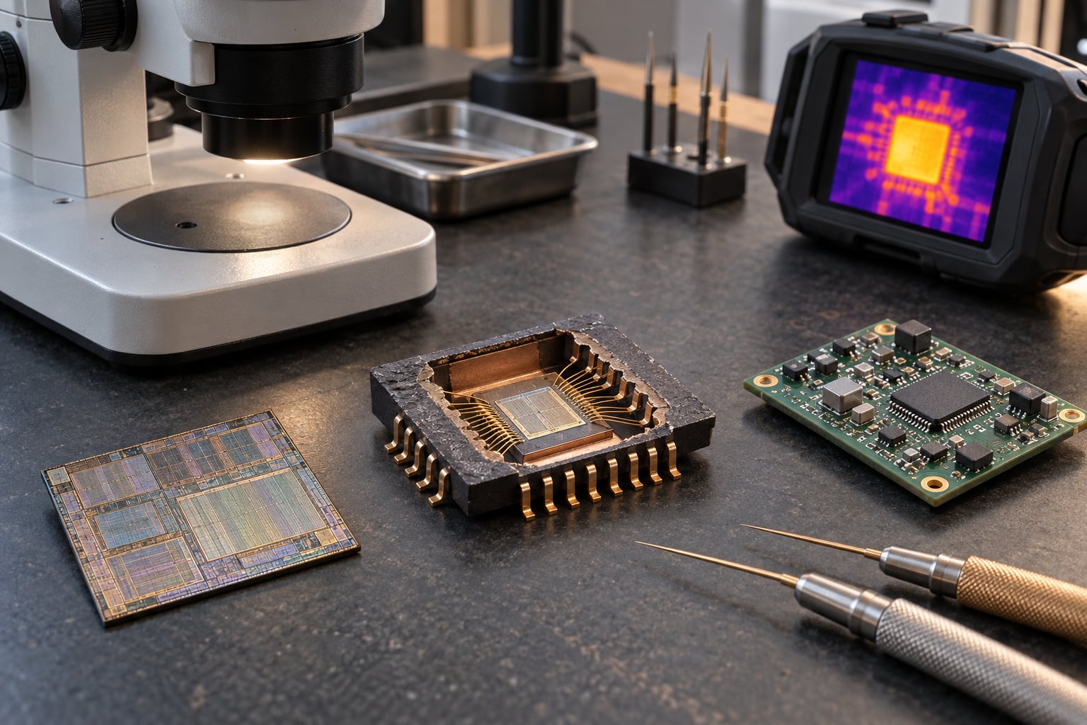
Semiconductor failure analysis is the systematic investigation of why an integrated circuit, its package, or the board around it stopped meeting specification. Failure analysis methods for chips explained properly means working backward from an observed symptom to the physical defect that produced it, and from that defect to the process step, material, or design margin that let it happen.
The most useful way to organize the methods is not by equipment brand or by whether they use a laser. It is by the question each one answers. Some tools tell you the part is broken. Some tell you where on the die the damage sits. Some tell you what the material at that spot actually is. The investigation is done when those three answers line up.
Table of Contents
- What Is Chip Failure Analysis? The Systematic Search for a Physical Cause
- Why Do Chips Fail? Seven Categories With Distinct Signatures
- Which Failure Analysis Method Should You Use? Start With the Least Destructive Step That Answers the Question
- Electrical Failure Analysis Methods: Confirm and Classify Before You Look Inside
- Optical and Physical Inspection Methods: See the Defect Without Consuming the Part
- Thermal, Timing, and Environmental Analysis: Find the Hot Spot and the Timing Signature
- Chemical and Material Analysis Methods: Identify What the Part Is Actually Made Of
- How to Perform Failure Analysis Step by Step: A Five-Stage Workflow
- Failure Analysis Methods for Chips: From Symptom to Root Cause
- How to Choose Between Lab and In-House Analysis: Match Capability to the Question
- What Evidence Proves a Root Cause? Correlation, Localization and Controlled Reproduction
- Frequently Asked Questions
- Which method is best for finding an intermittent chip failure?
- When should destructive analysis be used on a semiconductor?
- Can chip failure analysis recreate the original operating conditions?
- What is the difference between failure analysis and ordinary electrical testing?
- How long does semiconductor failure analysis usually take?
- Can a software simulation prove the root cause of a chip failure?
- Conclusion
What Is Chip Failure Analysis? The Systematic Search for a Physical Cause
Chip failure analysis combines electrical testing, non-destructive imaging, fault localization, and materials characterization to move from a failure mode to a failure site, a physical mechanism, and a root cause. It is a science, not a service call, because the same symptom can come from opposite causes and only physical evidence separates them.
That distinction matters. Electrical test tells you a device is out of specification. Failure analysis tells you why, and puts the reason somewhere you can fix. Debug does the first job. Failure analysis does the second.
Four terms do most of the work in a report, and mixing them up is the fastest way to a wrong conclusion.
| Term | What it means | Example |
|---|---|---|
| Failure mode | The observed symptom, in the words of the test that caught it | Leakage current 40x above the limit at room temperature |
| Failure site | The physical location of the defect on the die or in the package | One metal-2 via, 0.3 micrometers wide, adjacent to a poly resistor |
| Failure mechanism | The physical process that damaged the device at that site | Electromigration voiding in the via after sustained high current density |
| Root cause | The upstream reason the mechanism was allowed to run | A current density spec exceeded during a high-temperature burn-in profile |
Note the distance between the top row and the bottom one. The mode is measured in amps. The root cause is a decision somebody made in a process flow document, and no microscope reaches it directly. It has to be argued from evidence.
Why Do Chips Fail? Seven Categories With Distinct Signatures
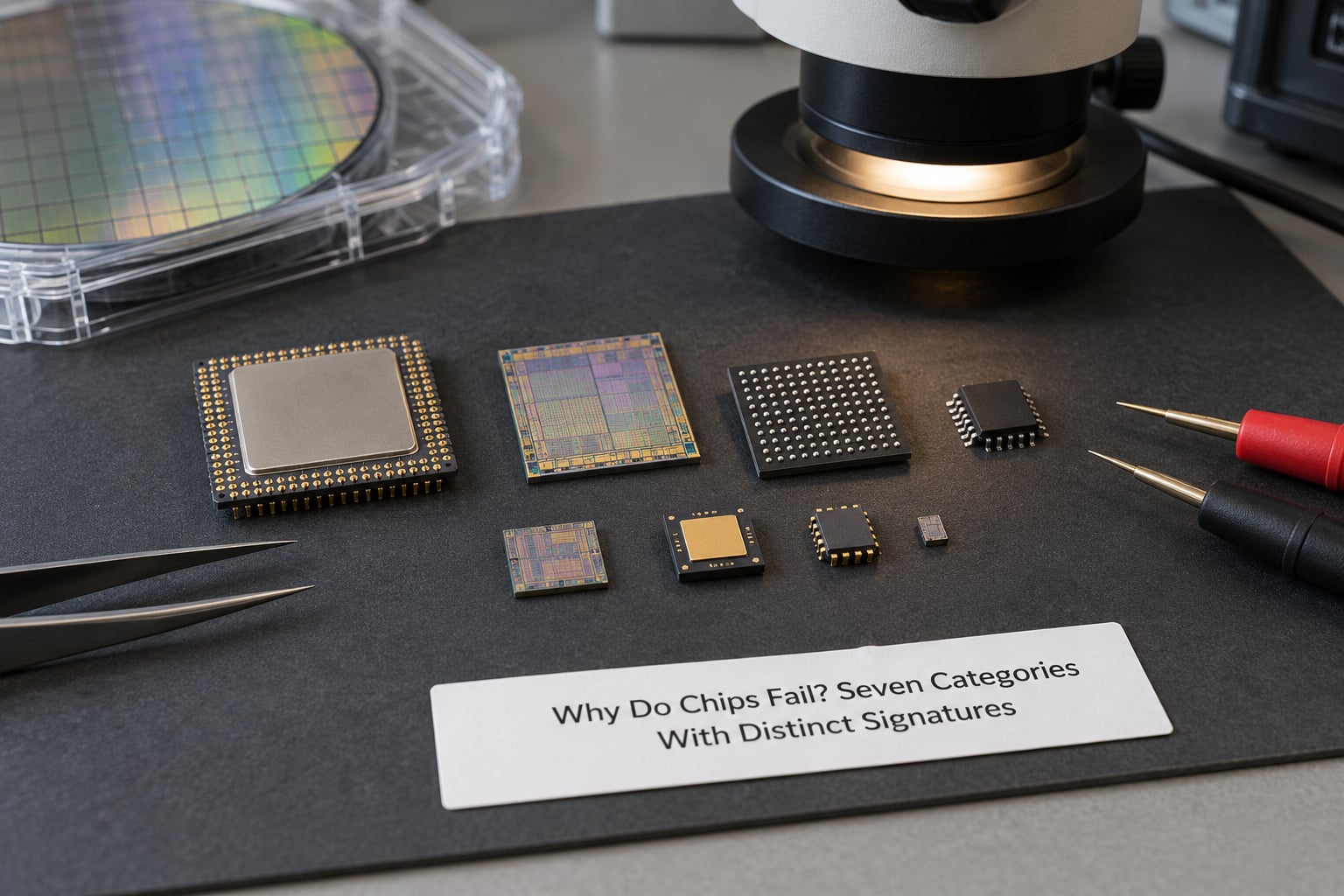
Failures cluster into a handful of categories, and each one leaves a signature that narrows the method choices. Knowing the category up front often saves a week of work, because a wire bond failure and a gate oxide breakdown call for completely different first tools.
| Category | Typical mechanism | Signature you observe |
|---|---|---|
| Electrical overstress | Supply rail exceeded, output shorted, hot-plug transient | Total failure, localized melt or soot near a driver pin, several adjacent cells damaged |
| Electrostatic discharge | Fast high-voltage event through a thin dielectric | Single pinpoint dielectric puncture, or a junction path at a pad edge |
| Thermal | Junction overheating, heat sink failure, thermal cycling fatigue | Output current droop with temperature, cracks radiating from a die corner |
| Mechanical and thermomechanical | Die crack, substrate flex, package stress, vibration fatigue | Failure correlated with temperature swing or board flex, visible crack on cross-section |
| Process defect | Mask defect, etch residue, via slump, missing fill | Random yield loss across a wafer, defect captured in a reliability monitor structure |
| Materials and contamination | Particle migration, corrosion, mobile ion drift, delamination | Drift over time at humidity, discolored bond pad, acoustic void at the die attach |
| Design marginality | Spec met in simulation, not in silicon | Failure appears only at high temperature and high frequency, or only at one supply corner |
Most real investigations cross categories. A part that fails in the field after two years of humidity exposure often has a package-level entry path and a design that did not expect it, which is why the report has to name a root cause rather than just a victim.
Which Failure Analysis Method Should You Use? Start With the Least Destructive Step That Answers the Question
Choose the method by asking what you need to know, not by what the lab owns. The table below maps the main analytical questions to the methods that answer them, along with the limitation that bites engineers most often.
| Analytical question | Representative methods | What it reveals | Key limitation | Destructive |
|---|---|---|---|---|
| Is the part really failing? | Automated test equipment, functional test, parametric test | Pass or fail, and which pins or bits are involved | No physical evidence at all | No |
| Is the failure inside the package? | X-ray radiography, X-ray CT, scanning acoustic microscopy | Voids, delamination, bond position, cracked die | Metal routing masks the defect it hides | No |
| Where on the die is the fault? | Emission microscopy, OBIRCH, TIVA, lock-in thermography | A light, current, or heat signature at a specific coordinate | Weak defects at advanced nodes give little signal | No |
| What does the damage look like? | Optical and scanning electron microscopy | Melting, cracking, missing features | Surface only unless sectioned | No, until sectioned |
| What is the material at that spot? | EDS, SIMS, XPS, Auger, Raman, XRD | Elemental and chemical identity, depth profile | Sample must stay flat and clean | Usually |
| What does it look like underneath? | Cross-sectioning, FIB-SEM, TEM | The internal stack, the interface, the crystal lattice | Consumes the sample and may create artifacts | Yes |
One rule sits underneath this table: non-destructive methods first. A technician in a failure analysis lab would put it more bluntly. Once the encapsulant is etched away, you cannot put it back, and the evidence that told you where to look may no longer exist.
Electrical Failure Analysis Methods: Confirm and Classify Before You Look Inside
Electrical testing is where every investigation starts, and its job is to turn a vague complaint into a specific mode. Without a clean classification, imaging teams are shooting in the dark with expensive tools.
Functional test asks whether the circuit performs its function, typically at speed on a tester with a known-good pattern set. A wrong output bit on a data bus is a strong clue and a weak one. Parametric test measures DC characteristics at specified conditions: leakage current, output drive, threshold voltage, resistance. Parametric failures are often more diagnostic than functional ones, because a leaky or slow pin points at a circuit block rather than a bit pattern.
Curve tracing goes further, sweeping a pin from a negative to a positive rail and plotting the current response. A Schottky diode, a transistor junction, a resistive path to the rail, and a leak to substrate all have different curve shapes, so a single trace can identify a part type that the netlist says should not exist on that pin. Capacitance-voltage measurement does the same job for oxide quality, reading out trapped charge and interface state density.
Power and ground checks deserve their own step. A part that fails only at a hot rail may be a victim of a bad board, not a bad chip, and the fastest way to tell is to compare the supply at the die pad against the supply at the connector. Scan chains, most often boundary scan, let a controller drive and read individual pads without powering the logic, which is how intermittent faults get caught on a part that passes every functional pattern when it is warm and fails when it is cold.
Intermittent faults are the hardest category, and engineers describe the search honestly: repeat the failing condition while varying one variable at a time, supply voltage, temperature, clock frequency, and board flex are the usual four. If the fault only appears when two conditions coincide, the search space collapses fast. If it appears at random, you can burn days before getting a single reproduction.
These tests are also the trigger point for everything downstream. Reliability programs define the trigger in writing. JEDEC JESD22 covers individual stress methods, JESD47 defines the qualification plan for integrated circuits, MIL-STD-883 governs military microelectronics test methods, and AEC-Q100 sets the automotive stress requirements. When a part fails one of those tests, the failure analysis scope is defined by what the standard says was being measured.
Optical and Physical Inspection Methods: See the Defect Without Consuming the Part
Non-destructive imaging is about finding a defect you can still examine chemically afterwards. That is why package-level work comes before die-level work, even when the symptom looks like a core problem.
X-ray radiography gives a 2D projection of the whole stack: die attach fill, wire and flip-chip bonds, substrate routing, and the void distribution under a solder joint. X-ray computed tomography builds a 3D volume from many angles and can find a delamination that a single projection hides behind dense metal. Scanning acoustic microscopy uses an ultrasonic pulse through the package and reads the echo, which makes it the standard method for finding delamination and voids at the die attach and under the mold compound, because acoustic contrast distinguishes an interface from intact material even when the optical contrast is nil.
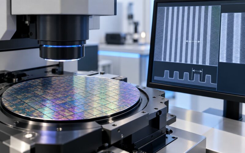
On the die, optical inspection catches the obvious things: a lifted wire, a cracked bond pad, a visibly darkened region. Scanning electron microscopy moves to nanometre resolution and shows melt, cracks, missing features, and the residue that an electrical overstress event leaves behind. Transmission electron microscopy goes one level deeper still, resolving interfaces, gate oxide thickness, and the crystal lattice itself, which is how a diffusion problem gets separated from a mechanical one.
Reaching those views requires opening the package, and there are three preparation routes with different consequences.
| Preparation route | What it removes | Use it when |
|---|---|---|
| Decapsulation | Mold compound, leaving pads and the top of the die exposed | You need bond pads, top metal, or a die surface to look at |
| Deprocessing | Passivation, dielectric, and metal layers, one at a time | You need to expose an internal layer, such as via arrays or a buried via |
| Cross-sectioning | The part is cut, polished, and viewed edge-on | You need the internal stack, an interface, or a defect below the surface |
Every one of those routes can manufacture the evidence you then interpret. Laser decapsulation leaves a heat-affected zone. Ion milling polishes with a preferred orientation. A cross-section through a stressed part can propagate an existing crack a few micrometers further and make the damage look worse than it was. Experienced analysts run a prepared-but-unfailed sample through the same process as a control, and any competent report tells you whether they did.
Thermal, Timing, and Environmental Analysis: Find the Hot Spot and the Timing Signature
Fault localization is the step where a part stops being a measurement result and starts being a coordinate. Most methods work by applying energy to the device and watching what responds.
| Method | Signal it detects | Good at finding | Limitation |
|---|---|---|---|
| Emission microscopy (EMMI) | Infrared light from hot carriers | Leakage paths and shorted nodes, single transistors | Needs a powered, warm device; blind to purely resistive defects |
| OBIRCH | Current change induced by a scanned laser | Leakage through a thin dielectric, gate oxide defects, resistive shorts | Slow; resolution degrades as the defect sits deeper |
| TIVA | Infrared image of thermally induced voltage change | Defects under the top metal, where a laser cannot reach | Heats the part, which can move a marginal defect |
| Lock-in thermography | Periodic heat at a fixed excitation frequency | Thermal signatures in packages, power devices, and mounted boards | Surface temperature only; cannot see inside encapsulation |
Optical beam induced current change, usually shortened to OBIRCH, is worth explaining because it is the most requested single technique in this list. The lab scans a focused laser across the die in a raster while the part is biased. Where the beam lands on a resistive or leaking path, the current drawn from the supply changes by a measurable amount, and the image that results maps current change against position. That is how a gate oxide defect a few nanometres thick, far too small to see optically, becomes a bright pixel with a coordinate attached.
The trap is that a thermal camera alone will not settle it. Surface emissivity varies with surface finish and coating, reflections from a gold bond pad can look like a hotspot, and a good thermal camera resolves 25 micrometers when the defect is 0.2. Engineers separate the artifact from the signal by changing one variable at a time, usually the excitation frequency or the bias condition, and by confirming the same coordinate with a second method. If the hotspot moves when you change the frame rate, you were measuring the reflection.
Environmental methods answer a different question: does the failure depend on conditions outside the electrical test? Temperature cycling flexes the package and the die together and drives thermomechanical fatigue. Vibration and mechanical shock find weak bonds and marginal solder joints. Humidity and biased humidity testing expose corrosion, mobile ion drift, and delamination, where a part passes dry and fails after days at elevated humidity and bias. These are slow tests, and they are usually the reason a failure analysis takes weeks rather than days.
Chemical and Material Analysis Methods: Identify What the Part Is Actually Made Of
Once you have a coordinate, chemistry answers the last question: what is actually sitting there, and how did it get there. This is where contamination root causes are confirmed or ruled out.
Energy-dispersive spectroscopy rides on the electron microscope and identifies elements from the characteristic X-rays each one emits, with a detection limit in the parts-per-million range for the heavier elements. It answers questions like whether a residue on a failed output is copper from a wire or tin from a solder process, and whether the metal in a via is the intended tungsten or something that migrated in later. SIMS and its time-of-flight variant ionize the surface and count atoms by mass, giving a depth profile of a thin layer rather than a single bulk reading, which is how trace chlorine under a bond pad gets found. XPS measures binding energies of the top few nanometers and reads the chemical state, distinguishing metallic copper from copper oxide, and is the reference method for a delamination surface. Auger electron spectroscopy has similar surface sensitivity with better lateral resolution, useful when a defect is small. Raman spectroscopy identifies specific molecules by their vibrational fingerprint and is a fast way to confirm an organic contaminant. X-ray diffraction answers a crystalline question, such as whether a thin film is the intended phase or an unwanted one.
Surface inspection deserves separate mention because it needs no instrument at all. Decapsulated parts under an optical or electron microscope often tell the story on their own: a dendrite grown from an ion left behind, a corroded pad with a green halo, a ring of discoloration where a galvanic couple formed. A chemist looking at the right region with the right tool then confirms what the eye suspected.
Material analysis also has the power to disprove a hypothesis, which matters more than it sounds. A report that confirms contamination without ruling out mechanical damage is incomplete, because both can produce the same leakage signature.
How to Perform Failure Analysis Step by Step: A Five-Stage Workflow
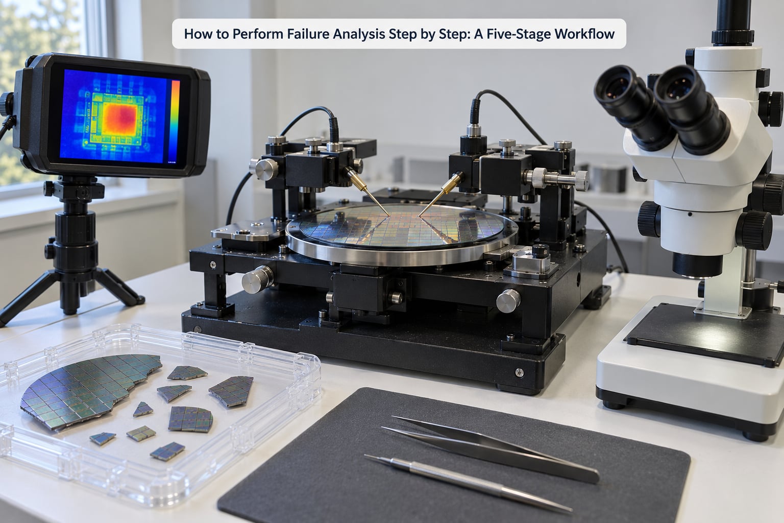
The order below is the same in most labs, and the reason for the order is the reason the whole discipline works: every destructive step destroys the evidence for the previous ones.
- Verify and document the failure. Reproduce the symptom on the test setup, record the exact conditions, supply rails, temperature, and the test pattern that failed. Pull the device history: wafer, lot, assembly site, package type, and any handling or rework in its past. Half of all investigations are short-circuited here, because the part fails on the bench in a way it never failed in the field.
- Run non-destructive analysis. Optical inspection for gross damage, then X-ray radiography and scanning acoustic microscopy for package integrity. A void, a cracked die, or a lifted wire found at this stage often needs no further work at all.
- Localize the fault. If the part is electrically alive, use emission microscopy, OBIRCH, thermography, or electron beam probing to get a physical coordinate on the die. If the part is dead or intermittent, use probe-point or continuity mapping to narrow it to a block.
- Perform destructive physical analysis. Decapsulate, deprocess, or cross-section only after the non-destructive work is finished and documented. Section through the localized coordinate, then image with electron microscopy, and analyze composition at the site.
- Establish root cause and report. Correlate the physical evidence with process, design, and reliability data, state the mechanism, name the upstream reason, estimate how many parts in the population are affected, and recommend corrective action with evidence for each claim.
Failure Analysis Methods for Chips: From Symptom to Root Cause
Consider a mixed-signal controller that ships clean and shows rising field returns after months in service. About 4% of returned units draw noticeably more standby current than specification, and the returns cluster in parts assembled at one site.
Stage one reproduces it. The parts pass functional test at room temperature but fail their leakage limit at 60 degrees C, which moves the failure from functional to parametric and immediately suggests a temperature-dependent resistive path. Stage two finds nothing at the package level. X-ray shows normal die attach fill and intact bonds, and acoustic imaging shows no delamination.
Stage three supplies the coordinate. Emission microscopy at elevated bias shows light from one analog block, and a laser scan at the same condition confirms a current change that lines up with a resistive path on the internal supply rail of that block, not the digital core. That rules out a board or supply problem and puts the investigation on the die.
Stage four opens the part. A focused ion beam cross-section through the coordinate shows an open via in the metal stack, the via filled with a mottled, low-density material rather than solid tungsten. Backscattered imaging makes it obvious this is not a designed open, and energy-dispersive spectroscopy finds copper and fluorine in the fill. A separate surface scan of a second returned unit finds the same copper halide residue on the passivation near the assembly site’s clean line. Stage five ties it together: a cleaning residue introduced copper and fluorine species, they migrated under bias and temperature toward the biased analog rail, and the electrochemical reaction removed the via fill.
The mechanism is electromigration-assisted voiding driven by mobile contamination. The root cause is the process, not the chip design. The corrective action is a change to the cleaning step and a bias on the analog rail ordering, and the population estimate comes from the assembly site and the return rate rather than from a guess.
What makes that conclusion defensible is not the microscopy. It is that the same residue, the same chemistry, and the same failure signature appeared in a second part from the same site, and the temperature dependence matched the mechanism.
How to Choose Between Lab and In-House Analysis: Match Capability to the Question
Most organizations do some analysis in-house and send the rest out, and the split is usually decided by equipment capital rather than by what is sensible. It helps to look at the tiers by what each one is actually for.
| Route | Best suited to | Turnaround | Tradeoff |
|---|---|---|---|
| Internal screening and test | Confirming a failure, parametric trends, lot-to-lot comparison | Hours to a few days | Cannot localize a fault; the answer stops at “fails” |
| Design team debug | Reproducing silicon issues, comparing against a known-good unit | Days | Strong on the design side, usually no microscopy or materials capability |
| Independent failure analysis laboratory | Field returns, qualification failures, independent evidence | Days for electrical work, weeks for full physical analysis | Cost per step, and you must brief them well |
| Specialist equipment centre | FIB, TEM, SIMS, and other tools too costly to own | Queued, often weeks | Longest path, and the sample is consumed |
Turnaround is where the planning matters. An electrical-only investigation can close in a few days. Adding localization extends it, and adding cross-sectioning with electron microscopy and materials analysis routinely pushes a case into the multi-week range, because those tools are run by specialists with limited sample throughput.
Cost follows that same ladder, and it is worth pricing the whole investigation rather than the individual step. A local check that comes back negative is cheaper than a laser localization run that finds nothing, but it can also cost weeks of delay. The expensive mistake is not paying for a technique. It is ordering the techniques wrong and having to restart, or paying for a full physical analysis on a part that had a cracked die visible on the first X-ray.
Confidentiality and independence are worth weighing too. A design team will know the full design intent and can interpret a signature quickly, but an independent lab gives you evidence that survives a customer or legal dispute, which matters for automotive and medical work.
What Evidence Proves a Root Cause? Correlation, Localization and Controlled Reproduction
Reading a failure analysis report well means sorting each sentence into evidence or interpretation. The distinction is usually clear in good reports and blurred in bad ones.
Evidence is something that was measured and can be checked: the leakage curve, the X-ray image, the emission micrograph with its coordinates, the cross-section showing a void, the elemental spectrum showing copper, the second unit from the same lot with the same residue. Interpretation is the engineer’s reading of that evidence, and it should be labeled as such.
A root cause holds up when several of these conditions are met together. The failure is reproduced under controlled conditions rather than inferred from a return report. The site is localized spatially, at a named coordinate, and the mechanism observed there is consistent with the electrical symptom measured earlier. The material identified matches the mechanism proposed. A known-good or unstressed control, prepared the same way, does not show the same feature. And the competing explanations have been tested and eliminated, not just ignored.
When a report is thin, the misses are recognizable. A mechanism named from a single image with no control sample. A root cause that stops at “process variation” without pointing at the step. An explanation that ignores the temperature or humidity dependence the data clearly shows. A conclusion drawn from a part that was already destroyed by handling before it arrived.
A practical question to ask any lab: what else did you consider and rule out, and what evidence ruled it out. The answer tells you more about the investigation than the conclusion does.
Frequently Asked Questions
Which method is best for finding an intermittent chip failure?
No single method wins, and the sequence matters more than the tool. Start by reproducing the failure while varying supply voltage, temperature, clock frequency, and board flex one variable at a time, because an intermittent tied to two conditions is far easier to catch. Electrical curve tracing and probe-point mapping narrow the failing block, then emission microscopy, OBIRCH, or thermography gives you a coordinate on the die. Keep the part unopened until that coordinate exists, because decapsulation first destroys the evidence.
When should destructive analysis be used on a semiconductor?
Destructive methods such as deprocessing, cross-sectioning, FIB, and TEM should be used only after every non-destructive step has run and been documented. If optical inspection, X-ray radiography, scanning acoustic microscopy, and fault localization have already been completed, destructive analysis becomes the correct tool for the one question they cannot answer: what the internal stack or material at a known coordinate actually is. Decapsulating early is the most common and most expensive sequencing error in the discipline.
Can chip failure analysis recreate the original operating conditions?
Partly, and the gap is worth stating in any report. Electrical conditions can usually be reproduced closely: supply voltage, frequency, temperature, and bias are all set on the bench. Mechanical and environmental histories are harder, since a part that failed after 500 temperature cycles cannot have those cycles replayed, only approximated with accelerated stress. That is why analysts weight the unit’s history and the return data heavily when the bench conditions only partly reproduce the symptom.
What is the difference between failure analysis and ordinary electrical testing?
Electrical testing answers whether a part meets specification, and it can be automated and run on every unit in a lot. Failure analysis answers why a specific part did not, using imaging, fault localization, and materials characterization to reach a physical site, a mechanism, and a root cause. Testing alone gives you a pass or fail bit. Failure analysis turns that bit into evidence that can change a process step, a package design, or a design margin.
How long does semiconductor failure analysis usually take?
An electrical-only investigation can close in a few days. Adding fault localization extends that, and a full physical analysis with cross-sectioning, electron microscopy, and materials work commonly runs several weeks, partly because specialist instruments are run by people with limited sample throughput. A controlled reproduction of an intermittent failure can add days of its own. Ask for a written plan with milestones, and know that the scope changes most often because a part could not be reproduced on arrival.
Can a software simulation prove the root cause of a chip failure?
No. Simulation can show that a design is marginal at a supply corner or a temperature extreme, and that is genuinely useful, but it runs on the model you built rather than on the part that failed. Root cause requires physical evidence from the failed device: a localized site, an observed mechanism, and an identified material. Simulation narrows where to look and predicts the signature to expect, then the microscope and the spectrometer do the proving.
Conclusion
Failure analysis methods for chips explained comes down to one selection rule: use the least destructive technique that can still answer the question in front of you, and never skip a step that the next one depends on.
Start with the paperwork. Document the exact failure, the conditions, and the device history, then reproduce it on the bench before a single tool touches the part. Once the symptom is classified as functional or parametric, you know which method family to reach for, and from there the investigation moves from coordinate to cross-section to chemistry until the mechanism and the root cause are the same statement. Updated for 2026, this guide reflects the standard lab practice at most independent failure analysis organizations.