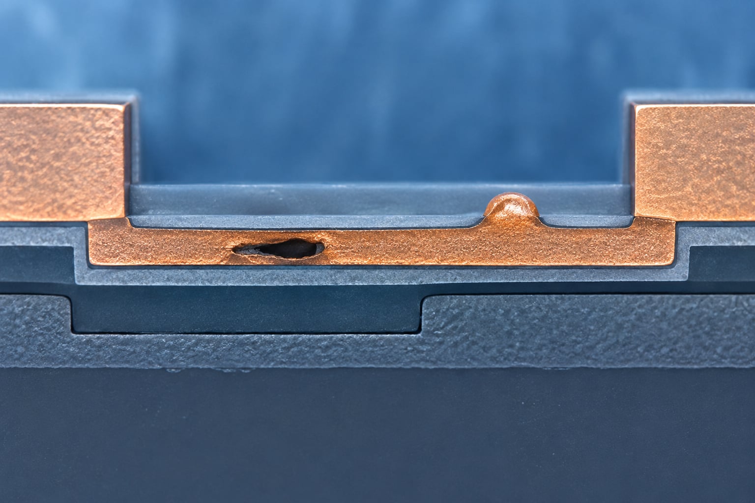
Electromigration is the slow, permanent movement of metal atoms inside a conductor, driven by momentum transfer from electrons that are flowing through it. Inside an integrated circuit, that drift hollows out voids in the metal lines and vias that carry power and signals between transistors, and the voids eventually cut the connection. What electromigration is and why it kills chips comes down to one number: current density. In copper and aluminum on-chip interconnects it routinely runs between 106 and 107 A/cm2, and that is far past the point where the metal stops being stable.
The mechanism is well understood, documented, and modeled. Black’s equation, published by J.R. Black at Motorola in 1969, still gives engineers a usable lifetime estimate, and every foundry ships current-density limits in its design rule manual. So this is not an exotic defect. It is a wear-out mechanism with a known cause, and it stays in the news because a chip that survives every test at day zero can still open up in the field after a few years of ordinary use.
Table of Contents
- What Is Electromigration in an IC?
- How Atoms Move Inside a Metal Interconnect
- What Drives Electromigration?
- How Does Black’s Equation Relate to Electromigration?
- Why Does Electromigration Kill a Chip?
- How Voids and Resistances Become Electrical Failures
- Which Chip Failures Are Caused by Electromigration?
- How Designers Prevent and Test for Electromigration
- Material and stack choices
- Layout rules
- Signoff and EMIR checks
- Qualification testing
- Frequently Asked Questions
- Is electromigration the same thing as electrical overload?
- What physical damage does electromigration cause inside a chip?
- Does electromigration happen quickly during normal chip operation?
- Why do vias and narrow metal lines experience more electromigration?
- Can electromigration be detected before a chip fails completely?
- Key Takeaway
What Is Electromigration in an IC?
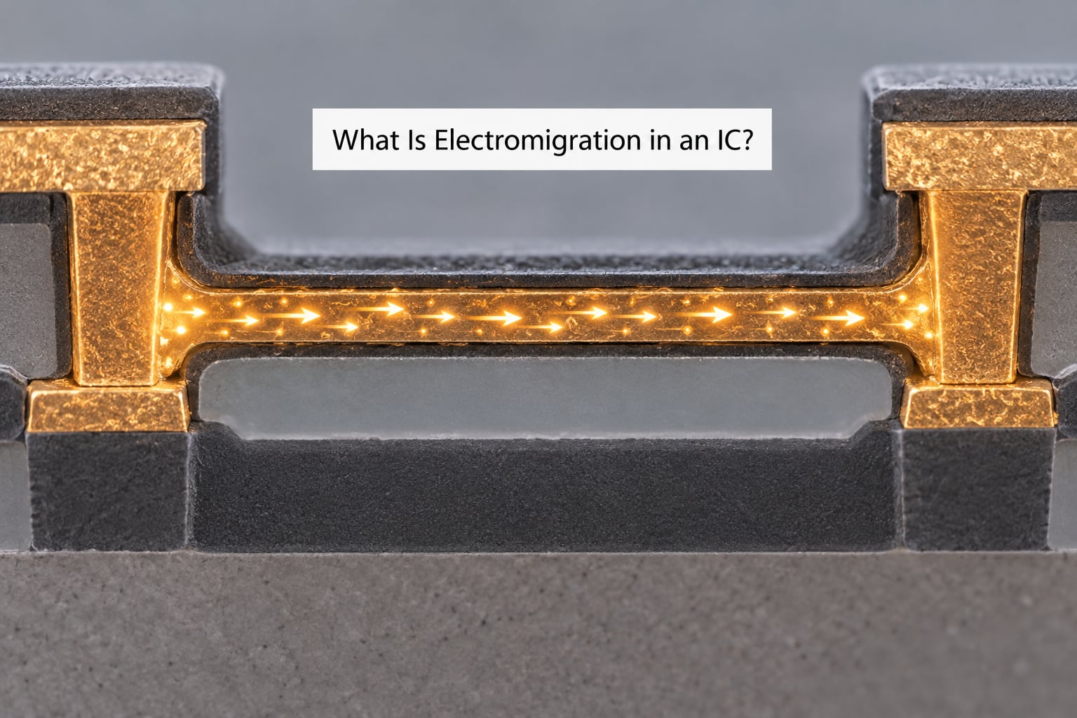
Electromigration, usually shortened to EM, is the gradual transport of metal atoms caused by collisions between conducting electrons and the metal atoms they pass. At high current density, atoms drift in the direction of electron flow, leaving voids behind at the cathode end and piling up as hillocks at the anode end. The voids open circuits. The hillocks short adjacent lines.
It is worth separating that from three things it gets confused with. Ordinary current flow does not move mass: electrons carry charge, the lattice stays put, and copper still works after ten billion amps have passed through it. Electrostatic discharge is a single, violent event that punches a hole through a junction or blows a gate oxide, typically in nanoseconds. Dielectric breakdown is a field-driven insulation failure inside the oxide. Electromigration is none of those. It is slow, cumulative, and driven by a combination of current density and temperature acting for years.
What makes it dangerous for a chip specifically is the environment it happens in. An interconnect line in a modern IC might be 20 nm wide and only 50 nm thick, buried between layers of low-k dielectric that conduct heat away poorly. The same current pushed through a fat power cable in a server is nothing. Pushed through a line that thin, it is an enormous density.
How Atoms Move Inside a Metal Interconnect
Atoms move because electrons hit them. A free electron drifting through the lattice collides with a metal ion and transfers momentum to it. In a perfect single crystal this force is symmetric and the net effect largely cancels. Real interconnect is not a perfect crystal, and that is where the damage starts.
Polycrystalline metal is a patchwork of small grains at different orientations. Grain boundaries are where atoms are weakly bonded and where diffusion is fast. The first thing to go is a spot where a boundary meets the top or side surface of the line, a corner, or a via boundary. A vacancy opens there, nearby atoms shuffle into it, and the vacancy walks. Once enough vacancies cluster, a void nucleates.
Three diffusion paths compete, and they respond differently to temperature and geometry. Grain boundary diffusion runs along the boundaries themselves and dominates at lower temperatures. Surface diffusion runs along the top of the metal and matters most in narrow lines where the surface is close to the path. Bulk diffusion, where atoms hop vacancy to vacancy through the interior of the grain, takes over at high temperatures.
The force itself is usually written as a product of the current density, the metal’s resistivity, the effective valence Z*, and the atomic volume. The effective valence is a fitted parameter that captures how efficiently the crystal converts electron momentum into atom motion; it is not simply the number of valence electrons. Then there is a second term that pushes the other way: mechanical stress. A region under tensile hydrostatic stress holds atoms more tightly, and the resulting back stress partially cancels the electron wind.
Net atom flux is the difference between those two. Where flux is high, atoms leave. Where flux is zero, nothing happens. That balance is why Blech’s length matters: below a certain conductor length, back stress wins and the line is effectively EM immortal, because atoms are driven off the ends faster than the electron wind can pile them up.
Now the part that surprises people. Interconnects have been getting smaller for four decades, and smaller interconnects were supposed to be safer. They were not, because the current they carry did not shrink at the same rate as their cross-section. When width and thickness both halve, area drops to a quarter while current stays roughly the same, so current density doubles. Chips did not become more fragile because the physics changed. They became more fragile because the same amps were forced through a smaller pipe.
What Drives Electromigration?
Current density and temperature dominate everything else, but the list of contributing factors is longer than most people expect. Here is what each one actually changes.
| Driver | What it does | Relative effect |
|---|---|---|
| Current density (J) | Sets the electron wind force and therefore the atom flux | Dominant; lifetime scales roughly as J-n with n between 1 and 2 |
| Temperature (T) | Raises atomic mobility and lowers the effective diffusion barrier | Very strong; an Arrhenius exponential in 1/T |
| Conductor material | Sets activation energy and effective valence | Activation energy is about 0.7 eV for aluminum, 0.9-1.1 eV for copper |
| Line width and thickness | Determines cross-sectional area, and therefore J | Halving both dimensions roughly doubles J at constant current |
| Via and contact resistance | Diverts current around an opening, crowding it at the entry and exit edges | Local J can run several times the average line value |
| Mechanical stress | Produces back stress opposing the electron wind | Can make short lines effectively EM immortal |
| Interfaces and liners | Barrier and seed layers change which diffusion path is fastest | Cobalt, ruthenium and tantalum nitride liners change the failure mode entirely |
| Duty cycle | Bidirectional or pulsed current partly reverses atom flow | Alternating current is far gentler than the same DC current |
| Grain structure | Bamboo structure removes continuous boundary paths | Deliberate slotting of lines forces bamboo structure in narrow conductors |
How Does Black’s Equation Relate to Electromigration?
Black’s equation is an empirical model that turns those drivers into a single number: mean time to failure. In its common form, MTTF equals A multiplied by J to the power negative n, multiplied by the exponential of Ea over kT. A is a constant fitted to the conductor and geometry, J is current density, n is an empirical exponent, Ea is the activation energy, k is the Boltzmann constant, and T is absolute temperature in kelvin. J.R. Black published it in 1969, and while later work has qualified it, signoff flows still lean on it heavily because it is conservative and cheap to evaluate.
| Symbol | Meaning | Typical value or unit |
|---|---|---|
| A | Pre-exponential constant, geometry and material dependent | Fitted, hours times current density to the nth |
| J | Current density in the conductor | A/cm2 |
| n | Current density sensitivity exponent | 1 to 2, commonly about 2 |
| Ea | Activation energy for diffusion | 0.7 eV aluminum, 0.9-1.1 eV copper |
| k | Boltzmann constant | 8.617 x 10⁻⁵ eV/K |
| T | Absolute temperature | Kelvin |
What the equation tells you immediately is that the two multipliers compound. Taking a copper interconnect with Ea of 0.9 eV, raising the junction temperature from 100 C to 150 C shortens the mean time to failure by roughly 27 times. Doubling the current density at a fixed exponent of 2 cuts it by about 4 times. Do both at once and you have cut a design’s life by more than two orders of magnitude. That is why EM signoff always evaluates worst-case voltage, temperature and activity, and why a chip that passes at nominal has not actually been signed off.
| Change | Assumption | Relative MTTF |
|---|---|---|
| Baseline | 100 C, J, copper with Ea 0.9 eV | 1.0 |
| 150 C instead of 100 C | Same current density | About 0.04 |
| Current density doubled | Same temperature, n = 2 | 0.25 |
| Both changes at once | 150 C and doubled J | About 0.01 |
Black’s equation has a real weakness, and it is the one that matters at advanced nodes. It assumes a uniform conductor with a single dominant diffusion path. A modern copper line contains a cobalt or ruthenium liner, a barrier, a low-k dielectric interface and a via stack, and the fastest path is often along one of those interfaces. The model under-predicts damage there. That is part of why physics-based approaches, from atomistic kinetic Monte Carlo simulation up to TCAD electromigration models, have taken over the research conversation while Black’s equation remains the industrial baseline.
Why Does Electromigration Kill a Chip?
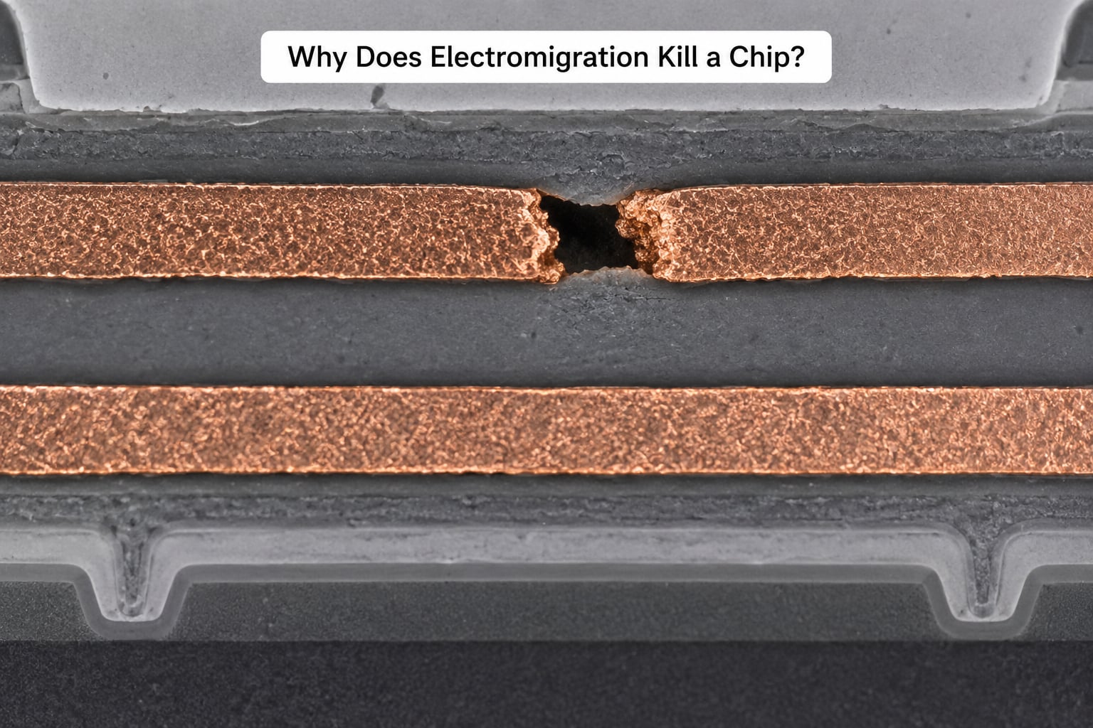
It kills chips slowly, quietly, and in a way that rarely gets diagnosed correctly. The damage runs through five stages, and the chip usually fails long before the last one.
- Current crowding. Nothing about a uniform line is uniform in practice. Current funnels into the narrowest section, spreads out where it meets a contact, and concentrates at the inner edge of every bend. Local current density at those points runs well above the average the designer calculated.
- Atom drift. The electron wind pushes metal atoms away from the cathode. Vacancies form where atoms leave.
- Void nucleation. Vacancies cluster at a grain boundary, a surface, or a liner interface until they merge into a small cavity, typically tens of nanometers across.
- Void growth. The void grows by absorbing more atoms. It usually spreads along the grain boundary, which is why EM damage looks like a slit rather than a hole, and it does not stop until it has consumed the full cross-section at that point.
- Open circuit. The line severs. Everything downstream of that point loses power or loses its signal path.
The parallel path runs the other direction. At the anode, displaced atoms accumulate instead of leaving, extruding metal out of the line and eventually out of the layer. Those extrusions are called hillocks. A hillock that grows far enough laterally bridges to the neighboring interconnect, and now you have a short. Shorts are less common than opens in most flows, but on a tightly packed analog layer they can be the more expensive failure, because a single bridged pair can take out a whole block of circuitry.
The field symptom profile is what makes this so frustrating to debug. A chip with a growing void does not fail cleanly. As the void constricts the line, resistance drifts upward, so the rail sags slightly under load. That produces intermittent glitches first: rare, load-dependent errors that pass every test at room temperature and vanish when the board is idle. Then individual vias start failing, errors cluster in time instead of spreading randomly, and finally the net opens outright. A part that looks like it has an intermittent logic bug in month fourteen is very often a part with an open interconnect.
It is a wear-out mechanism, not a defect. Which means the same part number from the same wafer lot can pass end test and still fail three years later, and the failure distribution is heavily skewed toward the tail of the population, not the average.
How Voids and Resistances Become Electrical Failures
A void is not a switch. It is a resistor that gets worse, and that feedback loop is the whole failure mechanism in miniature.
As the void narrows the conducting cross-section, resistance in that segment rises in proportion to the inverse of the remaining area. Higher resistance in a constant-current path means a bigger voltage drop across the segment. Less area also means the same current is squeezed through a smaller region, so local current density climbs again. Higher current density means more electron wind, which means more atom drift, which means a bigger void. Joule heating adds to it: the constricted segment dissipates more heat into a stack of low-k dielectric that was chosen for its insulation properties, not its thermal conductivity.
Each loop feeds the next. Most of the time the system absorbs it. A rail that sags 30 mV under a 10 mA load may simply give the downstream circuit a little less headroom, and nothing visible happens. Eventually a signal line crosses a timing threshold, or a logic state that depends on precise bias voltage flips at a temperature the part never sees during test, and the symptom is a glitch in a system that is otherwise behaving.
Four electrical signatures follow from that, in rough order of how often you will meet them:
- Rising resistance. The earliest measurable sign, and the one that makes accelerated EM testing work at all. Test structures are built with long resistive lines and monitored continuously; when resistance drifts by a set percentage, the test declares failure.
- Intermittent continuity loss. A partially open line that works at low load and fails at high load or high temperature. This is where the field-failure profile comes from.
- Drifting timing or voltage behavior. Soft errors and marginal timing on a single net, appearing only under thermal or load conditions.
- Excess current and localized heating. After a full open shorts out to a rail, current spikes through a path that was never sized for it. This is often the step that physically destroys the die, rather than the open itself.
That last point explains why the word burnout shows up in almost every description of this failure. EM opens a line. The system reacts to the open by pushing more current through surviving paths. Those paths then fail too, sometimes violently, and the failure analysis lab finds a crater rather than a clean break.
Which Chip Failures Are Caused by Electromigration?
EM is one of several mechanisms that degrade metal, and telling them apart in a failure analysis lab is mostly a matter of looking at where the damage is, what shape it is, and how long the part had been running. This table is the version I keep coming back to.
| Mechanism | Driving force | Signature | Timescale | Where it shows up |
|---|---|---|---|---|
| Electromigration | Current density plus temperature | Slit-shaped void along a grain boundary, or anode extrusion | Years to tens of years of operation | Cathode side of a via, narrow line, current crowding point |
| Stress migration | Mechanical stress relaxation, no current needed | Void in a continuous metal line or dielectric interface, no hillocks | Thousands of hours, can accelerate near a via | Wide, straight, low-current lines far from any high-stress via |
| Bias temperature instability | Electric field at the gate, elevated temperature | Threshold voltage shift, transconductance loss, no physical metal damage | Hours to years of bias | Transistor gate stack, not interconnect |
| IR drop | Resistance in the supply path | Voltage sag, no physical damage at all | Immediate, load dependent | Whole power grid; visible in dynamic voltage drop analysis |
| Electron migration and self-heating in a power device | Very high local current at a junction | On-resistance creep, thermal runaway | Hours to years | Source drain current path in a power MOSFET or IGBT |
Two practical rules fall out of it. If there is no physical metal damage at all, you are looking at IR drop or bias temperature instability, not EM. If there is metal damage with no hillocks, no current crowding and no via nearby, think stress migration. And if the damage is a clean crater in the gate dielectric, you are probably looking at ESD, which is the single most common misdiagnosis in this whole area.
EM also occurs well outside the die. Bond wires, flip-chip and BGA solder joints, through-silicon vias in 3D stacks, advanced package substrates and PCB copper traces all carry current density high enough to drive it, and a solder joint in particular is a deliberately engineered compromise between conductivity and mechanical compliance that is famously vulnerable. A 5 A DC feed line in a power amplifier and a solder ball under a BGAs power array fail by the same physics at different current densities.
How Designers Prevent and Test for Electromigration
Modern chips rarely fail of electromigration in the field, and that is not luck. It is the direct result of signoff discipline that catches high current density before tapeout. Prevention falls into four buckets.
Material and stack choices
Aluminum was the original interconnect metal and it was never especially durable, so a small copper addition was alloyed in to slow grain boundary diffusion. Copper arrived with dual damascene, halves resistance, and carries a higher activation energy than aluminum, which makes it markedly more resistant to the same current density. Barrel and seed layers in cobalt, ruthenium and tantalum nitride are there for a different reason: they stop copper atoms diffusing into the surrounding dielectric, and their choice also changes where the fastest diffusion path sits. In later nodes, refractory metals replaced copper in the narrowest local interconnect, where the cross-section simply cannot take the current any other way.
Layout rules
Bamboo structure, where a line is narrow enough that only one grain spans its width and there are no continuous grain boundaries along it, removes the fast path. Deliberate metal slotting forces that structure in wider conductors. Via arrays are used so current enters the line through several openings instead of one, and the number of vias in a via array is a direct multiplier on how much current that junction can carry. Corners are cut at 135 degrees rather than 90 because a square inner corner concentrates current at the apex, where a mitred corner does not. When a net needs more capacity than one line can provide, the fix is to split it into parallel lines or widen it, not to hope the current spreads out.
Signoff and EMIR checks
This is where the discipline has a name. EMIR, electromigration and IR-drop verification, is the signoff step that compares extracted current density against the EM limits your foundry publishes in its design rule manual and tech files, commonly delivered as iRCX extraction and limit data. The tool class that does this work includes Apache RedHawk and Totem. The flow is straightforward: read the EM limits for each metal layer, extract average and RMS current from the parasitic netlist, evaluate every segment and via at worst-case voltage, temperature and switching activity, and iterate on the violations. Practitioners spend real time on that last step. EMIR violations are rarely a physics problem; they are a physical design problem, and widening a rail or adding a via row changes routing, timing and congestion downstream of it.
Qualification testing
Signoff cannot cover every corner, so accelerated testing checks the corners the model might have missed. Standard practice is to run dedicated EM test structures, such as the standard accelerated lifetime test layout, under elevated current density and elevated temperature, and monitor line resistance until it drifts by a set percentage. That failure point is then extrapolated back to field conditions with an Arrhenius model, which is legitimate precisely because the temperature dependence is Arrhenius. HTOL, high temperature operating life, runs whole parts at elevated voltage and temperature to catch the same class of problem at system level. JEDEC JESD61 and JESD63 are the reference standards that define how this stress test and its extrapolation are set up.
When a part does come back, failure analysis usually starts with resistance mapping on the structure of interest, then cross-sectioning and SEM imaging through the suspect site. A slit along a grain boundary with a matching hillock somewhere upstream is EM, and finding that hillock is what rules out stress migration.
Frequently Asked Questions
Is electromigration the same thing as electrical overload?
No. Electrical overload is an event: too much current, too much voltage, or a short circuit, damaging a device in seconds. Electromigration is a wear-out process driven by sustained current density and temperature, and it accumulates over years. A chip can sit at exactly its rated voltage for a decade and still open an interconnect, while an overloaded part dies in a blink. The signatures differ too: overload leaves melted or ablated silicon, electromigration leaves a small slit-shaped void along a grain boundary.
What physical damage does electromigration cause inside a chip?
Two kinds. Where atoms leave, you get voids, usually starting at a grain boundary or a liner interface and spreading until the line’s cross-section is severed into an open circuit. Where atoms pile up, you get hillocks and extrusions at the anode, which can grow sideways and bridge to a neighboring line, producing a short. Underneath both, line resistance rises steadily, and that drift usually shows up as an electrical symptom months before the metal visibly opens.
Does electromigration happen quickly during normal chip operation?
Not usually. It is a wear-out mechanism, so the timescale is years, and it is heavily skewed toward the tail of the population rather than spread evenly across parts. That is why a design can ship a perfectly good part number and still generate returns years later from a small number of marginal dies. Accelerate the conditions and it happens fast: raising temperature from 100 C to 150 C shortens a copper interconnect’s mean time to failure by roughly 27 times, which is exactly why qualification testing pushes both current and heat.
Why do vias and narrow metal lines experience more electromigration?
Two reasons stack on top of each other. A narrow line has a small cross-section, so the same current produces a higher current density. A via is worse still, because current diverts around the opening and crowds into a small region at its entry and exit edges, giving a local density several times the average on the line. Vias also introduce interfaces, liner materials and mechanical stress discontinuities, which supply both a fast diffusion path and a preferred nucleation site. That combination is why cathode-side voids form at vias more often than anywhere else.
Can electromigration be detected before a chip fails completely?
Yes, and the standard method depends on resistance. EM test structures contain long resistive lines that are monitored continuously during stress, and failure is declared at a set resistance drift, typically a few percent, well before the line opens. In a design flow you catch it earlier still, at signoff, by comparing extracted current density against the foundry’s published EM limits through EMIR checks. In the field you get warning in the form of rising rail resistance and load-dependent intermittent errors, which is usually the only clue before a hard open.
Key Takeaway
Electromigration is the gradual movement of metal atoms under sustained current, and it kills chips because moving atoms leave holes behind. Those holes raise resistance, the constriction concentrates current further, heat compounds it, and the line eventually opens. Nothing about the physics is mysterious, which is the useful part: as of 2026, any design that pushes current density near the foundry’s EM limit has a predictable lifetime, and Black’s equation will estimate it for you.
So treat high current density and high temperature as a pair, never separately. When both are elevated at once in the same corner of the layout, the two effects multiply rather than add, and that combination is the first warning sign. The second is current crowding: a bend, a via, a contact or a narrow neck will always carry more current than the line average suggests, and that is where the failure starts.