Here is the short version: wafer fabrication is the process of building microscopic transistors and wiring layers onto a polished silicon wafer, using repeating cycles of deposition, photolithography, etching, ion implantation and polishing until a single wafer carries thousands of identical chips. How wafer fabrication works step by step matters because every device you use comes out of that loop, whether it is a phone, a car, a solar inverter or a data centre accelerator.
Most explanations start in the middle of the story, deep in lithography chemistry, and never explain where the wafer came from. I prefer the other order: follow one piece of silicon from a quartz crucible to a sealed package, and you can see why each step exists.
Table of Contents
- What Happens During Wafer Fabrication?
- How Wafer Fabrication Works Step by Step
- 1. Starting With a Circuit Design
- 2. Creating Masks and Process Documentation
- 3. Preparing the Semiconductor Wafer
- 4. Depositing Thin Film Materials
- 5. Patterning With Photolithography
- 6. Etching and Transferring the Pattern
- 7. Repeating Layers to Build the Circuit
- 8. Adding Contacts, Interconnects, and Final Layers
- 9. Inspecting the Wafer During Processing
- 10. Testing Wafers and Individual Chips
- 11. Dicing, Packaging, and Shipping the Chips
- What Are the Main Wafer Fabrication Process Types?
- Why Does Wafer Fabrication Take So Long?
- What Happens If a Wafer Defect Is Found?
- Frequently Asked Questions
- What are the steps involved in wafer fabrication?
- How many dies fit on a silicon wafer?
- Who is the largest manufacturer of silicon wafers?
- How long does wafer fabrication take?
- Why do semiconductor fabs need cleanrooms?
- Can I make my own semiconductor?
- Conclusion: Start With the Complete Manufacturing Flow
What Happens During Wafer Fabrication?
Wafer fabrication is the manufacturing process that turns a flat disc of pure silicon into thousands of working integrated circuits. Every circuit is built up one thin layer at a time, and each layer is created by the same repeating recipe: lay down a material, paint a light-sensitive coating over it, print a pattern through a mask, then remove or keep exactly the parts you want.
That recipe repeats across hundreds of layers before any transistor is finished. A modern processor contains on the order of 100 billion transistors, and none of them is placed by hand.
The work splits into two halves, and mixing them up is the most common source of confusion. Front-end fabrication is everything done on the wafer surface: the transistors, the isolation, the contacts and the metal interconnect. It happens inside a cleanroom and is the most expensive part of the whole journey. Back-end assembly and test is everything done after the wafer is finished: probing, dicing, packaging, final test and shipping. Assembly lines are far cheaper than fabs and can be sited much closer to customers.
A third piece sits between them. Fabless companies such as Qualcomm or AMD design the chip and own no factories. They hand the design to a foundry such as TSMC, Samsung Foundry or Intel Foundry, which owns the process and builds the wafers. Over the years the middle of the flow has been split more finely, and engineers now talk about FEOL for the transistor formation stage, MOL for the middle-of-line contact and via stage, and BEOL for the back-end-of-line interconnect stage. Our step-by-step walkthrough follows that same order.
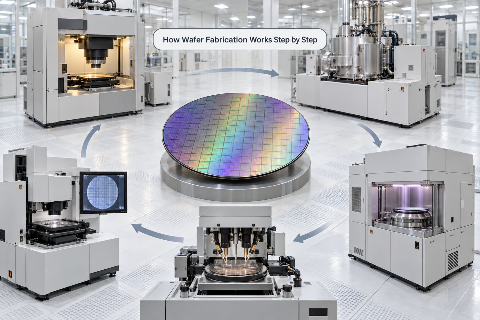
The complete production sequence, before any of the detail, is: circuit design, mask and process data release, silicon wafer production, front-end layer building, contact and via formation, interconnect formation, inline inspection, wafer probe, dicing, packaging, final test, shipment. Eleven stages, and every one of them repeats several times over the life of a wafer.
How Wafer Fabrication Works Step by Step
1. Starting With a Circuit Design
Nothing physical exists yet at this stage. Engineers write the chip in register-transfer level (RTL) hardware description, then run it through simulation, formal verification and synthesis. The tools check the design against timing, power and area targets, and register questions on r/Semiconductors and r/chipdesign keep circling back to the same question: where exactly does design stop and manufacturing start?
The answer is a handoff, not a cliff. Once the design passes verification, place-and-route tools assign every standard cell to a physical location and draw the wires between them. The result is a GDSII or OASIS layout database describing rectangles and polygons on dozens of layers, plus a timing and power report the customer signs off on.
Nothing on the layout is final until the process is known. Rules, spacings and densities depend on which fab and which node you pick, and the same design run on a different process will get different results. That is why the foundry, not the designer, owns the process design kit and the final layout sign-off.
2. Creating Masks and Process Documentation
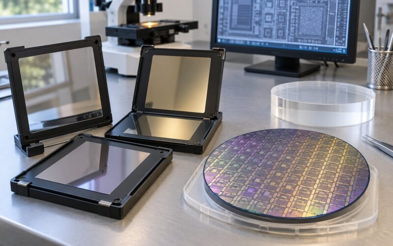
Each drawn layer is rendered onto a photomask, more often called a reticle, made of a quartz plate coated with an opaque absorbing pattern. Modern reticles use extreme ultraviolet (EUV) light at a wavelength of 13.5 nanometres, which lets a single exposure print features that older deep-ultraviolet (DUV) systems needed multiple patterning passes to reach.
A 300 mm reticle set for a leading-edge design can hold a thousand or more distinct masks. Each one arrives with process documentation: a process flow, layer stack definitions, design rules, and the process design kit rules a team must follow to have its layout accepted.
Mask making is one of the slowest, most precise steps in the whole flow. Chrome, EUV-reflective multilayer coatings, and e-beam writing all happen here, and any defect in a mask repeats identically onto every die printed from it, which is exactly what makes a mask defect a wafer-wide problem.
3. Preparing the Semiconductor Wafer
Silicon for wafers starts as quartz sand reduced to metallurgical-grade silicon, roughly 98 to 99 percent pure. That is upgraded by reacting it with trichlorosilane and distilling repeatedly until the polysilicon reaches electronic-grade purity of 99.9999999 percent, often written 9N or 11N depending on the failure digits counted.
The purified polysilicon is melted, and a small seed crystal is dipped into the melt. As the seed is slowly pulled and rotated, silicon freezes onto it in a single crystal called a boule, using the Czochralski method, which melts at about 1,414 degrees Celsius. A minority of applications, mainly power and high-voltage devices, use the floating zone method instead, where a coil of molten silicon moves along a rod and no crucible touches the crystal, giving lower oxygen content.
The boule is then sliced with a diamond-coated saw, lapped to correct thickness variation, edge-rounded, etched to remove surface damage, and polished by chemical mechanical polishing (CMP) into a mirror finish. Shin-Etsu and SUMCO are the two largest silicon wafer suppliers. Each finished wafer carries a notch or orientation flat so the fab equipment can find its orientation, and gets loaded into a sealed pod called a FOUP for transport.
4. Depositing Thin Film Materials
With a clean wafer in hand, the fab starts growing and laying down films. Deposition is how you get conductors, insulators and semiconductor layers onto the surface in a controlled thickness, and the three main methods behave very differently.
| Method | How it works | Strength | Limit |
|---|---|---|---|
| PVD (physical vapor deposition) | Atoms knocked off a target by a plasma or by evaporation | Fast and simple | Poor coverage in deep trenches; line-of-sight |
| CVD (chemical vapor deposition) | Vapour reacts on the wafer to form a solid film | High quality, good step coverage | Higher temperatures |
| ALD (atomic layer deposition) | Sequential self-limiting gas pulses, one atomic layer at a time | Thickness control down to fractions of a nanometre, conformal | Slowest of the three |
Thermal oxidation is a special case: exposing silicon to steam or oxygen at high temperature grows silicon dioxide directly on the surface, which gives a very clean interface. That oxide becomes field isolation, gate insulation in older processes, and the lining between copper and silicon in modern interconnects.
5. Patterning With Photolithography
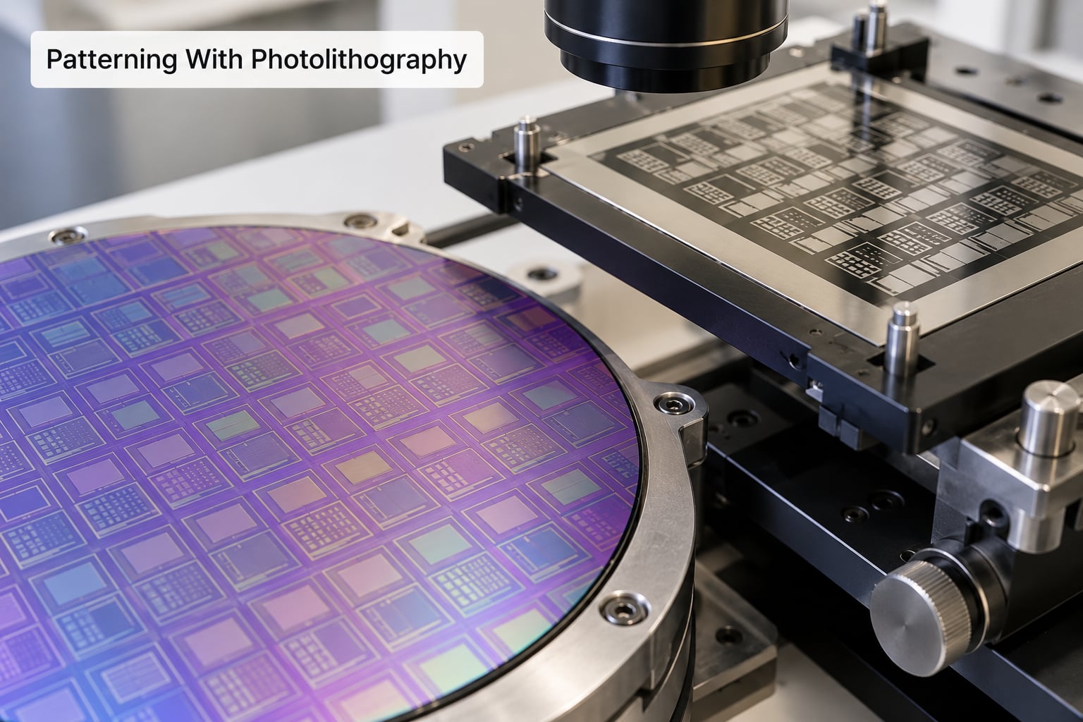
Photolithography is the step that prints the circuit, and it works like a photographic print at a scale where a bacterium would be a stadium. The wafer gets sprayed with photoresist, a light-sensitive polymer, spun on a coater to an even thickness, and soft-baked to drive off solvent. The wafer is then loaded into a scanner, aligned to marks on previous layers, and exposed through the reticle.
Alignment is the hard part. The stepper or scanner matches the new pattern to the last one and holds overlay error to a few nanometres, which is a meaningful fraction of the smallest feature being printed. A stepper prints one field at a time; a scanner scans a narrow slit across the wafer, which is faster and is what leading-edge fabs use with EUV.
After exposure comes a post-exposure bake, which lets the chemistry finish reacting, then development, which dissolves the exposed resist into a developer solution. What is left is a stencil of resist standing on the silicon, and the wafer is hard-baked so the stencil survives the next harsh step. The whole sub-sequence, coat, bake, align, expose, bake, develop, is the heart of how wafer fabrication works step by step.
6. Etching and Transferring the Pattern
The resist stencil is a mask for subtractive work. Where the resist stands, material is protected; everywhere else, it gets removed. Wet etching uses a liquid chemical such as hot alkaline solution and is cheap, fast and highly selective but attacks sideways, so it rounds corners. Dry etching uses a plasma, often in a reactive ion etch (RIE) chamber, where ions are accelerated at the wafer and react chemically with the exposed film.
Dry etch is far more directional, which is why every fine feature in a modern chip is cut this way. The trade-off is selectivity, the ratio of etch rate to the layer you are trying to protect. Too low and the resist or the layer underneath is consumed; too high and the profile stops being vertical. Engineers tune gas chemistry, pressure, and bias power to land in the right place.
Lift-off is the alternative pattern transfer for some interconnect steps: deposit a film over a resist stencil, then dissolve the resist and take the unwanted film with it. Metal stacks are formed with a barrier and liner underneath, because copper diffuses into silicon and poisons devices.
7. Repeating Layers to Build the Circuit
One deposition, lithography, etch, implant, anneal, polish and clean sequence does not produce a chip. It produces one small feature, and the cycle is repeated until a leading-edge design has run through many hundreds of them. Readers on forums are routinely surprised by this number, so it is worth saying plainly: a modern processor line can repeat the core sequence hundreds of times on the same wafer.
Ion implantation is part of each pass. The wafer is exposed to a beam of dopant ions, typically boron for p-type regions and phosphorus or arsenic for n-type regions, and the ions are driven into the silicon to change its electrical behaviour. A thermal anneal afterwards repairs the crystal damage the implantation caused and activates the dopants, so they sit on proper lattice sites and actually conduct.
Oxidation, deposition and CMP fill in between. CMP flattens the surface after patterning so the next lithography pass has something flat to print on, using a slurry and a rotating pad, and the whole surface is cleaned between steps because a single stray particle can kill a whole die.
8. Adding Contacts, Interconnects, and Final Layers
Once the transistors are formed, the MOL stage connects them locally. Contacts land on the source and drain terminals, and vias stack vertically between metal layers. Tungsten is common for the first contact because it forms a clean, low-resistance junction with heavily doped silicon, with cobalt or ruthenium used to reduce resistance further.
The BEOL stage then builds the horizontal wiring. Earlier nodes used aluminium, which became a reliability problem as resistance mattered more, so copper has been standard since the early 2000s. Copper cannot simply be deposited and etched like aluminium, because there is no practical dry etch for copper, so the damascene process fills a patterned trench in a dielectric, then polishes the excess away with CMP.
Between the metal layers sit low-k dielectrics, materials chosen because their dielectric constant is lower than silicon dioxide, which cuts the capacitance loading between wires and lets the circuit run faster and use less power. At the very top, a passivation layer seals the device, and openings are cut in it for the bond pads or the copper pillars that connect the die to the outside world.
9. Inspecting the Wafer During Processing
Nobody waits until the end to check a wafer, because a defect that appears in layer three is still present in layer ninety. Inline inspection runs continuously. Optical inspection tools scan the whole surface for particles and defects, and flag particle counts in the range of a handful per square centimetre. Critical dimension scanning electron microscopy measures the width of printed features on real product structures, and overlay metrology measures how well each layer lines up with the one below it.
These tools feed a process control system that adjusts the next lot. If overlay drifts, the scanner is re-calibrated. If feature widths shrink, the dose or the develop time is changed. A process that cannot hold a control inside a narrow window produces chips that fail electrical test, so this feedback loop is what separates a working line from a batch of scrap.
10. Testing Wafers and Individual Chips
Wafer probe is the first electrical test. A wafer prober steps a probe card onto the wafer, and thousands of microscopic needles make contact with the bond pads of each die in turn. The test equipment runs a sequence of measurements through a test key that reaches the transistors, checks speed, leakage, memory arrays, and analog blocks, and writes a pass or fail result for every die.
Parametric test measures device-level behaviour on selected structures, which engineers track over time to spot drift before it becomes a yield problem. Functional test runs the circuit itself. The output of this stage is a map, and it tells the assembly line exactly which dies are good, which are marginal, and which are dead.
11. Dicing, Packaging, and Shipping the Chips
A finished wafer looks nothing like a retail chip. The wafer is thinned from the back with grinding to a few hundred micrometres, sometimes far thinner for stacked products, and then diced. A diamond blade cuts along scribe lines, or a laser cuts a groove that the wafer snaps along. Individual dies are picked from the dicing tape and sorted.
Packaging puts each die in a carrier. Wire bonding attaches very fine gold or copper wires from the die pads to the package leads, which is still common for cost-sensitive parts, while flip-chip places the die face down and solders directly to a substrate, which shortens the electrical path and is used in nearly all high-performance parts. Advanced packaging pushes further: stacking memory dies on a logic die, adding silicon interposers, and combining several dies into one module, which is how high-bandwidth memory reached terabytes of bandwidth on a single package.
After assembly, the packaged parts go through a burn-in and final test so that early failures are caught before they ship. Then each device gets marked with its part number, lot code and date, and the lot is boxed and sent to the customer, where it is tested once more on the way into the assembly line. It has travelled from a quartz crucible, through a cleanroom, through a probe map, to a sealed package, and almost none of that is visible from the outside.
What Are the Main Wafer Fabrication Process Types?
The flow looks the same from a distance, but the recipes differ substantially. A foundry runs many different process types on shared tools, and the process type determines what the chip is good at.
| Process type | How it is built | Strength | Typical use |
|---|---|---|---|
| CMOS | Complementary MOS pairs, n-channel and p-channel transistors sharing a substrate | Highest density, lowest power, lowest cost per function | Processors, GPUs, mobile SoCs, image sensors |
| Bipolar | Junction transistors with emitter, base and collector | Very high gain, very fast, but high power | Analog and RF mixed signal, some power devices |
| BiCMOS | Bipolar and CMOS on the same die, with an isolation structure between them | Logic density plus analog accuracy | Mixed-signal parts, analog-to-digital converters |
| BCD (bipolar-CMOS-DMOS) | Three device families integrated on one chip | Logic, analog and power switches together | Power management ICs, audio amplifiers, automotive electronics |
| SOI (silicon on insulator) | Thin silicon device layer on an insulating buried oxide | Lower leakage, lower capacitance, better speed per watt | RF switches, image sensors, high-end and photonics parts |
| Compound semiconductor | Materials such as gallium arsenide, indium phosphide, silicon carbide or gallium nitride | High breakdown voltage, direct bandgap light emission, high electron mobility | Optics, lasers, power conversion, radar, RF |
| Memory | Optimised for dense repeating cells, vertical stacking in 3D NAND | Cheapest storage per bit | DRAM, NAND flash |
Leading-edge logic and the newest memory processes are the hardest to run. Since the 22 nanometre era, logic has moved from planar transistors to FinFET, a fin of silicon wrapped by the gate on three sides, and then to gate-all-around, where the gate surrounds the channel on all four. Each of those changes demanded new deposition and etch steps that older process design kits never needed.
Why Does Wafer Fabrication Take So Long?
A wafer spends roughly 12 to 16 weeks inside a fab from start to finished. Most of that is not processing time; it is waiting, cleaning, measuring, and repeating. A single layer touches a dozen pieces of equipment, and each tool is shared among many layers across many recipes, so a lot moves through a queue between steps rather than sitting in a chamber.
The reasons stack up quickly. Layer count is the biggest one: more layers means more opportunities for a defect and more machine passes. Cleanroom conditions are slow by design. The cleanest fab areas run to ISO Class 3, meaning no more than about 100 particles per cubic metre larger than 0.1 micrometres, which is why workers wear full bunny suits and everything arrives through an air shower. Yield takes the third slot, because foundries spend early effort improving yield rather than producing saleable parts, and equipment uptime keeps the fourth, since one lithography scanner or one etcher failing stops every recipe that depends on it.
Wafers themselves add a constraint. Bigger wafers hold more dies, so a 300 mm wafer can yield more good chips per pass than 200 mm, but a defect anywhere on that larger area can take out a bigger absolute number of dies. Different fabs, node generations and product mixes each add their own layer counts, so the real cycle time for a specific part can only be quoted by the foundry making it.
What Happens If a Wafer Defect Is Found?
Detection comes from inline inspection, the test key, and the wafer probe map. The response depends on how the defect behaves. Random defects, usually a particle that killed one die, are removed by the wafer probe map since that die simply fails test. Systemic defects, the same shape in the same place across many dies, point at the process or the mask, and those are the ones that get attention.
A systemic excursion triggers a lot hold. The affected wafers are quarantined, the process engineers pull the excursion wafers, compare them against good and reference wafers, and run root-cause analysis, which usually ends at a specific tool parameter, a photoresist batch, a slurry change or a mask defect. Corrective action can be as simple as adjusting a dose or replacing a seal. If a mask is the culprit, wafers processed with it are scrapped, because the defect prints identically every time.
Rework is possible in a narrow band of cases. A small residue or a minor film defect can sometimes be cleaned and redeposited, or a thin resist layer can be stripped and re-patterned. Anything that removes material permanently is gone, so most excursions are not recoverable and the wafers are scrapped.
That is where yield turns into economics. Cost per good die equals total wafer cost divided by good dies per wafer. A defect density of 0.1 defects per square centimetre sounds negligible, but on a 300 mm wafer covering roughly 706 square centimetres it means dozens of kills, and a denser one at 1.0 per square centimetre would put that into the hundreds. Foundries spend enormous effort on defect detection and prevention precisely because yield is the number that decides whether a process is worth running at all.
Frequently Asked Questions
What are the steps involved in wafer fabrication?
The main steps are circuit design, mask and reticle creation, silicon wafer production, deposition of thin films, photolithography, etching, ion implantation, chemical mechanical polishing, wafer probe, dicing, packaging and final test. The middle six of those repeat many times, because each pass adds one layer of the circuit before the wafer is tested and cut into individual chips.
How many dies fit on a silicon wafer?
It depends on wafer diameter and die area. A 300 mm wafer has about 70,686 square millimetres of surface. Divide that by the die area, then multiply by an edge-exclusion factor of roughly 80 to 90 percent to allow for the unusable rim and the space between dies. A 100 square millimetre die therefore yields roughly 565 to 636 potential dies, of which 85 percent or so normally pass final test.
Who is the largest manufacturer of silicon wafers?
Shin-Etsu and SUMCO together supply most of the world’s semiconductor silicon wafers, and Shin-Etsu has held the leading position for years. German Siltronic is the next largest supplier. Wafer production is a separate business from chip fabrication: these companies grow, slice and polish the blanks, then sell them to foundries.
How long does wafer fabrication take?
A wafer spends roughly 12 to 16 weeks moving through a fab, and that figure includes waiting time between tools, not just processing. Actual processing per layer is minutes to hours, but each of the hundred-plus layers requires several machine passes plus inspection. Advanced nodes run longer than mature ones, and cycle time is not something a customer can shorten on their own.
Why do semiconductor fabs need cleanrooms?
A modern transistor features are measured in nanometres, and a single dust particle landing on a die can break a circuit or short two wires. Fabs run at ISO Class 1 to Class 3 cleanliness, with HEPA and ULPA filtration, positive pressure, full bunny suits for operators, and air showers for anyone entering. A modern process density is so high that ordinary dust would destroy most of the output.
Can I make my own semiconductor?
Not a modern chip, not from your garage. A leading-edge fab costs billions of dollars and needs thousands of specialists, and each wafer of a 2 nanometre design runs into thousands of dollars. The realistic routes are an FPGA or ASIC shuttle run through a foundry service, older and much larger node processes used for MEMS and sensors, or a university cleanroom, which teaches the flow without needing a commercial line.
Conclusion: Start With the Complete Manufacturing Flow
The whole story fits in one sentence: pure silicon is grown into a single crystal, sliced and polished into a wafer, then printed with layers again and again, where each layer is deposited, patterned with light through a mask, etched, doped and polished, until the wafer is probed, cut up and sealed into packages.
Learn that sequence first and the acronyms stop being a wall. Once FEOL, MOL and BEOL have a place in the order, terms like CMP, ALD and damascene have somewhere to attach. After that, go deep on the single module you care about, because process engineers spend whole careers inside one of those steps rather than across all of them.