A chip process node is a name for a foundry’s manufacturing process, and for most of the last two decades that name has been a marketing label rather than a physical measurement. A 7nm process does not contain any feature that measures seven nanometers, and a 3nm chip is not built with lithography light three nanometers wide. Understanding how chip process nodes are named means separating three things that the name now blends together: which era the label came from, which foundry invented it, and what the process actually delivers on a die.
The naming convention did real work once. Early node numbers tracked the gate length of a transistor, and later ones tracked a half-pitch figure pulled from roadmaps. Since the 45nm generation, and especially since finFETs arrived around 22nm, the number has drifted away from any dimension you could measure with a microscope. It survives because it works as a generational marker that roughly tracks density and power improvements, not because it describes the silicon.
Three eras explain almost everything:
- Gate length era: the number was the transistor gate length, and early nodes like 180nm, 130nm, and 90nm were close to literal.
- Half-pitch era: industry roadmaps started naming nodes after half the dense memory cell pitch, which is a contactable feature but not a transistor dimension.
- Label era: each foundry picks its own reference point and its own cadence, so the number became a generation name attached to a specific design rule set.
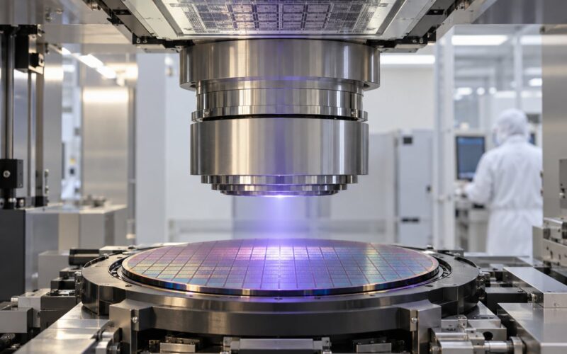
One more confusion deserves clearing up before we go further. When a foundry says it uses 193nm ArF immersion lithography, that 193nm is the wavelength of the light source. It has nothing to do with the 7nm node name printed on the same chip. Tool wavelength, minimum feature size, and node name are three separate numbers that people routinely mix up.
Table of Contents
- Process Node Names at a Glance
- How Chip Process Nodes Are Named and Why They Are Misleading
- Why Semiconductor Companies Originally Used Physical Dimensions
- How the 10 nm, 7 nm, 5 nm, and 3 nm Labels Evolved
- What Does a 3 nm or 2 nm Process Node Actually Tell You?
- Which Specifications Are More Useful Than the Node Name?
- Why Are Chips with Smaller Nodes Not Always Faster or More Efficient?
- How to Compare Two Process Nodes Without Falling for the Label
- Frequently Asked Questions
- Are smaller process nodes always faster, smaller, or more power-efficient?
- Why can a chip labeled 3 nm use more power than one labeled 5 nm?
- Are process node numbers from different foundries directly comparable?
- Does a 2 nm process mean every transistor feature measures two nanometers?
- How should engineers choose between two differently labeled process nodes?
- Conclusion: Read the Metrics Behind the Name
Process Node Names at a Glance
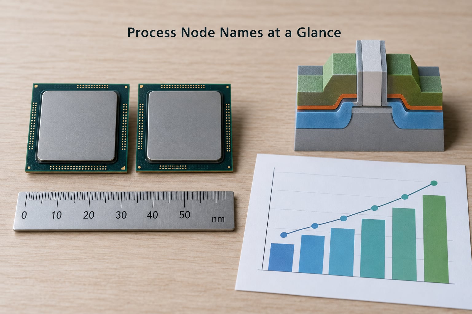
The table below is the shortest useful answer to the naming question. It separates what a node label literally uses, what it originally referred to, what it signals now, and what you should measure instead.
| Node label | Literal unit | Original basis | What it signals today | What to measure instead |
|---|---|---|---|---|
| 90nm, 65nm | Nanometres | Approximate gate length | A generation, roughly | Gate length, metal pitch |
| 45nm, 32nm | Nanometres | Gate length, then half-pitch | The last nodes with a physical referent | Gate pitch, SRAM cell size |
| 22nm, 16nm, 14nm | Nanometres | Foundry-specific reference dimension | A design rule generation | Metal pitch, contacted poly pitch |
| 10nm, 7nm, 5nm, 3nm | Nanometres | Marketed cadence | A foundry’s own ladder of generations | Transistor density, performance per watt |
| Intel 7, 4, 3 | No unit | Competitive positioning label | Which Intel generation a chip uses | Density, frequency, watts per core |
| TSMC N3, N2, A16 | No unit | TSMC internal generation code | A specific TSMC process variant | SRAM cell size, design rules, yield maturity |
| Intel 18A, 14A | Angstroms | Nanometres written in angstroms | The first post-nanometre naming step | Density, backside power delivery, RibbonFET |
| Samsung 1c, 2c, 3c | No unit | Second, third, fourth generation | A generation within an nm label | Transistor structure, density |
How Chip Process Nodes Are Named and Why They Are Misleading
Most modern node numbers began as approximate feature-size or gate-length labels, and today they work primarily as generation and market-position names. The direct reason they mislead is that every foundry chooses its own reference dimension and no two foundries choose the same one. The suffix letters, vendor prefixes, and process variants are not standardised either, so N2, Intel 4, and 2nm are three separate naming systems rather than three entries in one scale.
The suffix letters are where most readers get lost. TSMC appends letters to mark performance and power variants of the same generation: N3P is the higher-performance N3, N3E is the enhanced version built for efficiency, and A16 sits in the same family with backside power delivery. Samsung uses a letter for generation, so 1c is the second-generation 1nm process and 3c is the fourth-generation 3nm process. Intel simply dropped the unit and writes Intel 7, Intel 4, and Intel 3. None of these suffixes means a physical dimension, and none of them is comparable across vendors.
That last point is worth sitting with, because it is the root of almost every argument in the comments sections. The engineer’s consensus, well established in chip design forums, is blunt about it: node numbers are marketing numbers, and only shipped silicon tells the truth. Practitioners reach that conclusion from the practical direction, treating design rule check values and pitch measurements as ground truth rather than node names. Meanwhile the dominant view in enthusiast communities is that industry professionals already ignore the labels and outsiders keep reading them literally, which is a fair summary of why the confusion persists.
Why Semiconductor Companies Originally Used Physical Dimensions
Physical dimensions were the original basis because early transistors were simple enough that one number described the whole device. A gate length of 100 nanometres was the single most important constraint, and printing a larger number on the process sheet told a designer what the transistor could switch and how fast it would respond. As long as the number came straight off the mask geometry, the label was honest.
The industry then moved to the half-pitch definition published through the International Technology Roadmap for Semiconductors. Under that rule, a node name is half the pitch of a dense memory cell array, which is a real, contactable manufacturing feature. The trouble is that a half-pitch is not a transistor gate. In practice, the gate had already shrunk below the value implied by the label, and companies kept reusing the number across process generations so that “16nm” and “14nm” would sound like steps in the same ladder.
The result was a system that measured the roadmap rather than the chip. As long as everyone used the same half-pitch reference, the names lined up and comparisons worked, even though nobody reading a 7nm datasheet could find a 7nm feature on the die.
What broke the system was physical, not editorial. Around 22nm, planar transistors hit leakage and power walls, and the answer was a finFET: a three-dimensional channel wrapped around a thin fin. That change altered device physics and design rules completely, and it meant front-end-of-line and back-end-of-line features no longer shrank in step with each other. Interconnect layers could no longer follow the transistors down, and wires became the limiting factor long before gate lengths ran out.
How the 10 nm, 7 nm, 5 nm, and 3 nm Labels Evolved
By the 10nm generation, node names had become product names for design rule sets. The table below shows what each numeric style originally referred to and what it now communicates, with a caution that these are not performance claims.
| Naming style | What the number originally represented | What it communicates now | Examples |
|---|---|---|---|
| Gate length | Approximate transistor gate length | Historical era only | 180nm, 130nm, 90nm |
| ITRS half-pitch | Half the dense memory cell pitch | A rough generational step, loosely used | 45nm, 32nm, 22nm |
| Foundry numeric | Varies by vendor, sometimes a contactable pitch | A marketing cadence, each vendor’s own | TSMC 16nm, 12nm, 7nm, 5nm, 3nm |
| Letter prefix | An internal process code | Identifies the exact process variant | TSMC N3, N3E, N3P, N2, A16 |
| Unnamed generation | Nothing; the unit was dropped on purpose | Competitive positioning | Intel 7, Intel 4, Intel 3 |
| Angstrom | Nanometres expressed in angstroms | Deliberate move below 2nm | Intel 20A, 18A, 14A |
| Generation letter | Which iteration of an nm label | Process generation within a family | Samsung 3c, 2nm, 1c, 2c |
Intel’s history makes the drift visible in a single list. 10nm Enhanced SuperFin, a second-generation 10nm process, was rebadged as Intel 7, and Intel 4 was a genuine 7nm-class EUV node. The 2020s naming then turned to angstroms, with 20A, 18A, and 14A marking a shift below 2nm, and 18A was Intel’s first process in high-volume manufacturing with gate-all-around RibbonFET transistors and backside power delivery. Writing 1.8nm as 18A sidesteps a round-number claim and reads as a different unit on a spec sheet.
TSMC’s system is the clearest to decode. The N prefix is simply TSMC’s marker for its FinFET-derived family, and the number after it is a generation counter, not a measurement: N3, N3E, and N3P share a generation, and N2 is the next one down. A16 is the angstrom-labelled member of that generation with backside power delivery. If a reader asks what the N in TSMC N3 means, the honest answer is that it carries no numeric information at all.
Samsung’s letters count iterations instead. Because Samsung first announced a 1nm node, it needed a way to label later improvements, so it used 1b and then 1c for successive generations. The same logic produced 2c, meaning the third generation of the 2nm family. When a spec sheet lists 3c against an N3, you are comparing a fourth-generation Samsung process with a first-generation TSMC one, and the numbers only line up by coincidence.
The convention is not pure fiction, and it would be unfair to treat it as one. Within a single foundry’s own ladder, a smaller number does usually mean higher density and better performance per watt, because each step is a deliberate process improvement. The problem is cross-vendor comparison, where the numbers mean whatever each vendor’s marketing decided they mean.
What Does a 3 nm or 2 nm Process Node Actually Tell You?
A 3nm or 2nm label reliably tells you three things: which foundry’s process family you are dealing with, roughly when it entered production, and which transistor generation it belongs to. On current roadmaps, TSMC’s N2 entered high-volume manufacturing in late 2025, and Intel’s 18A refers to 1.8 nanometres with gate-all-around transistors and backside power delivery. Those are useful facts, and they are enough to place a chip in a timeline.
What the label cannot tell you is anything measured. It does not give you transistor density, the SRAM bit-cell area, the standard-cell height, the number of metal layers, the power per operation, the achievable frequency, or the die area a given block will occupy. It also does not tell you how mature the process is, and maturity often matters more than the number on the launch slide. A design that is two years past high-volume manufacturing will hit yield far more predictably than a brand-new node ramping on a first tapeout.
Marketing terminology and measurable data are easy to confuse because the terminology feels technical. A 2nm name is a product identifier in exactly the way a car trim level is, and the honest test is simple: if two chips wear the same number from the same vendor, the number tells you they are close relatives. If two chips wear different numbers from different vendors, the number tells you almost nothing on its own.
Which Specifications Are More Useful Than the Node Name?
Density, pitch, and power figures are what engineers actually compare. The table below lists the metrics that carry information, along with what each one captures and where it breaks down. No single row makes one node universally better, which is exactly why the node name is a poor substitute for the whole table.
| Metric | What it measures | Why it matters | Its limitation |
|---|---|---|---|
| Transistor density | Millions of transistors per square millimetre | Directly tracks how much logic fits on a die | Different cell mixes give different totals |
| SRAM bit-cell size | Area per stored bit | Governs cache and L2 size on a given die | SRAM often scales worse than logic |
| Standard-cell density | Cells per unit area | The practical layout number for a design | Foundry-specific cells, not portable |
| Contacted poly pitch | Gate-to-gate spacing at the contact | A front-end-of-line measure the gates actually hit | Not what any node name reports |
| Minimum metal pitch | Back-end-of-line interconnect spacing | Sets wire density and routing headroom | Wires lag gates on every node |
| Transistor type | FinFET, nanosheet, or gate-all-around | Determines leakage behaviour and drive current | No numeric ranking across structures |
| Performance per watt | Work delivered per unit of energy | The number that decides battery life | Highly workload dependent |
| Peak frequency | Clock rate at a stated power | Useful for peaky workloads like rendering | Irrelevant to heavily threaded work |
| Die area per block | Physical area of an IP block | Reveals real-world cost and yield effects | Only known after tapeout |
| Wafer cost and yield maturity | Cost per good die, and process age | Often the deciding factor for a product | Foundry pricing is rarely public |
| Process variation | Timing and leakage spread across a die | Determines how tight designs must be | Hard to compare without measurement data |
The clearest illustration of why density beats the label comes from the numbers Intel published for its own 10nm process, which put transistor density at 100.76 MTr/mm2, against a widely cited 91.2 MTr/mm2 for TSMC’s 7nm. On paper, a larger node number delivered more transistors per square millimetre. The IEEE paper “A Density Metric for Semiconductor Technology,” published in Proceedings of the IEEE, volume 108, number 4, pages 478 to 482, made this argument formal by proposing the Logic, Memory, and Connectivity metric. Intel responded with its own density proposal built on NAND2-style and scan flip-flop cells, and the fact that two credible companies felt the need to publish competing density metrics tells you how far the node label had drifted from measurement.
Why Are Chips with Smaller Nodes Not Always Faster or More Efficient?
A smaller node name changes what a foundry can offer, but it does not decide the finished chip. Architectures differ, voltage targets differ, and the same silicon behaves differently depending on what the designer asks of it. The instinct to assume that how chip process nodes are named and why they are misleading reduces to a simple ranking of numbers is understandable, but the number is an input to that decision rather than the decision itself.
Consider two otherwise comparable designs, one built on a 7nm class process and one on a 5nm class process, both running a single-threaded integer workload. The newer design may fit more logic per area and hold a higher clock, but it can still lose if it runs a higher voltage to do so, or if more of its gain is eaten by cache misses, or if the workload simply does not scale with the extra transistors. On a bandwidth-bound task the result can reverse entirely, because the older process spends more of its budget on memory rather than logic.
Interconnect is the structural reason. Around the 7nm era, wires rather than gates became the binding constraint, and Semiconductor Engineering’s coverage of those pain points described the situation plainly: front-end and back-end scales no longer matched at any foundry. When wires stop shrinking in step with transistors, a newer node buys you transistors you cannot cheaply feed, and the theoretical density gain evaporates in routing congestion and added power.
Thermal limits, memory hierarchy, and process variation add their own noise. Power density that a server part tolerates is a problem in a phone, and tighter variation across a die forces designers into more guardband, which costs both power and area. None of that shows up in the node label, and all of it shows up in a benchmark.
How to Compare Two Process Nodes Without Falling for the Label
There is a workable method, and it takes about an hour once you know where to look. It works for a fabless team choosing between foundry options and just as well for a student trying to read a spec sheet.
1. Fix what you are comparing. Write down the metric before you start. If the question is which node makes a smaller die for a given block, you need area data. If it is which runs cooler, you need watts per operation, and the node name contributes nothing.
2. Compare like for like. Density figures are only meaningful against the same cell definition. Mixing a foundry’s high-density logic number with a competitor’s conservative number flatters whoever is more aggressive, and the difference can be large enough to reverse a ranking.
3. Run the same workload. Performance per watt and effective frequency are workload specific. Use a benchmark resembling the application, and treat a vendor’s own claims as claims until a third party reproduces them.
4. Weight maturity heavily. A process that has been in high-volume manufacturing for two or three years will yield better than a node one generation ahead but barely ramped. Design cost, mask cost, and the risk of a respin all move with maturity, and for most products that trade is worth taking.
5. Read the design kit, not the roadmap. Process design kits publish contacted poly pitch, minimum metal pitch, SRAM cell dimensions, and standard-cell libraries. Those numbers are what an IP block will actually be built from, and they are the closest thing to ground truth available outside the foundry.
6. Check cost per transistor, not cost per wafer. A more expensive wafer on a denser process can still produce a cheaper function, and the crossover point moves as yields mature. This is where the absence of a pricing convention hurts readers most, since per-transistor economics are the argument node names were supposed to support and cannot be checked from public data.
Once you have done that, the node name is still useful as a shorthand for where a part sits in its vendor’s roadmap. Keep it as shorthand and stop treating it as a measurement.
Frequently Asked Questions
Are smaller process nodes always faster, smaller, or more power-efficient?
No. A smaller number usually signals a newer process within one vendor’s own ladder, and newer processes tend to offer higher density and better performance per watt. But a finished chip also depends on architecture, voltage targets, cooling, memory design, and workload. Two chips with different node numbers from different foundries can perform almost identically, and the newer one can draw more power if it runs at a higher clock.
Why can a chip labeled 3 nm use more power than one labeled 5 nm?
Because the label says nothing about power. Designers set voltage and frequency targets, and a 3nm part running at a higher clock or higher voltage will draw more power than a 5nm part running conservatively, even if the smaller process could do better. Workload matters just as much: a heavily threaded server chip on a newer node can out-consume an efficiency-tuned part on an older one for identical work.
Are process node numbers from different foundries directly comparable?
Not reliably. Each foundry picks its own reference dimension, and none is standardised across the industry. TSMC 7nm, Intel 7, and Samsung 7nm are unrelated labels. The closest available comparison is transistor density measured against the same cell definition, which is why Intel 10nm at 100.76 MTr/mm2 could out-density a competing 7nm process at 91.2 MTr/mm2.
Does a 2 nm process mean every transistor feature measures two nanometers?
No. Nothing on a 2nm die measures two nanometers. Gate length, contacted poly pitch, and minimum metal pitch are all larger, and the interconnect pitch is larger still. The number is a generation name tied to a design rule set. Reading it as a physical dimension leads directly to the wrong conclusion about die size, cost, and what a foundry can actually build.
How should engineers choose between two differently labeled process nodes?
Start from the metric your product is judged on, then compare like for like. Use transistor density with the same cell definition, read contacted poly pitch, minimum metal pitch, and SRAM cell size from the design kits, and test performance per watt on a workload that matches the application. Weight maturity heavily, since a mature node usually yields better than a barely ramped one, and check the total cost per delivered function.
Conclusion: Read the Metrics Behind the Name
Process node names are useful shorthand, and in 2026 they still tell you which generation and which foundry a chip came from. They are not physical measurements, and treating them that way produces the wrong answer about size, power, and cost more often than not. Start with one move: pick the metric your decision actually turns on, then go find that number from design kits, published density figures, or independent measurements on the same workload, and ignore the name on the way.