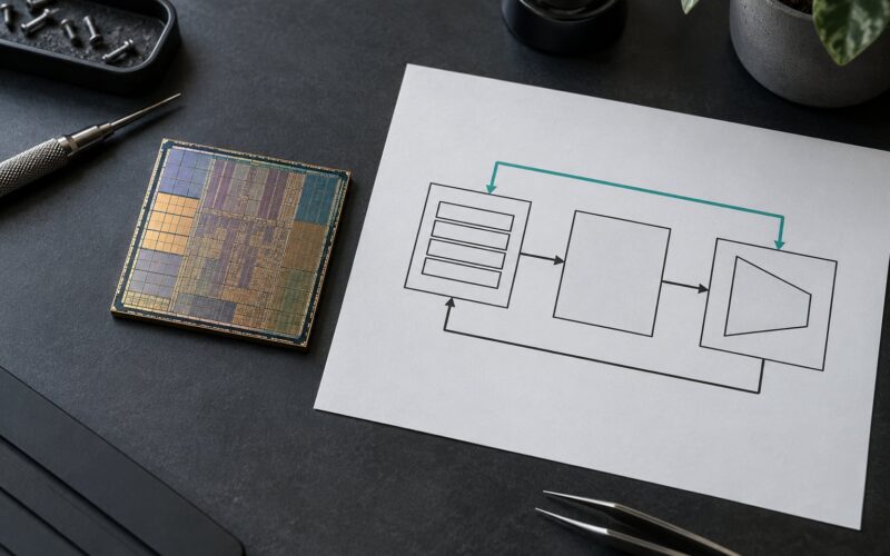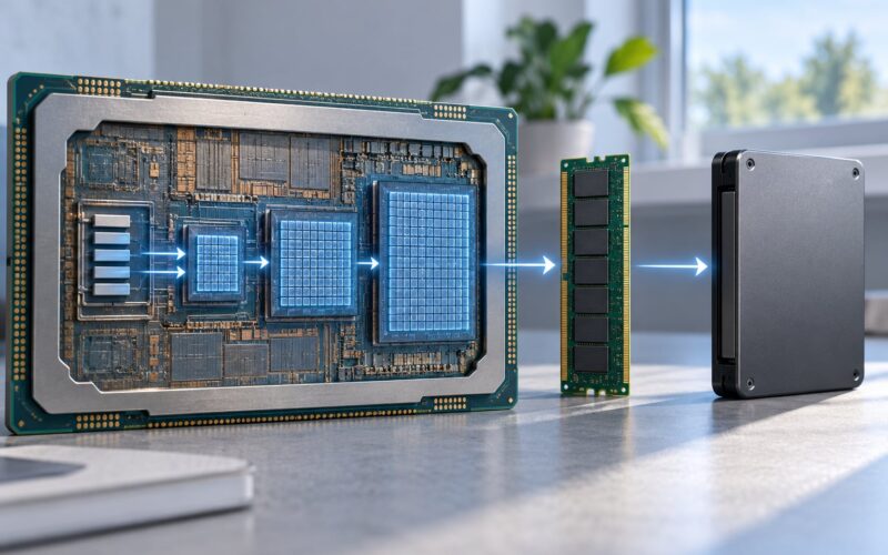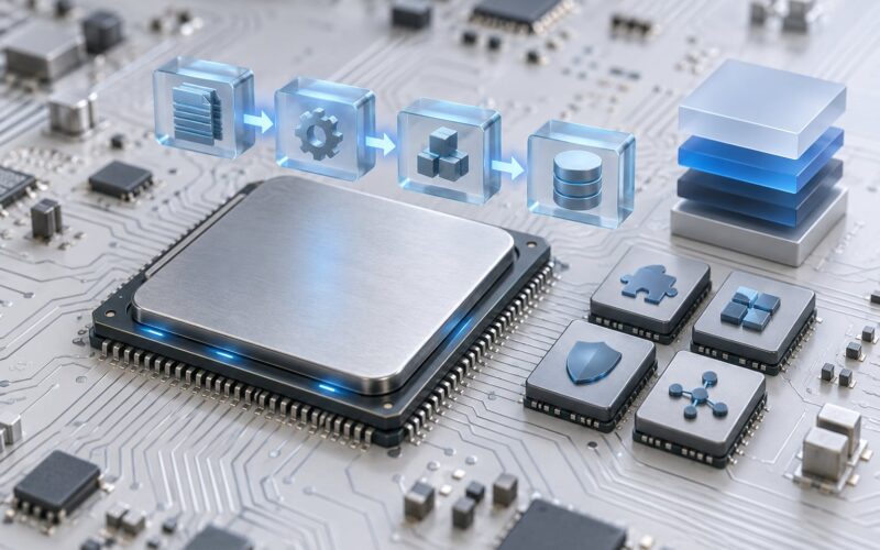
A tensor core is a specialised execution unit built into a chip that performs matrix multiply-accumulate — written as D = A x B + C — on a whole small tile of operands in a single instruction, at many times the throughput of a general-purpose core for that one operation. A matrix unit is the hardware designer term for the same idea, and the two words describe slightly different emphases. This guide covers how the hardware works, how the architectures differ across vendors, and what the constraints are that decide whether a real kernel gets any of the speed on paper.
Table of Contents
- How Tensor Cores and Matrix Units Handle AI Workloads
- What Is a Tensor Core?
- Tensor cores and matrix units explained in one instruction
- What Is a Matrix Unit?
- Tensor Cores vs. Matrix Units: What Changes?
- How Matrix Multiplication Becomes Hardware Work
- How Do Tensor Cores and Matrix Units Improve AI Performance?
- Where Are They Used in GPUs, NPUs, and Other Chips?
- Precision, Data Types, and Accuracy Tradeoffs
- How to Choose the Right Hardware for an AI Workload
- Tensor Cores and Matrix Units Explained: Key Takeaways
- Frequently Asked Questions
- Can you explain what tensor cores are and how they work?
- What is a tensor matrix?
- What are the key differences between CUDA cores and tensor cores?
- Do tensor cores accelerate FP32?
- How is matrix multiplication done on a GPU?
- Does using FP16 automatically activate tensor cores?
How Tensor Cores and Matrix Units Handle AI Workloads
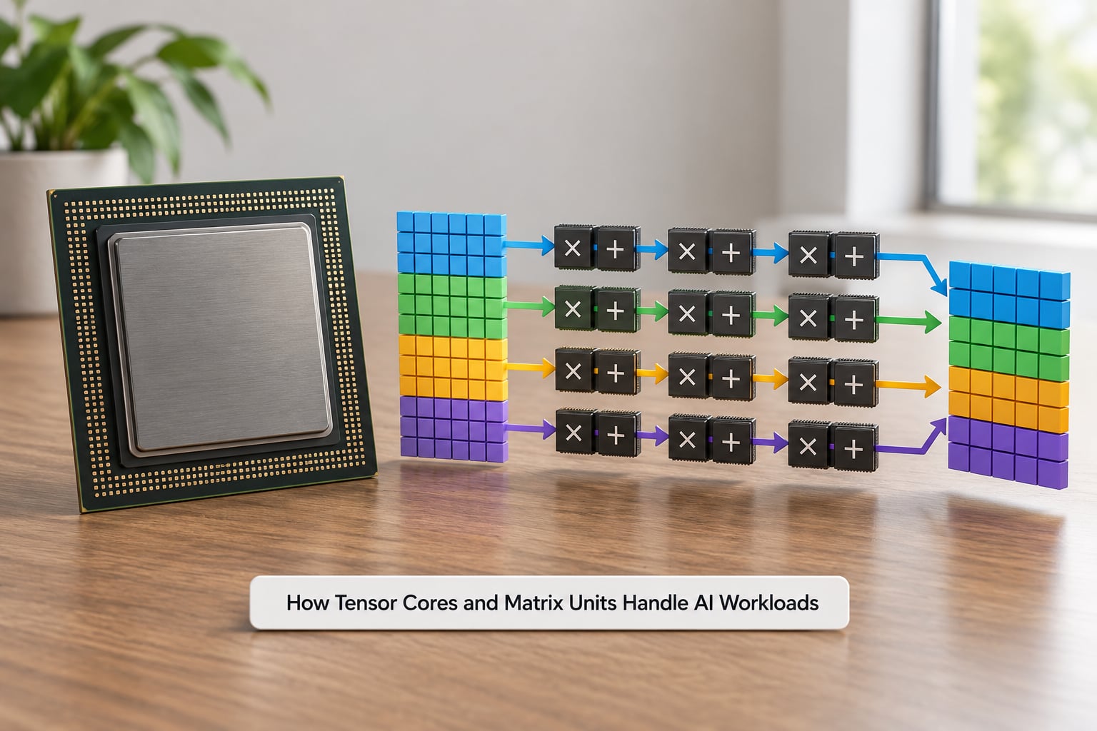
Almost every arithmetic-heavy layer in a modern neural network reduces to the same primitive: multiply two matrices together. Attention projections, feed-forward layers, the batched matrix operations in a decoder, the convolution turned into an im2col GEMM — all of it ends up as dense matrix multiplication, usually called GEMM after the BLAS routine that does it.
That is the entire reason matrix hardware exists. A general-purpose core executes one instruction per thread per clock and spends most of its energy on instruction decode, register movement and address arithmetic. A matrix unit throws all of that away: it fetches two fragments into registers, runs a fixed grid of multipliers over them, and writes back a tile of results. Nothing else happens in the datapath.
The payoff shows up in two very different places depending on the workload. In training, and in the prefill phase of inference where a whole prompt is processed at once, you are doing arithmetic intensity and compute is the bottleneck. The matrix unit is the bottleneck resource, so widening it moves the wall clock time.
In the decode phase of inference, where the model emits one token at a time, you are reading a model’s worth of weights out of memory for a handful of matrix operations. There, memory bandwidth sets the pace and the matrix unit is mostly idle. Batching requests is what pushes decode back toward compute-bound, which is why the same chip behaves so differently under a busy serving load than a one-off benchmark.
Everything else these units touch — convolutions, sparse matrix multiply, FFT and Hadamard transforms, prefix scans, reductions, dynamic programming — is either GEMM in disguise or a reduction that a fixed-size array happens to do well.
What Is a Tensor Core?
A tensor core is a fixed-function unit that computes one small matrix multiply-accumulate per instruction, cooperatively across a group of threads. The three operands have fixed roles: A and B are the input fragments, C is the accumulator read in and added, D is the result written out.
Tensor cores and matrix units explained in one instruction
On NVIDIA hardware the instruction names the whole geometry, for example mma.sync.aligned.m16n16k16.row.col.f32.f16.f16.f32. Read that as: synchronous, warp-collective, 16 rows by 16 columns of output accumulated over a depth of 16, with FP16 inputs and an FP32 accumulator. Ampere added 8×8 forms, Hopper introduced larger warp-group forms such as wgmma that are issued by a group of warps rather than one.
Nothing about that instruction is negotiable at run time. The tile shape is baked into the silicon, which is why matrix dimensions need to be multiples of 8 or 16 for the fast path, and why a matrix that does not fill the array wastes hardware.
The vocabulary trips people up more than the hardware does, so it is worth one short detour. A tensor is just a labelled array of numbers. A matrix is a rank-2 tensor, a vector a rank-1 tensor. When a neural network layer computes Y = XW, it is contracting a tensor dimension — multiplying and summing across the shared axis. “What is a tensor matrix” usually means exactly this: the object a tensor core consumes is a plain matrix or a stack of them, and a “tensor matrix” as a separate type of thing does not exist.
| Aspect | Tensor core (NVIDIA naming) | CUDA / shader core |
|---|---|---|
| Unit type | Fixed-function matrix datapath | General-purpose vector pipeline |
| Operation | Matrix multiply-accumulate on a fixed tile | Any scalar or vector instruction |
| Data types | FP16, BF16, TF32, FP8, FP4, INT8, INT4 | FP32, FP64, INT32, and the same narrow formats |
| Parallelism | One warp-collective or warp-group instruction | One thread per instruction |
| Control flow | Fixed sequence, no branches inside a tile | Full branch, call and predicate support |
| Programmer view | Through WMMA, mma.sync, or high-level libraries | Direct, instruction by instruction |
| Best fit | Dense and structured-sparse GEMM | Everything else, plus small or oddly shaped math |
One recurring misconception deserves a line of its own. Tensor cores do accelerate FP32 work — through the TF32 path, which keeps a 10-bit mantissa inside a 32-bit format, and through any of the narrow formats cuBLAS and CUTLASS will hand you. A plain IEEE FP32 GEMM does not run on the tensor path at all, so the honest answer is “yes, with a different number format, and you have to ask for it”.
What Is a Matrix Unit?
A matrix unit is a block of silicon whose only job is multiplying and adding matrix elements. Where “tensor core” names the product feature, “matrix unit” names the design object, and it is how an architect describes the block on a block diagram.
The defining implementation choice is the systolic array. Instead of pulling every operand out of memory for every single multiply, you stream A rows in from one edge and B columns in from the top, and each partial product hops one grid cell per clock until it lands in the accumulator register file at the far corner. The rhythm of the data movement is what keeps the multipliers fed.
That dataflow has a real design payoff. Each operand is fetched once and reused across the whole array, so arithmetic intensity inside the block is high by construction and the array needs far less register file bandwidth than a traditional design. The cost is rigidity: fixed dataflow, fixed tile shape, and a hard requirement that dimensions align.
Register blocking is the companion technique. Each thread or warp holds a small patch of C in registers and loops over K, reloading a fresh A fragment and B fragment per step. Get the blocking right and the tensor path runs near its peak; get it wrong and you stall on operand fetch, which is the single most common reason a kernel issues tensor instructions and still runs at a fraction of the advertised rate.
For a design team, a matrix unit is also an IP decision. A hard macro gives you a proven array, a datapath and a verified model, but a fixed geometry and a vendor-tied interface. A soft IP version lets you set tile shape, precision mix and register width yourself, at the cost of the verification work. Most teams buying a matrix unit today are picking between those two, and the tile geometry they are stuck with for a product’s lifetime is the most expensive thing on the datasheet.
Tensor Cores vs. Matrix Units: What Changes?
Mostly the emphasis and the control model, not the physics. Both are matrix multiply-accumulate engines, and no implementation on the market is identical to any other. The differences that matter to a designer fall into a handful of buckets.
Terminology. “Tensor core” is NVIDIA’s brand for a feature and is now used loosely. AMD says Matrix Core, Google says MXU, Apple and Intel say AMX, FPGA vendors say DSP block. Underneath, all of them multiply matrices in a fixed array.
Granularity of control. NVIDIA’s units are driven by per-instruction fragments of a few dozen elements. Google’s MXU is a large array driven a whole tile at a time by compiled code, and Apple’s and Intel’s AMX are wide tiles loaded explicitly into a dedicated block of registers. The fine-grained model gives more scheduling freedom; the coarse one gives more predictable throughput per cycle and far fewer instructions to issue.
Register file depth. This is the quiet one. How many C elements a unit can hold while it accumulates determines how much of a K loop it can absorb before spilling. Deep accumulator files let a large tile run at full rate; shallow ones force smaller tiles and more memory traffic per FLOP.
Precision menu. A unit built for FP16 only will not accept INT8, and a unit built for INT8 only will not do FP8. Some designs add dedicated sparsity paths, some a second block for fine-grained transforms.
Placement. A GPU tensor core sits beside general-purpose cores and shares the memory hierarchy. An MXU sits next to a vector memory designed to feed it. An AMX block sits beside a CPU. Same operation, completely different surrounding system.
How Matrix Multiplication Becomes Hardware Work
The mapping is easier to see with numbers. Take a small C = A x B where A is 2×2 and B is 2×2: A row 1 is 1, 2; A row 2 is 3, 4. B column 1 is 5, 6; B column 2 is 7, 8.
C[0][0] is 1 times 5 plus 2 times 6, which is 5 plus 12, which is 17. C[0][1] is 1 times 7 plus 2 times 8, which is 7 plus 16, which is 23. C[1][0] is 3 times 5 plus 4 times 6, which is 15 plus 24, which is 39. C[1][1] is 3 times 7 plus 4 times 8, which is 21 plus 32, which is 53.
Four outputs, eight multiplies, four adds, and a loop over K that a general-purpose core would run with each element loaded, multiplied, added and stored individually. On a matrix unit, the A fragment and the B fragment are loaded once, eight partial products are computed in parallel, and the four sums accumulate into the C registers — the D = A x B + C form, in one pass.
Scale that up and the real problem appears. A 4096×4096 by 4096×4096 GEMM is roughly 137 billion multiply-accumulates, and the naive layout reads every input element from memory about 4096 times. A tiled implementation walks K in steps, holds an output tile in registers, and drops total memory traffic by orders of magnitude.
So the hardware sets the rhythm, and the tiling sets the traffic. Neither alone gets you the throughput.
How Do Tensor Cores and Matrix Units Improve AI Performance?
There are five factors, and they interact. Understanding which one is binding tells you why a kernel is or is not fast.
Arithmetic throughput per instruction. One tensor instruction replaces hundreds of scalar multiply-adds, which is where the headline numbers come from. It is also the least useful number on its own.
Memory movement. The roofline model puts a hard ceiling on any kernel: its achievable rate is the lower of the machine’s peak compute and peak memory bandwidth times the kernel’s arithmetic intensity in FLOPs per byte. A GEMM with well-chosen tiles has high arithmetic intensity and runs under the compute roofline. A badly tiled one drops under the bandwidth roofline and no amount of extra tensor throughput helps.
Precision. Halving the bytes per operand cuts memory traffic and often doubles the achievable multiply rate. This is why FP8 and FP4 moved the practical ceiling more than the raw FLOP figures suggest.
Sparsity. Structured 2:4 sparsity, where every group of four consecutive values has two zeros, can double effective throughput because the hardware skips the zero pairs. The requirement is rigid: a dense matrix gets nothing from it, and a lightly pruned one gets nothing either.
Utilisation. Occupancy, shared memory bandwidth, bank conflicts, async pipelining, warp specialisation, alignment and tile shape all decide how much of the hardware you actually keep busy. A GEMM that issues only mma.sync instructions and spends 70% of its time waiting on shared memory loads has a tensor path and no speed.
One more practical note: the “tensor core count” printed on a GPU spec sheet is a per-part number of fixed blocks, not a performance rating. Two chips with the same count differ widely once clock, memory bandwidth, cache size and tile geometry enter the picture, and the number stops predicting anything once clock limits or thermals take over.
Where Are They Used in GPUs, NPUs, and Other Chips?
Every segment that runs dense AI now ships a matrix unit. The name changes, the array geometry changes, and the surrounding system changes more than the core operation does.
| Vendor and part | Unit name | Array or tile shape | Typical precisions | Control model | Reached through |
|---|---|---|---|---|---|
| NVIDIA, Volta onward | Tensor Core | Small per-warp tiles, for example m16n16k16, with larger warp-group tiles on Hopper | FP16, TF32, INT8, then BF16, FP8, FP4 | Warp-collective or warp-group instruction | CUDA via cuBLAS, cuBLASLt, CUTLASS, WMMA, mma.sync, wgmma |
| AMD, RDNA and CDNA | Matrix Core | WMMA-style tiles per workgroup | FP16, BF16, INT8, FP8 on newer parts | Workgroup-level wavefront instruction | ROCm via rocBLAS, HIP |
| Google, TPU | MXU | Large 128×128 systolic array | BF16 primary, INT8 and other formats per generation | Whole-tile operation, no shape duality | XLA, Pallas, TorchTPU |
| Apple, M-series and A-series | AMX | 512-byte tile across a block of registers | INT8 and BF16 | Explicit tile load, then a single wide operation | Core ML, oneDNN, Metal |
| Intel, Xeon and Core | AMX | 512-byte tile, 8 rows x 64 columns of B | INT8 and BF16 | Explicit tile load and execute | oneDNN, Intel Extension for PyTorch |
| FPGA vendors | DSP block or soft matrix IP | Configurable, often 4×4 or smaller with resource sharing | Fixed point, usually 18 or 27 bit multipliers | Fully programmable, winsor-style or vendor DSP | Vendor toolchains and HLS |
Designers pick different shapes because the markets differ. A gaming GPU needs one matrix unit sitting beside thousands of general-purpose cores, tuned for small matrices arriving constantly. A TPU is built for one workload, so it can afford a giant array and a memory system that exists to feed it. An AMX block in a phone or a server CPU only takes a few percent of the die, so it trades peak rate for the ability to run a whole layer without leaving the core.
The performance questions people ask about TPUs versus GPUs are really questions about systems. An MXU is a larger array than a tensor core, but a TPU is a different memory hierarchy, a different compiler path and a different scaling story. Neither is better in the abstract.
Precision, Data Types, and Accuracy Tradeoffs
Every matrix unit supports a small menu of number formats, and each generation adds narrower ones. The critical distinction is between input precision and accumulator precision. You can feed FP16 values and accumulate into FP32 registers, which is the standard mixed-precision recipe: the inputs are small and fast, and the running sum stays wide enough not to lose the plot over a long K loop.
| Format | Arrived with | Typical accumulate | Where it is used | Main risk |
|---|---|---|---|---|
| FP32 | Baseline | FP32, general core only | Reference maths, non-GEMM code | No tensor path at all |
| TF32 | Ampere | FP32 | Training convergence experiments | 10-bit mantissa loses precision |
| FP16 | Volta | FP16 or FP32 | Training and inference, the workhorse | Narrow range overflows without a scale factor |
| BF16 | Ampere | FP32 | Training, where stability matters more than mantissa bits | Coarser than FP16 |
| FP8 | Hopper, Ada | FP16 or FP32 | Large-model inference and training | Per-block scaling required |
| INT8 | Volta | INT32 | Quantised inference | Per-tensor calibration, accuracy loss |
| INT4 | Later parts | INT32 | Heavily quantised weights | Noticeable quality drop |
| FP4 and FP6 | Blackwell | FP16 or FP32 | Serving large models, memory-bound decode | Aggressive; needs fine-grained scaling |
Accumulator width is where deployments quietly go wrong. Sum a long K dimension in FP16 and you lose the small terms, no matter how clean the inputs are. That is why every serious training stack promotes the accumulator to FP32, and why the Transformer Engine exists as a library that manages scale factors, promotes and demotes formats per layer, and tracks numerical error statistics as it runs.
Switching to FP16 does not, by itself, activate a tensor core. The dimensions have to fit a supported tile, the instruction the compiler picks has to be a tensor instruction, and the library has to choose the tensor path. Software decides, not the data type alone.
How to Choose the Right Hardware for an AI Workload
Start from the workload, not the spec sheet. Five questions separate a good fit from an expensive mismatch.
What shape are your matrices? If they tile cleanly into the array’s geometry, matrix hardware wins big. If they are thin, ragged, or dominated by small operations, a general-purpose core may do better no matter what the datasheet says.
Compute-bound or memory-bound? Training and prefill are compute-bound, so peak matrix throughput and supported precision decide the answer. Token-by-token decode is memory-bound, so memory bandwidth and capacity come first, and the matrix unit is not the constraint you should be shopping on.
What latency and batch size? Single-request interactive decode rewards bandwidth and small kernels. Throughput serving rewards large batches, which is exactly the regime where batched GEMM and matrix units reach their best utilisation.
What is the power and thermal budget? Matrix units deliver far more FLOPs per watt than general-purpose cores. That advantage is largest in mobile and edge parts, where it is often the reason the design is viable at all.
Will the software path exist? A chip with a world-class array and no compiler support for your model shape is a slower chip. Check that your framework, your quantisation scheme and your target batch sizes have tuned kernels before you commit. This is the shortest answer to “is a TPU better than a GPU”: neither, unless one of them has a library that matches your model.
For an IP buyer, add two more. Confirm whether the tile geometry is fixed or configurable, because you cannot change it after tape-out. And confirm which precisions have a dedicated path versus a conversion path, because the second option is much slower than the datasheet implies.
Tensor Cores and Matrix Units Explained: Key Takeaways
Tensor cores and matrix units explained, in one line: they are fixed-function matrix multiply-accumulate engines that compute a tile of D = A x B + C per instruction, and the name tells you the vendor, not the design.
The distinctions that matter in practice are four. Terminology varies but the physics does not. Granularity and accumulator depth differ, and they set how much of the array you can keep busy. Precision choice sets your memory traffic and your numerical risk, and input precision is not the same as accumulator precision. And throughput only materialises when the tile shape, alignment, layout and data supply all line up.
If you take one thing away, learn the D = A x B + C operand roles and one real instruction name for your target architecture. Everything else — the roofline, the fragments, the compiler flags — becomes much easier to reason about once that sits clearly in your head.
Frequently Asked Questions
Can you explain what tensor cores are and how they work?
A tensor core is a specialised execution unit that runs a matrix multiply-accumulate, D = A x B + C, on a small tile of operands in one instruction. Input fragments A and B are loaded into registers, a grid of multipliers computes every partial product in parallel, and the sums accumulate into C registers to produce D. The instruction is collective: a warp or warp group issues it together, and the tile geometry is fixed in hardware.
What is a tensor matrix?
There is no separate object called a tensor matrix. A tensor is just a labelled array of numbers, so a matrix is a rank-2 tensor and a stack of matrices is a rank-3 tensor. What a tensor core consumes is an ordinary matrix multiply, where a shared dimension is contracted: multiply along the shared axis and sum. Most people asking this question mean the GEMM operation that dominates neural network layers.
What are the key differences between CUDA cores and tensor cores?
A CUDA core is a general-purpose vector pipeline: one thread, one instruction, any operation, full branch support. A tensor core is fixed-function: one instruction performs a complete matrix multiply-accumulate across a warp, in a few number formats, with a tile shape baked into the silicon. Tensor cores win enormously on dense GEMM and are close to useless for control flow, irregular shapes or small operations.
Do tensor cores accelerate FP32?
Partly. A plain IEEE FP32 GEMM does not run on the tensor path, so it stays on general-purpose cores. But TF32, a 32-bit format with a 10-bit mantissa, runs on tensor cores, as do FP16, BF16, FP8 and INT8 with wider accumulators. The practical effect is that FP32-precision code can use tensor hardware, but only after you accept a reduced mantissa or switch formats, and only if the library you call offers that path.
How is matrix multiplication done on a GPU?
A GPU decomposes a GEMM into tiles. The output matrix is split into blocks that fit in registers, and K is walked in steps. For each step the hardware loads one A fragment and one B fragment from shared memory, issues a single collective matrix instruction, and accumulates the result into C registers held in registers across many steps. The tile size, the load pattern and the memory layout decide whether the tensor path stays saturated or stalls waiting on operands.
Does using FP16 automatically activate tensor cores?
No. Precision alone does nothing. Three things have to line up: the matrix dimensions must tile into a geometry the hardware supports, the compiler or library must choose a tensor instruction rather than a sequence of scalar ones, and the data must be laid out so fragments load without alignment penalties. A kernel that uses FP16 but tiles badly, or that the library has no tuned path for, can run slower than a plain FP32 kernel on general-purpose cores.