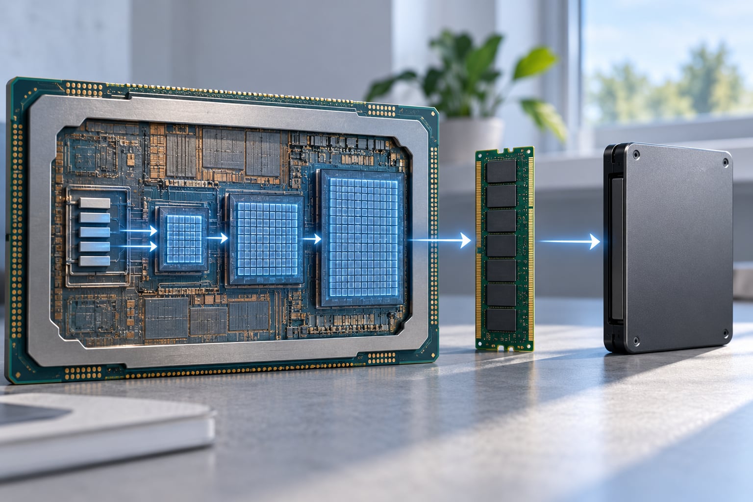
A cache hierarchy is the set of progressively larger but slower memory levels a processor uses to find data fast, running in this order: CPU registers, L1 cache, L2 cache, L3 cache, main memory (DRAM), then secondary storage. Caching works because programs reuse the same data and nearby data, so the small, expensive, on-die SRAM levels absorb most accesses before the slower levels ever see them.
Below is the version I wish someone had handed me when I started reading architecture docs: the levels with real numbers, then the lookup path step by step, then the parts where a designer actually makes trade-offs. Figures are typical ranges, not vendor guarantees, so treat them as order-of-magnitude and check the optimization manual for the part in front of you.
Table of Contents
- What Is a Cache Hierarchy?
- Why Processors Need a Cache Hierarchy
- What Are the Typical Cache Levels?
- Why the SRAM budget is tight on a real die
- How Does a Cache Hit or Miss Happen?
- Why Do CPUs Use Split L1 Caches?
- How Does Cache Locality Improve Performance?
- How locality turns into a hit rate
- What Affects Cache Hit Rate and Miss Cost?
- How Does the Memory Hierarchy Differ by Workload?
- How Do You Analyze Cache Behavior?
- How Can Designers Reduce Cache Misses?
- Software techniques
- Hardware techniques
- Frequently Asked Questions
- Is the cache hierarchy always L1, L2, L3, and RAM?
- Why is L1 cache usually split into instruction and data caches?
- Does a higher cache hit rate always mean better application performance?
- What is the difference between a cache miss and a TLB miss?
- Why can a cache line be larger without always improving performance?
- How should a chip designer choose a cache configuration for a workload?
- Conclusion
What Is a Cache Hierarchy?
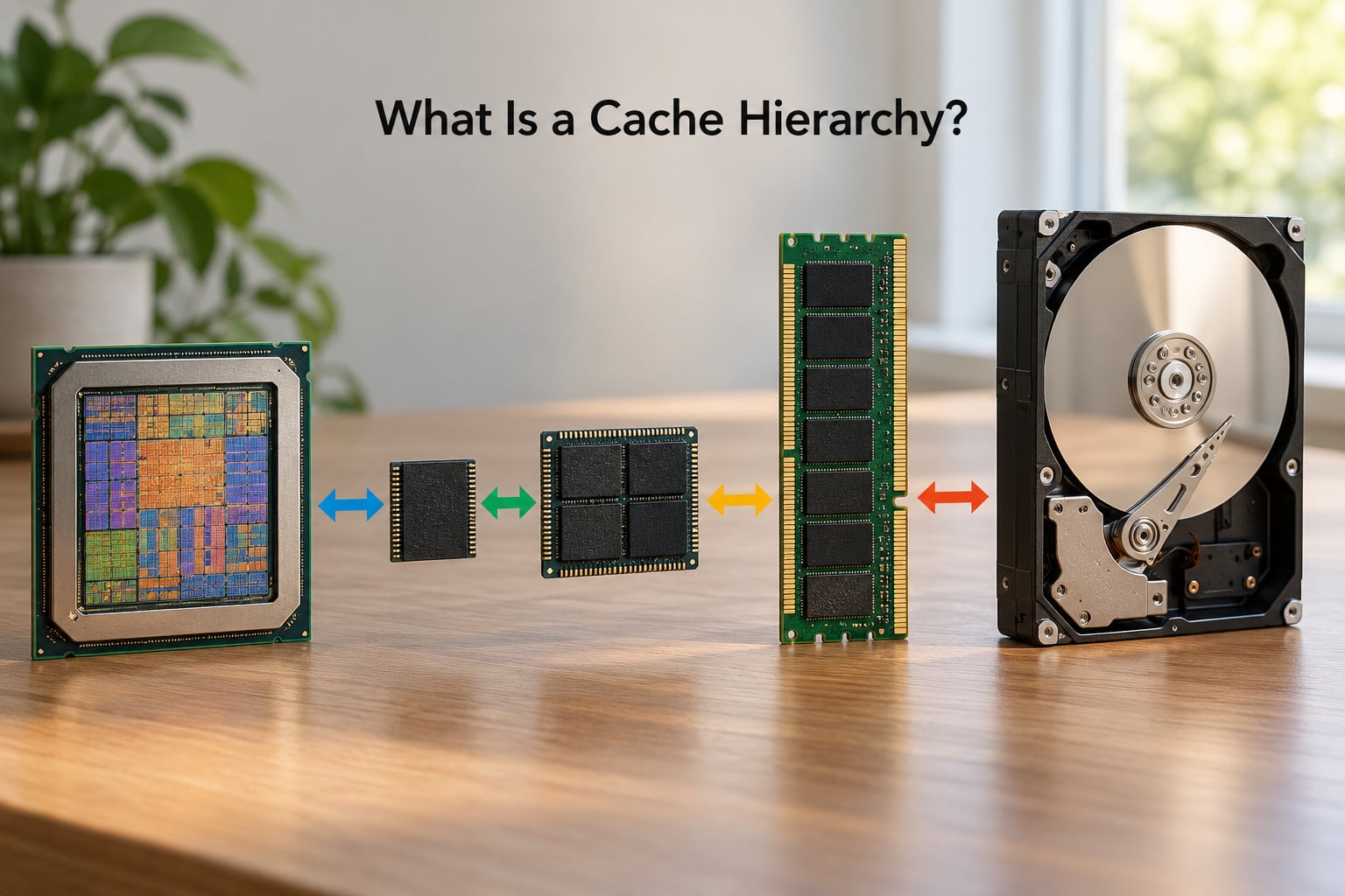
A cache hierarchy is a layered set of memories ordered by speed and capacity. The fastest level is closest to the compute units and the smallest; each level below it is larger, cheaper per bit, and slower to answer. When a lookup misses at one level, the request walks outward until data is found, then copies that data back into the faster levels so the next access hits close to home.
The hierarchy exists because no single memory technology gives you speed and capacity at once. SRAM gives you a few cycles but few bits. DRAM gives you gigabytes but costs hundreds of cycles. Flash and disks give you terabytes at a latency you would never notice if it happened every instruction.
Two numbers describe a level: capacity and access latency. Capacity decides how much of your working set can live there; latency decides what a miss costs you in lost cycles. Everything else in cache design is a way of trading one against the other within a fixed silicon area budget.
Why Processors Need a Cache Hierarchy
The problem is a gap, not a gradient. Logic inside a CPU core has improved far faster per generation than the DRAM attached to it, so the time to fetch one word from main memory has stretched while core throughput has climbed. That divergence is what people call the memory wall.
Without a hierarchy, almost every instruction would stall. A single-cycle load instruction becomes a 200-plus-cycle wait, which means the core spends most of its time idle no matter how many execution units you built. Adding one universal memory type does not fix it: a chip entirely filled with SRAM would either have a tiny capacity or a die so large that yield collapses and power delivery becomes the limiting problem.
Caches break the deadlock by exploiting locality of reference, the statistical fact that a program touches a small region of memory intensively over short windows. Hardware prefetchers also predict sequential and strided streams ahead of the program counter and pull lines in before they are requested.
What Are the Typical Cache Levels?
Five levels cover nearly every design: registers, L1, L2, L3, main memory, then storage as the base. What changes across them is size, technology, scope, and who manages the fill.
| Level | Typical size | Typical latency | Technology | Scope | Managed by |
|---|---|---|---|---|---|
| Registers | Hundreds of bytes per core | About 1 cycle | Flip-flop storage in the core | Per thread, architectural state | Compiler and register renaming |
| L1 cache | 32 to 64 KB per core, split I and D | About 4 to 5 cycles | SRAM | Private per core | Hardware cache controller |
| L2 cache | 512 KB to 2 MB per core | About 12 to 20 cycles | SRAM | Private per core | Hardware cache controller |
| L3 cache | 8 to 64 MB per socket | About 30 to 50 cycles, more across chiplets | SRAM | Shared across cores | Hardware with coherence snooping |
| Main memory | 16 GB to 1 TB+ | About 200 to 400 cycles | DRAM, DDR5 or LPDDR5 | Shared across the socket | Memory controller and OS |
| Secondary storage | 512 GB to many TB | Tens of thousands to millions of cycles | Flash, NVMe or HDD | Per device | Software through a driver and filesystem |
L1 sits closest to the core and splits into an instruction cache and a data cache, which I cover separately below. L2 is large enough to hold a working slice of one thread and typically holds a superset of L1. L3 is the last on-die stop and the most contested capacity, because it competes with core logic and the memory controllers for die area.
Main memory and storage are not caches, but they belong in the same pyramid because the design questions are identical in shape: bigger, cheaper, slower. A designer who reasons only about the cache levels misses the fact that most of a large workload’s time is spent waiting on DRAM after all.
Why the SRAM budget is tight on a real die
On-die SRAM is the most expensive memory per bit on the die. Each bit cell needs roughly six transistors rather than the one transistor plus one capacitor that DRAM uses, and a cache cannot be built from data bits alone: every line carries a valid bit, a dirty bit, and a tag. A nominal 64-byte line occupies on the order of 72 bytes of storage once that metadata is counted, so a cache advertised as 32 MB needs closer to 36 MB of actual array and tag area.
That overhead is why capacity does not scale for free across generations. When a design shrinks its L2 while keeping L3 flat, it is usually trading area for something else, like core count or memory-controller width.
How Does a Cache Hit or Miss Happen?
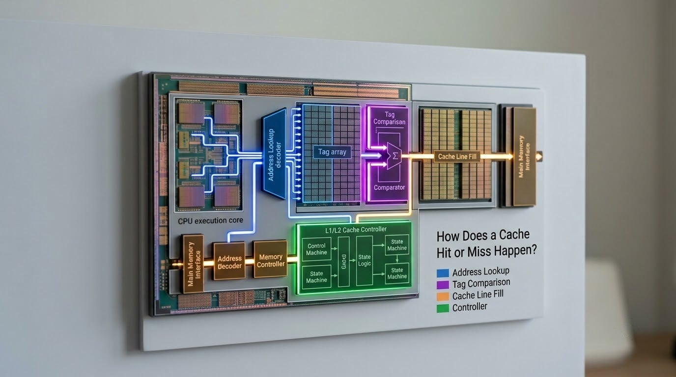
Every load or store address is split into three fields: a tag, a set index, and a block offset. With a 64-byte line, the offset is the low 6 bits. The set index selects which group of lines, or way group, the address can live in. The tag is compared against the tags stored alongside those lines.
The arithmetic is worth doing once by hand. Take a 64 KB, 8-way L1 data cache with 64-byte lines. Capacity divided by line size gives 1024 lines, divided by 8 ways gives 128 sets, so the index is 7 bits. A 32-bit address then splits into a 19-bit tag, a 7-bit index, and a 6-bit offset.
On a read, the index drives the array in parallel across all ways. If any valid line’s tag matches, that is a hit and the offset selects the byte inside the line. If no tag matches, it is a miss, and the controller searches the next level outward.
On a miss, the whole line is fetched, not just the requested word, and it is installed in the victim way. Which way gets evicted depends on the replacement policy: LRU for lightly accessed caches, pseudo-random or RRIP for large shared caches that need to behave predictably under many concurrent streams. Writes depend on the write policy, which is either write-through, sending every update to the next level too, or write-back, marking the line dirty and deferring the update until that line is evicted.
The fill on a miss costs far more than the latency of the next level alone, because it moves the entire line and may stall competing requests. In a small embedded core the difference between a 4-cycle L1 hit and a 30-cycle L2 hit is roughly a factor of seven in how long that one memory operation blocks everything behind it.
Why Do CPUs Use Split L1 Caches?
L1 is split into an instruction cache and a data cache because the two streams behave differently and can be served in parallel. Instruction fetch is a sequential, predictable read pattern; data access is unpredictable in address and involves both reads and writes. Giving each its own array, its own tag store, and its own port lets a load and a fetch complete in the same cycle instead of competing for one structure.
The bandwidth argument matters more than most explanations admit. A single-port unified L1 means one memory operation per cycle, so a core that issues two loads plus a fetch per cycle stalls. Two separate ports roughly double the sustainable request rate for the front end.
There is also an isolation argument. Writes and instruction reads have different hazards. Self-modifying code, where the program rewrites instructions it is about to execute, must either be detected by hardware or handled by explicit cache maintenance, and a split organization makes that detection a local, per-cache problem rather than a coherence question inside one array.
Unified caches do exist, usually at L2 and above where the sharing is worth more than the extra bandwidth. Some cores go further and add a small decoded instruction cache in front of L1i, which stores micro-ops rather than raw bytes and lets the front end skip decode on repeat paths.
How Does Cache Locality Improve Performance?
Locality is the reason the hierarchy gets a high hit rate. Temporal locality means a location accessed recently will be accessed again soon: the top of the stack during a function call, a loop counter, a hot field in a struct. Spatial locality means nearby addresses will be touched soon, which is why fetching a 64-byte line instead of a 4-byte word is almost always the right call.
A loop that walks a row-major array is the clean example. Every access is different, so temporal locality alone would not help, but each access brings the bytes after it into L1 for free, and the next loop iteration re-reads lines that are still resident. Change that same loop to traverse the array column by column and you destroy spatial locality while keeping the same instructions, often running it several times slower on the same silicon.
How locality turns into a hit rate
Average memory access time is the standard summary and it is simple: AMAT equals hit time plus miss rate times miss penalty. Using L1 with a 4-cycle hit time, a 95 percent hit rate, and a 30-cycle miss penalty gives 4 plus 0.05 times 30, which is 5.5 cycles per access. Raise the hit rate to 98 percent and the same formula gives 4.6 cycles, a useful gain for one design change and nothing else.
The formula also shows the limit. Once AMAT approaches the hit time, better L1 hit rates stop buying much, and the next win comes from reducing the penalty or from overlapping misses rather than from shrinking the miss rate further.
Hit rate alone is a weak summary metric. A workload can hit almost everything and still stall if each hit is followed by a dependent load, which is why instructions per cycle and memory-level parallelism matter as much as the counters most beginners watch first.
What Affects Cache Hit Rate and Miss Cost?
Hit rate and miss cost move together. Working-set size versus capacity decides capacity misses. Conflicts between addresses that map to the same set decide conflict misses. Data never touched before decides compulsory misses, and no policy can avoid those beyond a first touch.
Associativity is the hardware lever against conflict misses. A direct-mapped cache has one candidate way per set, so two frequently used addresses with the same index evict each other forever, which is why padding a struct array to avoid power-of-two strides is a real technique. More ways give each address more legal homes and raise the hit rate, at the cost of parallel comparators, more tag storage, and longer lookup in the worst case.
Line size works the same way. A 64-byte line covers spatial locality well and keeps the tag overhead per useful byte low. A 128-byte line fetches more bytes per miss, which helps streaming loops and hurts pointer chasing and small random lookups, because each miss now drags in data nothing will read.
Replacement policy matters most in a large shared cache, where hundreds of streams compete. Pure LRU gives poor behavior under scans because one streaming pass can evict everything, so large caches typically use randomized or RRIP-style policies that age lines in roughly a fixed order and bound how fast a scan can displace hot data.
Finally, latency hiding. Out-of-order cores issue independent loads while earlier ones are outstanding, so several misses can overlap. Hardware prefetchers and explicit prefetch instructions extend that overlap by starting the fetch earlier, and prefetch distance that overruns the cache size turns into pollution that lowers the hit rate for everyone else.
How Does the Memory Hierarchy Differ by Workload?
No workload cares about all levels equally. Sequential streaming saturates bandwidth and cares about DRAM, pointer chasing cares about latency at every level, and tightly coupled instruction and data patterns set the bar for L1 sizing.
| Workload | Locality profile | Dominant bottleneck | What helps most |
|---|---|---|---|
| Sequential streaming, compression, media encode | Strong spatial, weak temporal | DRAM and memory bandwidth | Large line-friendly prefetch, streaming stores that bypass cache |
| Random access, hash table probing | Little spatial, unpredictable | Latency at every level | Higher associativity, deeper out-of-order window, memory-level parallelism |
| Pointer chasing, linked structures | No spatial locality at all | Serial dependent loads | Prefetching hard, software layout, more cores |
| Database-style index lookup | Scattered pages, hot upper levels | TLB misses and DRAM latency | Larger pages, huge pages, hot-set partitioning |
| Tightly coupled compute and memory | Very high spatial and temporal | L1 capacity and port bandwidth | Split L1, enough L1 capacity, register allocation quality |
| Multi-threaded server with shared data | Varies per thread | Coherence traffic and interconnect | Private L2, non-inclusive L3, snoop filtering, careful line padding |
False sharing sits in that last row. Two cores writing different fields of the same cache line invalidate each other’s copy on every write, so throughput collapses even though each thread is only touching its own variable. Padding or aligning hot per-thread counters to a line boundary is the standard fix, and it is a layout change rather than a hardware one.
How Do You Analyze Cache Behavior?
You cannot reason about cache behavior without counters. On Linux, start by reading what the hardware reports, then compare workloads against each other rather than against a theoretical target.
The first command shows every cache level with its size, type, and associativity, and which CPUs share it:
lscpu -CThe sysfs tree gives the same information per level, including the shared CPU list, and is the place to look when you want to confirm that L3 really is shared while L2 is private:
ls /sys/devices/system/cpu/cpu0/cache/
cat /sys/devices/system/cpu/cpu0/cache/index3/level
cat /sys/devices/system/cpu/cpu0/cache/index3/type
cat /sys/devices/system/cpu/cpu0/cache/index3/size
cat /sys/devices/system/cpu/cpu0/cache/index3/shared_cpu_list
For running code, vendor tools expose the useful counters directly: on x86, perf stat -e cache-references,cache-misses,L1-dcache-load-misses gives event counts you can ratio, and perf c2c reports which lines are being ping-ponged between cores, which is how you confirm false sharing instead of guessing. Hardware performance counters still require perf_event_paranoid to permit access, so a restricted container may block the whole approach.
Offline, a cache simulator run against a recorded address trace is the standard design tool. Feed it a trace from a representative workload and you can sweep line size, associativity, and replacement policy without fabricating silicon, which is exactly how a team decides whether a bigger L2 or a smarter policy is the better use of area.
Read the results with care. Compare memory traffic and instructions per cycle before concluding anything from hit rate, because a change that raises the hit rate can still lose overall if it lengthens the critical path.
How Can Designers Reduce Cache Misses?
Both sides of the system have levers, and the ones that matter depend on which miss type is actually occurring. Start from the counters rather than from a favorite technique.
Software techniques
Blocking, or tiling, splits a loop nest into chunks that fit in L1 or L2 so intermediate results stay hot instead of streaming past the cache. Array layout matching the traversal order fixes the column-versus-row case. Padding structures to break power-of-two strides removes conflict misses in direct-mapped and low-associative caches. Loop fusion reduces traffic by keeping a value in a register across iterations that would otherwise reload it.
Two more worth knowing: explicit prefetch instructions let you start a fetch several iterations ahead for known-stride loops, and non-temporal stores write straight past the cache when the data will not be read again soon, which stops streaming operations from evicting useful lines. Non-temporal is the one to use carefully, since it only helps on writes that are truly discarded and are not read soon after.
Hardware techniques
Higher associativity reduces conflict misses at the cost of area and lookup time. A victim cache, a small fully associative structure holding evicted lines, catches a useful slice of capacity and conflict misses cheaply. Cache coloring and address hashing spread physical pages across cache sets and channels to reduce the aliasing that comes from page coloring by the virtual memory system.
Multilevel inclusion policies decide what L3 may hold. An inclusive L3 guarantees any line in L2 is also in L3, which simplifies lookup. An exclusive L3 holds only what no L2 holds, which lowers wasted capacity. Non-inclusive designs need snoop filters or a victim structure so L3 can be searched without every probe broadcasting to every core.
And the physical one that constrains all the others: on-die SRAM area. Adding 8 MB of L3 costs area that would otherwise hold cores or memory-controller width, and that trade is where most cache sizing arguments are really settled.
Frequently Asked Questions
Is the cache hierarchy always L1, L2, L3, and RAM?
No. Registers sit above L1 and storage sits below main memory, so the full picture is registers, L1, L2, L3, RAM, then secondary storage. How many on-die cache levels exist varies by design: some cores have only L1 and a shared last-level cache, some small embedded parts have a single unified cache, and multi-die or chiplet designs can split the last level into a slice per die. The ordering rule is constant even when the count is not.
Why is L1 cache usually split into instruction and data caches?
Instructions and data have different access patterns and different permissions. Instruction fetch is sequential and read-only, while loads and stores are unpredictable and can write. Separate arrays give the core one port for each stream, so a fetch and a load can complete in the same cycle instead of queueing behind one shared structure. The split also keeps data writes from sitting in the same array the front end reads, which simplifies handling of self-modifying code.
Does a higher cache hit rate always mean better application performance?
No. A high hit rate says nothing about how long each access took, how many misses overlapped, or how much memory bandwidth the workload consumed. A kernel with a 99 percent hit rate can still stall if every hit feeds a dependent load with no work to overlap. Look at instructions per cycle, retired stalls on memory operations, and DRAM traffic alongside the hit rate before deciding a design change helped.
What is the difference between a cache miss and a TLB miss?
A cache miss means the data cache does not hold the line for that physical address, so the lookup continues to L2, L3, or main memory. A TLB miss means the translation lookaside buffer does not hold the virtual-to-physical mapping for that virtual address, so the memory management unit has to walk the page table first. A TLB miss therefore usually triggers a cache lookup too, which is why translation cost often shows up inside what looks like a cache stall.
Why can a cache line be larger without always improving performance?
A larger line fetches more bytes per miss, which helps streaming loops but wastes bandwidth on pointer chasing and random lookups where most of the fetched line is never read. It also cuts the number of sets for a fixed capacity, making tags larger and increasing the chance of conflict misses. Larger lines raise effective miss latency too, since transferring twice the data takes longer and a miss blocks the pipeline for the whole fill.
How should a chip designer choose a cache configuration for a workload?
Start from measured behaviour, not intuition. Record an address trace or performance counters from a representative workload, then sweep line size, associativity, and policy in a simulator before committing silicon. Weight the result by where the workload actually stalls: latency-bound code wants associativity and MLP, streaming code wants bandwidth and prefetch, and shared-data code wants private L2 plus a non-inclusive shared level. Finally, check the total SRAM area against core area, since cache capacity competes directly for die.
Conclusion
The cache hierarchy is one idea repeated at different scales: keep what is hot close to the compute, and push the cold stuff somewhere cheap. Registers, L1, L2, L3, DRAM, and storage all obey that rule, differing only in how much capacity they trade away for speed.
When you start reading a design or profiling a workload, do this: identify the locality of the access pattern, then measure hit rate, the source of the misses, and memory traffic for a representative case. Look at which level the stall is actually charged to, and remember that every byte of on-die cache is area taken from something else. That order of thinking is what turns the pyramid diagram into an actual design decision.